OBJECTIVES
• Introduction ofDC-DC Converter
• Voltage Regulation
• Types of DC-DC Converters
• Linear regulator (LR)
• Series regulator
• Shunt regulator.
• Switching mode power supply (SMPS)
• Advantages and Disadvantages
3.
• DC toDC Converters convert DC power to another DC power level or
convert voltage/current to another voltage/current
• Batteries are often shown on a schematic diagram as the source of DC
voltage but usually the actual DC voltage source is a power supply.
• DC to DC converters are important portable electronic devices used
whenever we want to change DC electrical power efficiently from one
voltage level to another.
• A power converter generates output voltage and current for the load from
a given input power source.
• Depending on the specific application, either a linear regulator (LR) or a
switching mode power supply (SMPS) solution to be chosen.
Introduction
4.
• Car battery12V must be stepped down to 3-5V DC voltage to run DVD/CD player
• Laptop computers or cellular phone battery voltage must be stepped down to
run several sub-circuts, each with its own voltage level requirement different
from that supplied by the battery.
• Single cell 1.5 V DC must be stepped up to 5V operate an electronic circuitry.
• A 6V or 9V DC must be stepped up to 500V DC or more, to provide an insulation
testing voltage.
• A 12V DC must be stepped up to +/-40V or so, to run a car hifi amplifier circuitry.
• A 12V DC must be stepped up to 650V DC or so, as part of a DC-AC sinewave
inverter.
Typical Application of DC-DC converter
5.
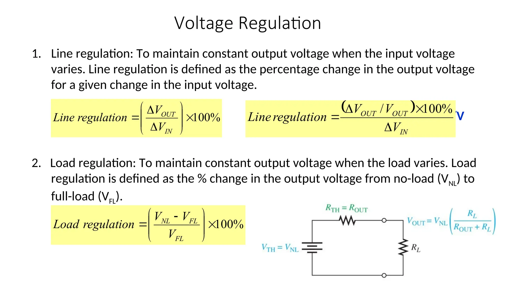
Voltage Regulation
1. Lineregulation: To maintain constant output voltage when the input voltage
varies. Line regulation is defined as the percentage change in the output voltage
for a given change in the input voltage.
or %/V
2. Load regulation: To maintain constant output voltage when the load varies. Load
regulation is defined as the % change in the output voltage from no-load (VNL) to
full-load (VFL).
%
100
FL
FL
NL
V
V
V
regulation
Load
%
100
IN
OUT
V
V
regulation
Line
IN
OUT
OUT
V
V
V
regulation
Line
%
100
/
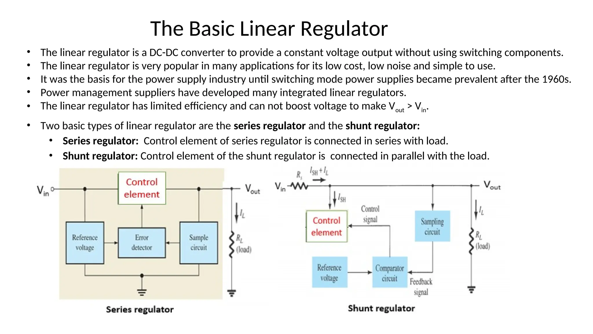
• The linearregulator is a DC-DC converter to provide a constant voltage output without using switching components.
• The linear regulator is very popular in many applications for its low cost, low noise and simple to use.
• It was the basis for the power supply industry until switching mode power supplies became prevalent after the 1960s.
• Power management suppliers have developed many integrated linear regulators.
• The linear regulator has limited efficiency and can not boost voltage to make Vout > Vin.
• Two basic types of linear regulator are the series regulator and the shunt regulator:
• Series regulator: Control element of series regulator is connected in series with load.
• Shunt regulator: Control element of the shunt regulator is connected in parallel with the load.
The Basic Linear Regulator
8.
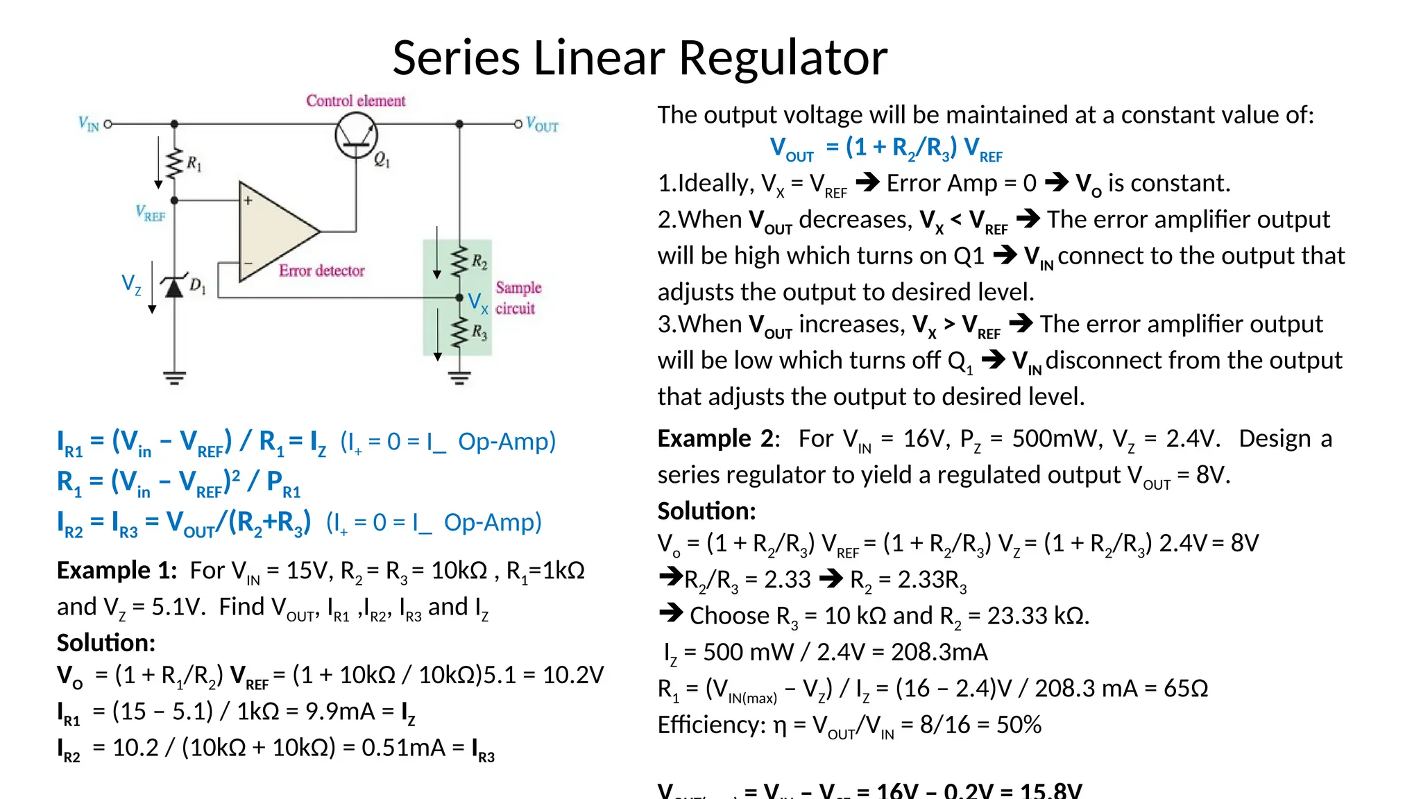
The output voltagewill be maintained at a constant value of:
VOUT = (1 + R2/R3) VREF
1.Ideally, VX = VREF Error Amp = 0 VO is constant.
2.When VOUT decreases, VX < VREF The error amplifier output
will be high which turns on Q1 VIN connect to the output that
adjusts the output to desired level.
3.When VOUT increases, VX > VREF The error amplifier output
will be low which turns off Q1 VIN disconnect from the output
that adjusts the output to desired level.
Series Linear Regulator
Example 1: For VIN = 15V, R2 = R3 = 10kΩ , R1=1kΩ
and VZ = 5.1V. Find VOUT, IR1 ,IR2, IR3 and IZ
Solution:
VO = (1 + R1/R2) VREF = (1 + 10kΩ / 10kΩ)5.1 = 10.2V
IR1 = (15 – 5.1) / 1kΩ = 9.9mA = IZ
IR2 = 10.2 / (10kΩ + 10kΩ) = 0.51mA = IR3
IR1 = (Vin – VREF) / R1 = IZ (I+ = 0 = I_ Op-Amp)
R1 = (Vin – VREF)2
/ PR1
IR2 = IR3 = VOUT/(R2+R3) (I+ = 0 = I_ Op-Amp)
Example 2: For VIN = 16V, PZ = 500mW, VZ = 2.4V. Design a
series regulator to yield a regulated output VOUT = 8V.
Solution:
Vo = (1 + R2/R3) VREF = (1 + R2/R3) VZ = (1 + R2/R3) 2.4V= 8V
R2/R3 = 2.33 R2 = 2.33R3
Choose R3 = 10 kΩ and R2 = 23.33 kΩ.
IZ = 500 mW / 2.4V = 208.3mA
R1 = (VIN(max) – VZ) / IZ = (16 – 2.4)V / 208.3 mA = 65Ω
Efficiency: η = VOUT/VIN = 8/16 = 50%
VX
VZ
9.
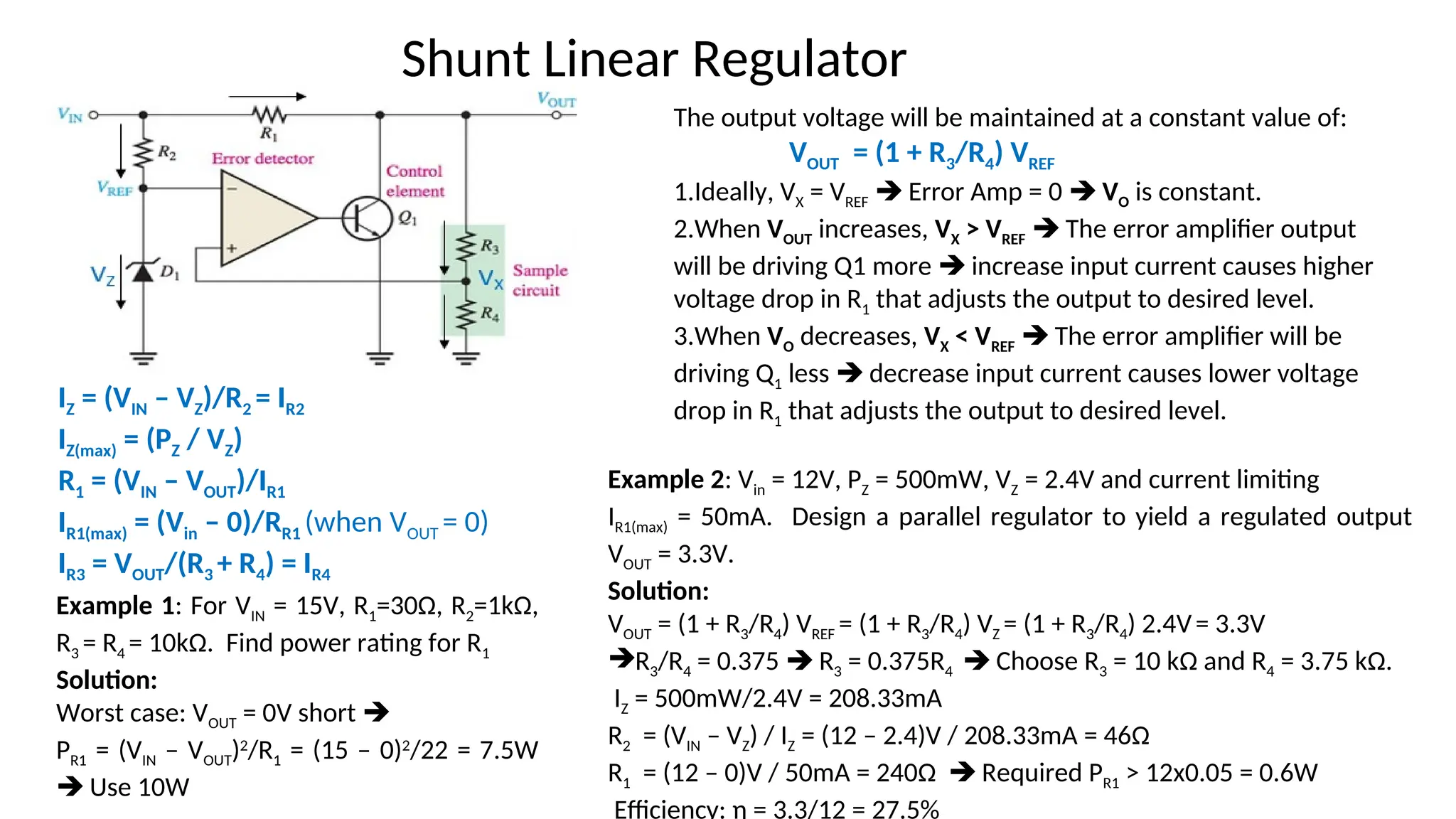
The output voltagewill be maintained at a constant value of:
VOUT = (1 + R3/R4) VREF
1.Ideally, VX = VREF Error Amp = 0 VO is constant.
2.When VOUT increases, VX > VREF The error amplifier output
will be driving Q1 more increase input current causes higher
voltage drop in R1 that adjusts the output to desired level.
3.When VO decreases, VX < VREF The error amplifier will be
driving Q1 less decrease input current causes lower voltage
drop in R1 that adjusts the output to desired level.
Shunt Linear Regulator
IZ = (VIN – VZ)/R2 = IR2
IZ(max) = (PZ / VZ)
R1 = (VIN – VOUT)/IR1
IR1(max) = (Vin – 0)/RR1 (when VOUT = 0)
IR3 = VOUT/(R3 + R4) = IR4
Example 1: For VIN = 15V, R1=30Ω, R2=1kΩ,
R3 = R4 = 10kΩ. Find power rating for R1
Solution:
Worst case: VOUT = 0V short
PR1 = (VIN – VOUT)2
/R1 = (15 – 0)2
/22 = 7.5W
Use 10W
Example 2: Vin = 12V, PZ = 500mW, VZ = 2.4V and current limiting
IR1(max) = 50mA. Design a parallel regulator to yield a regulated output
VOUT = 3.3V.
Solution:
VOUT = (1 + R3/R4) VREF = (1 + R3/R4) VZ = (1 + R3/R4) 2.4V= 3.3V
R3/R4 = 0.375 R3 = 0.375R4 Choose R3 = 10 kΩ and R4 = 3.75 kΩ.
IZ = 500mW/2.4V = 208.33mA
R2 = (VIN – VZ) / IZ = (12 – 2.4)V / 208.33mA = 46Ω
R1 = (12 – 0)V / 50mA = 240Ω Required PR1 > 12x0.05 = 0.6W
Efficiency: η = 3.3/12 = 27.5%
10.
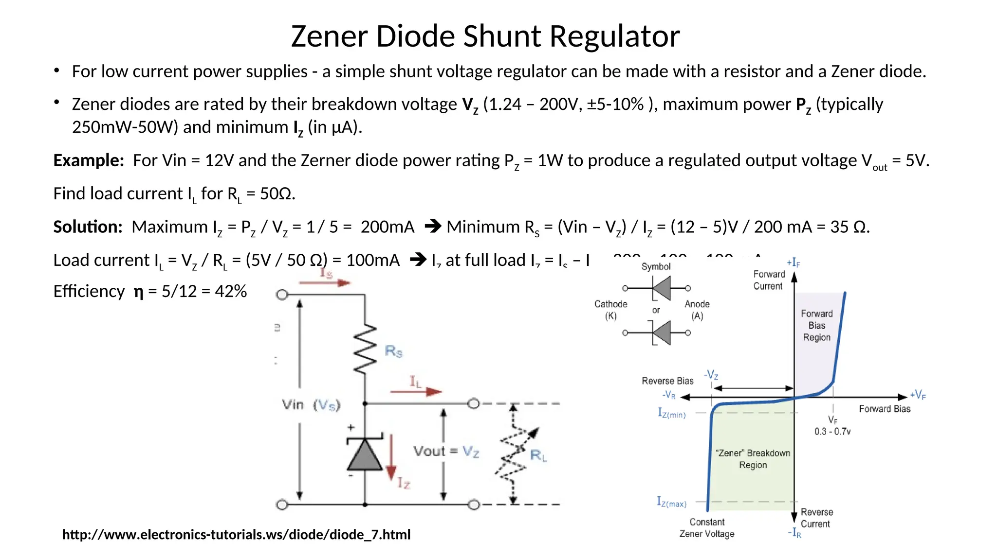
• For lowcurrent power supplies - a simple shunt voltage regulator can be made with a resistor and a Zener diode.
• Zener diodes are rated by their breakdown voltage VZ (1.24 – 200V, ±5-10% ), maximum power PZ (typically
250mW-50W) and minimum IZ (in µA).
Example: For Vin = 12V and the Zerner diode power rating PZ = 1W to produce a regulated output voltage Vout = 5V.
Find load current IL for RL = 50Ω.
Solution: Maximum IZ = PZ / VZ = 1/ 5 = 200mA Minimum RS = (Vin – VZ) / IZ = (12 – 5)V / 200 mA = 35 Ω.
Load current IL = VZ / RL = (5V / 50 Ω) = 100mA IZ at full load IZ = IS – IL = 200 – 100 = 100 mA
Efficiency η = 5/12 = 42%
Zener Diode Shunt Regulator
http://www.electronics-tutorials.ws/diode/diode_7.html
11.
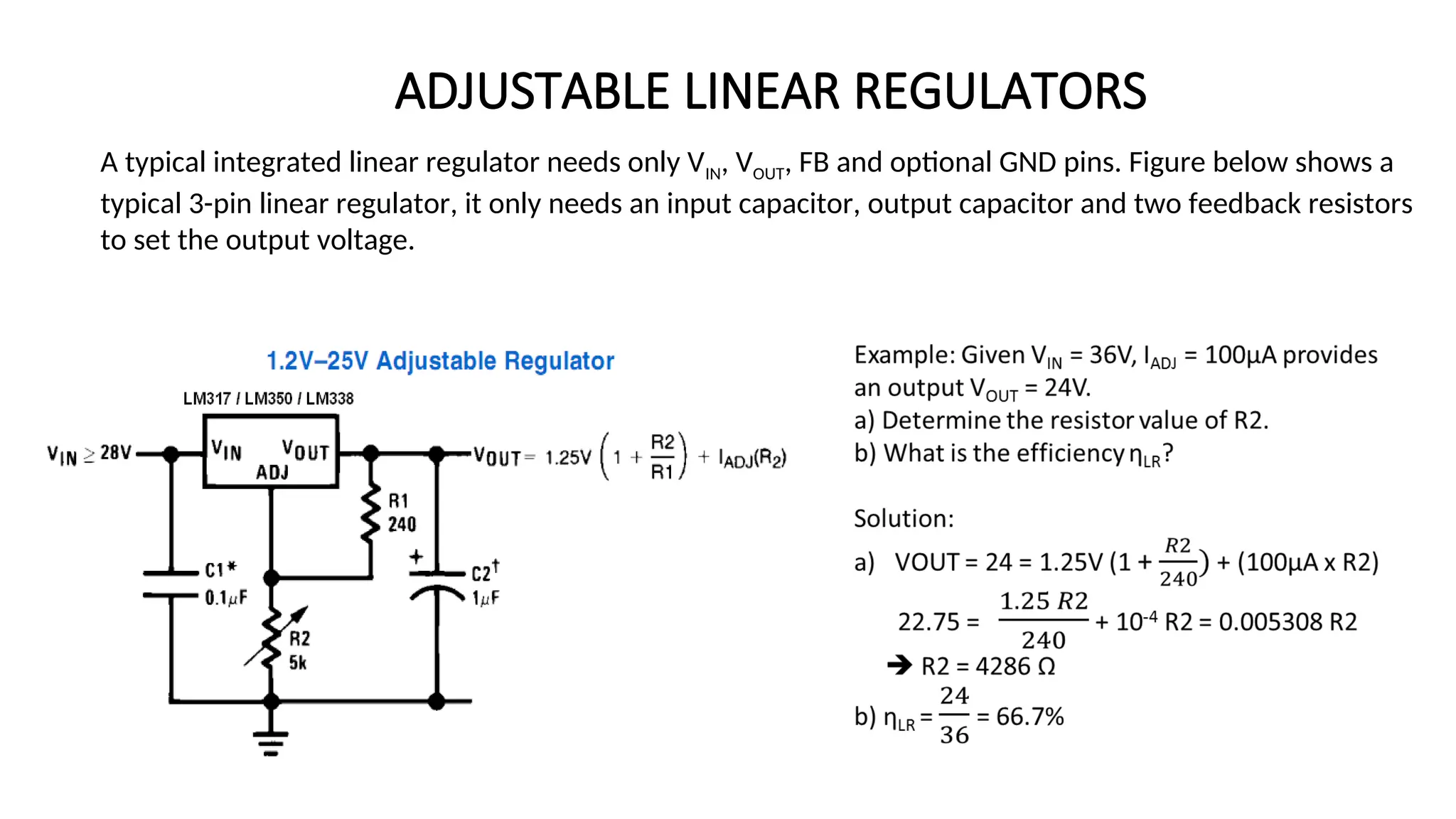
A typical integratedlinear regulator needs only VIN, VOUT, FB and optional GND pins. Figure below shows a
typical 3-pin linear regulator, it only needs an input capacitor, output capacitor and two feedback resistors
to set the output voltage.
ADJUSTABLE LINEAR REGULATORS
12.
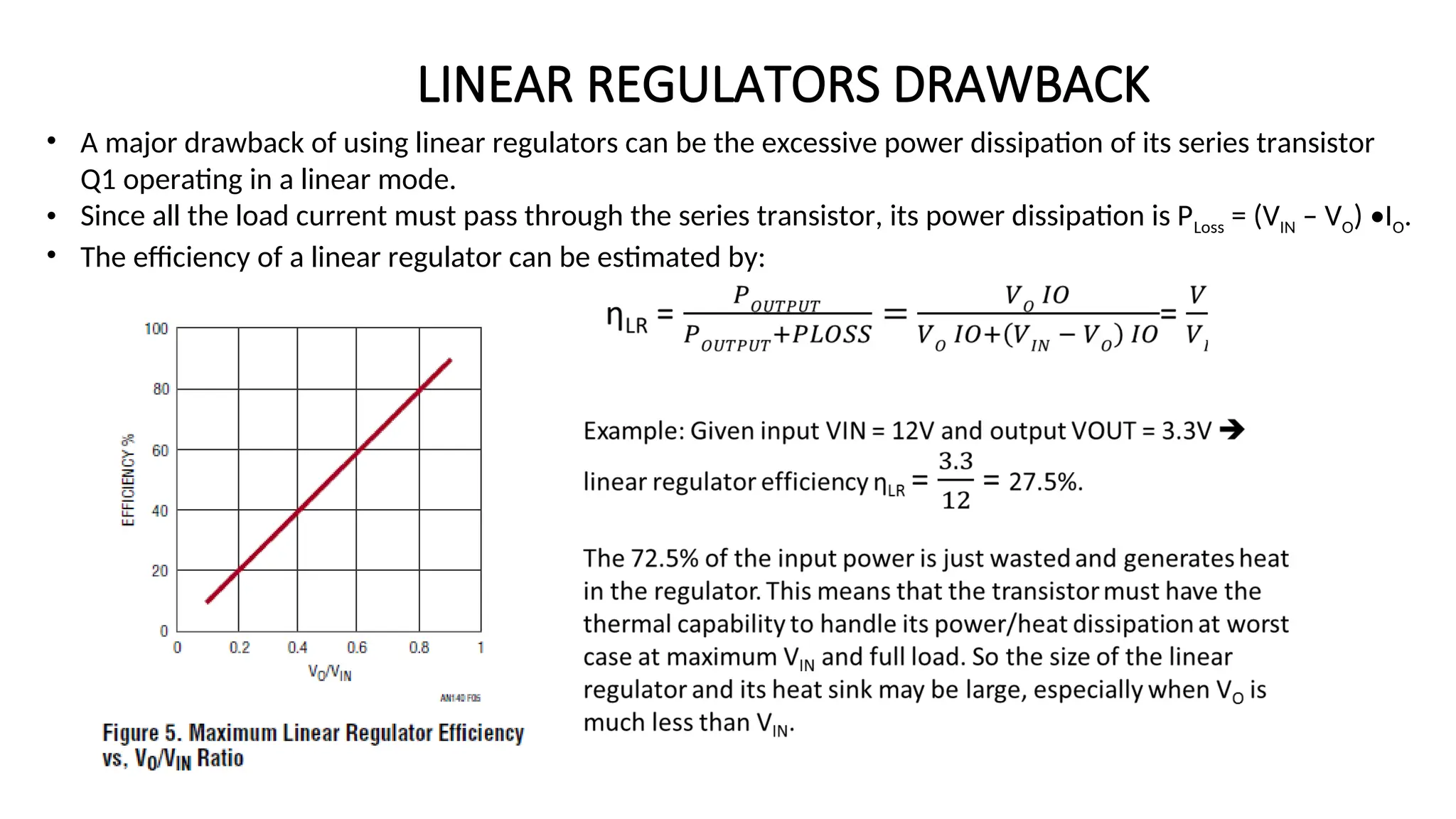
LINEAR REGULATORS DRAWBACK
•A major drawback of using linear regulators can be the excessive power dissipation of its series transistor
Q1 operating in a linear mode.
• Since all the load current must pass through the series transistor, its power dissipation is PLoss = (VIN – VO) •IO.
• The efficiency of a linear regulator can be estimated by:
13.
₊ Low numberof components makes linear power supplies very cost-effectiveness overall and space
savings (unless heat sink is used).
₊ Simplicity and low complexity design makes linear power supplies more reliable.
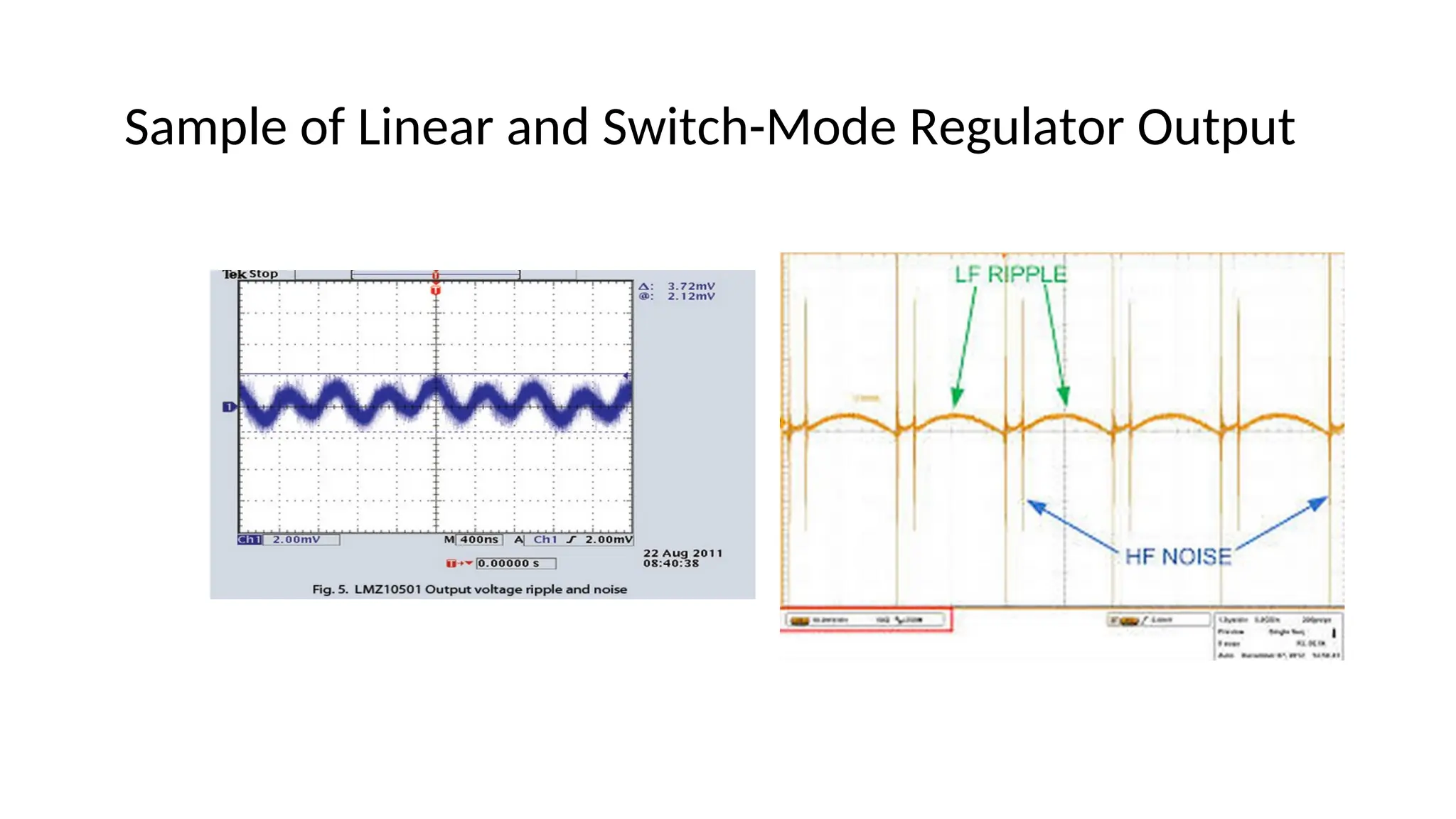
₊ No switching noise and low output voltage ripple makes linear power supplies best suitable for
applications where noise-sensitivity is essential.
₊ Low output voltage ripple
₊ The linear regulator is free of any switching noise, having ripple rejection capability and its low voltage
noise, which makes the linear regulator of choice in such noise-averse applications as audio-visual,
communication, medical, and measurement devices.
Linear Regulators Advantages
14.
• The linearregulator can be very efficient only if VO is close to VIN.
• The linear regulator (LR) has another limitation, which is the minimum voltage difference between VIN and VO. The
transistor in the LR must be operated in its linear mode. So it requires a certain minimum voltage drop across the
collector to emitter of a bipolar transistor or drain to source of a FET. When VO is too close to VIN, the LR may be
unable to regulate output voltage anymore.
• The linear regulators that can work with low headroom (VIN – VO) are called low dropout regulators (LDOs).
• The linear regulator or an LDO can only provide step-down DC/DC conversion.
• Typical design may require a heat sink.
• These disadvantages to linear power supplies include size, high heat loss, and lower efficiency levels when
compared to a switch-mode power supply. The problem with linear power supply units, when used in a high
power application, is that it requires a large transformer and other large components to handle the power. Using
larger components increases the overall size and weight of the power supply and can pose a challenge for weight
distribution within a given application.
Linear Regulators Disadvantages
15.
LINEAR REGULATORS APPLICATIONS
Thereare many applications in which linear regulators provide superior solutions to switching supplies:
1. Simple/low cost solutions. Linear regulator or LDO solutions are simple and easy to use, especially
for low power applications with low output current where thermal stress is not critical. No external
power inductor is required.
2. Low noise/low ripple applications. For noise-sensitive applications, such as communication and radio
devices, minimizing the supply noise is very critical.
3. Fast transient applications. The linear regulator feedback
loop is usually internal, so no external compensation
is required.
4. Low dropout applications. For applications where output voltage is close to the input voltage, LDOs
may be more efficient than an SMPS.
We see that price sensitive applications prefer linear regulators over their sampled-time counterparts.
The design decision is especially clear cut for makers of:
• communications equipment
• small devices
• battery operated systems
• low current devices
• high performance microprocessors with sleep mode (fast transient recovery required)
16.
Regulators Linear regulatorsare less energy efficient than switching regulators. Why do we
continue using them?
Depending upon the application, linear regulators have several redeeming features:
• lower output noise is important for radios and other communications equipment
• faster response to input and output transients
• easier to use because they require only filter capacitors for operation
• generally smaller in size (no magnetics required)
• less expensive (simpler internal circuitry and no magnetics required)
Furthermore, in applications using low input-to-output voltage differentials, the efficiency is not
all that bad! For example, in a 5V to 3.3V microprocessor application, linear regulator efficiency
approaches 66%. And applications with low current subcircuits may not care that regulator
efficiency is less than optimum as the power lost may be negligible overall.
LINEAR REGULATORS VS SWITCHING
REGULATORS
17.
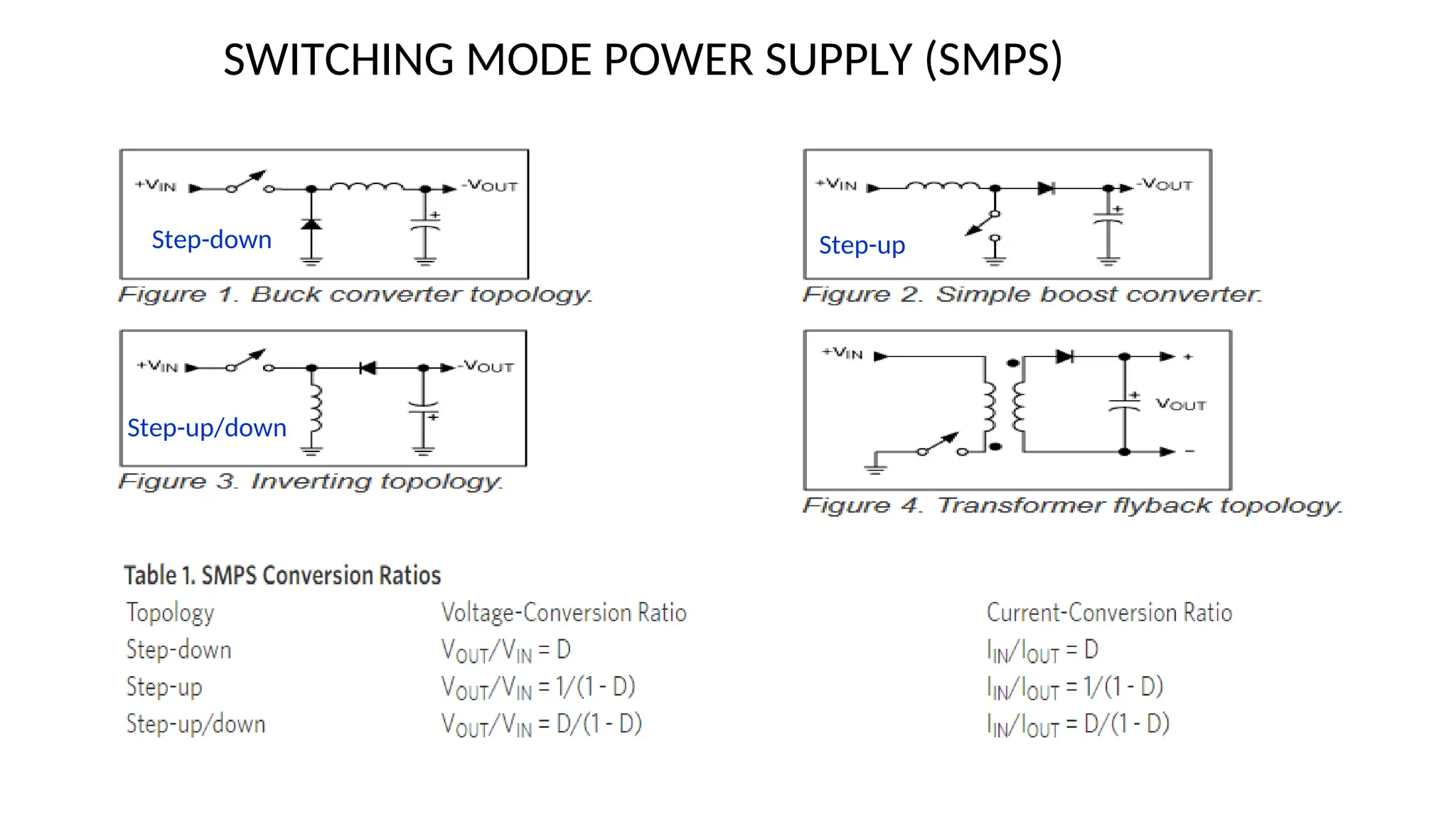
• The switching-modepower supply is a power supply that provides the power supply function through low loss
components such as capacitors, inductors, and transformers -- and the use of switches that are in one of two states,
on or off.
• It offers high power conversion efficiency and design flexibility.
• It can step down or step up output voltage.
• The term switchmode was widely used for this type of power supply until Motorola, Inc., who used the trademark
SWITCHMODE TM
for products aimed at the switching-mode power supply market, started to enforce their
trademark. Switching-mode power supply or switching power supply are used to avoid infringing on the trademark.
• Typical switching frequencies lie in the range 1 kHz to 1 MHz, depending on the speed of the semiconductor
devices.
• Types of SMPS:
• Buck converter: Voltage to voltage converter, step down.
• Boost Converter: Voltage to voltage converter, step up.
• Buck-Boost or FlyBack Converter: Voltage-Voltage, step up and down (negative voltages)
• Cuk Converter: Current-Current converter, step up and down
These converters typically have a full wave rectifier front-end to produce a high DC voltages
SWITCHING MODE POWER SUPPLY (SMPS)
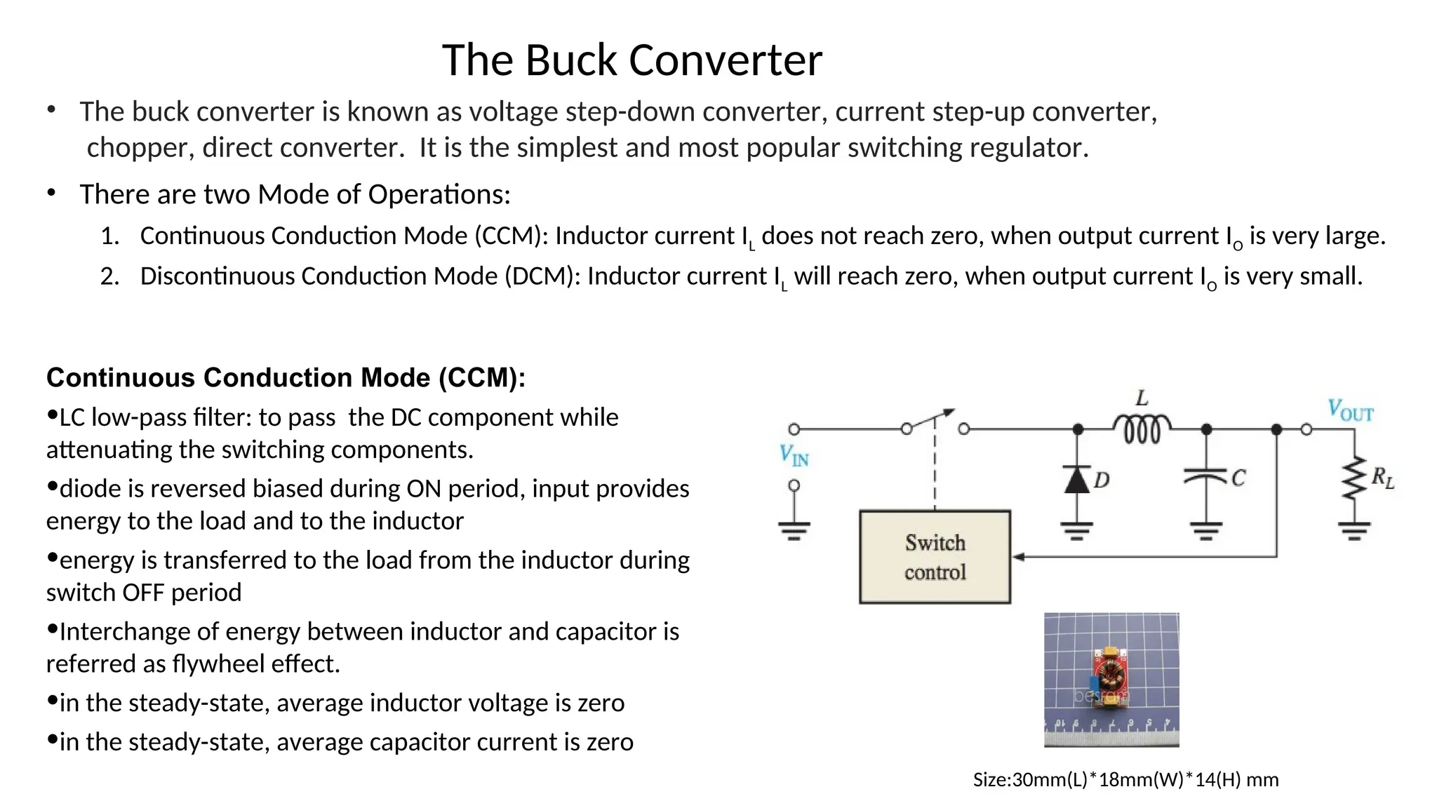
• The buckconverter is known as voltage step-down converter, current step-up converter,
chopper, direct converter. It is the simplest and most popular switching regulator.
• There are two Mode of Operations:
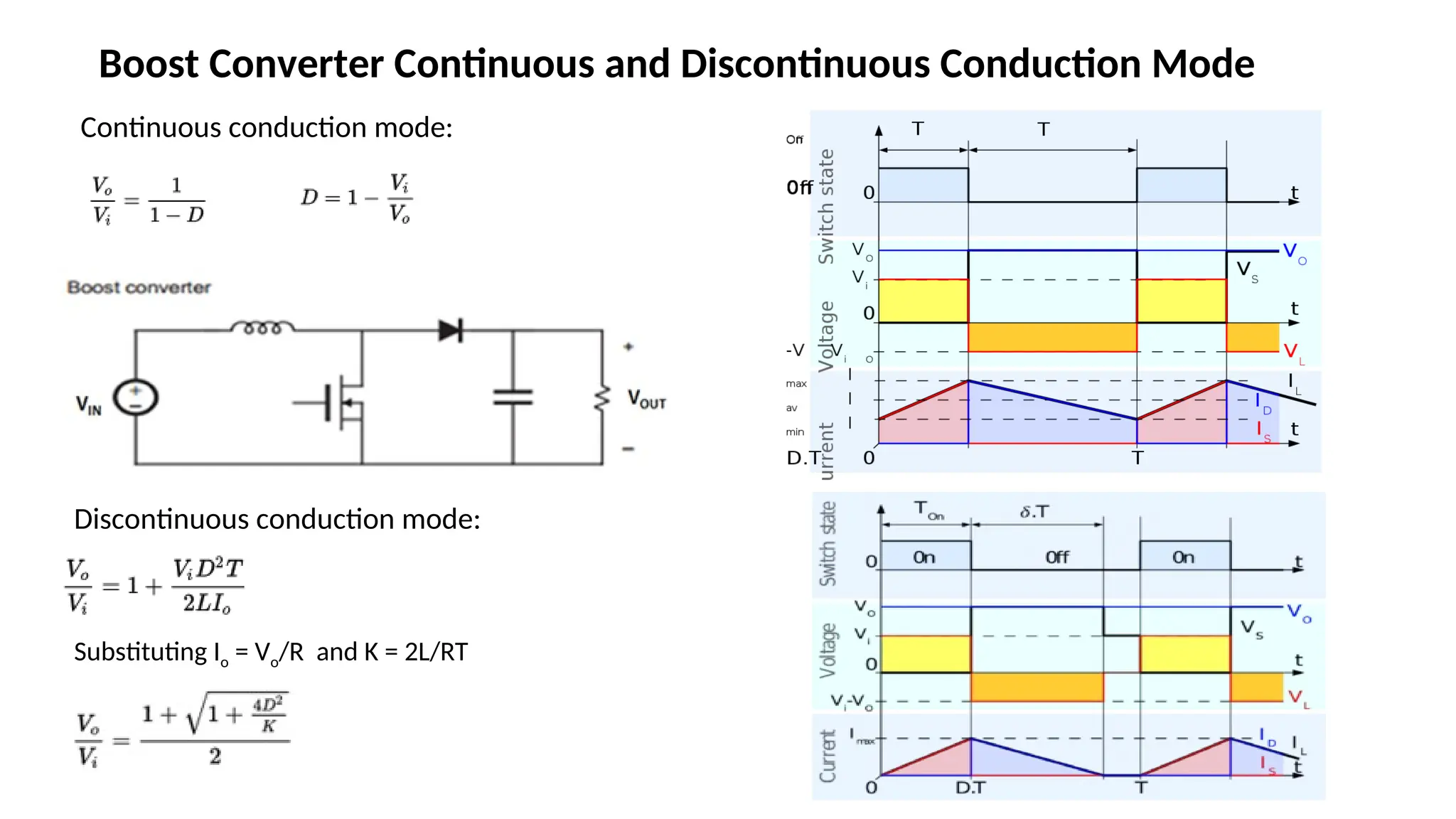
1. Continuous Conduction Mode (CCM): Inductor current IL does not reach zero, when output current IO is very large.
2. Discontinuous Conduction Mode (DCM): Inductor current IL will reach zero, when output current IO is very small.
Size:30mm(L)*18mm(W)*14(H) mm
The Buck Converter
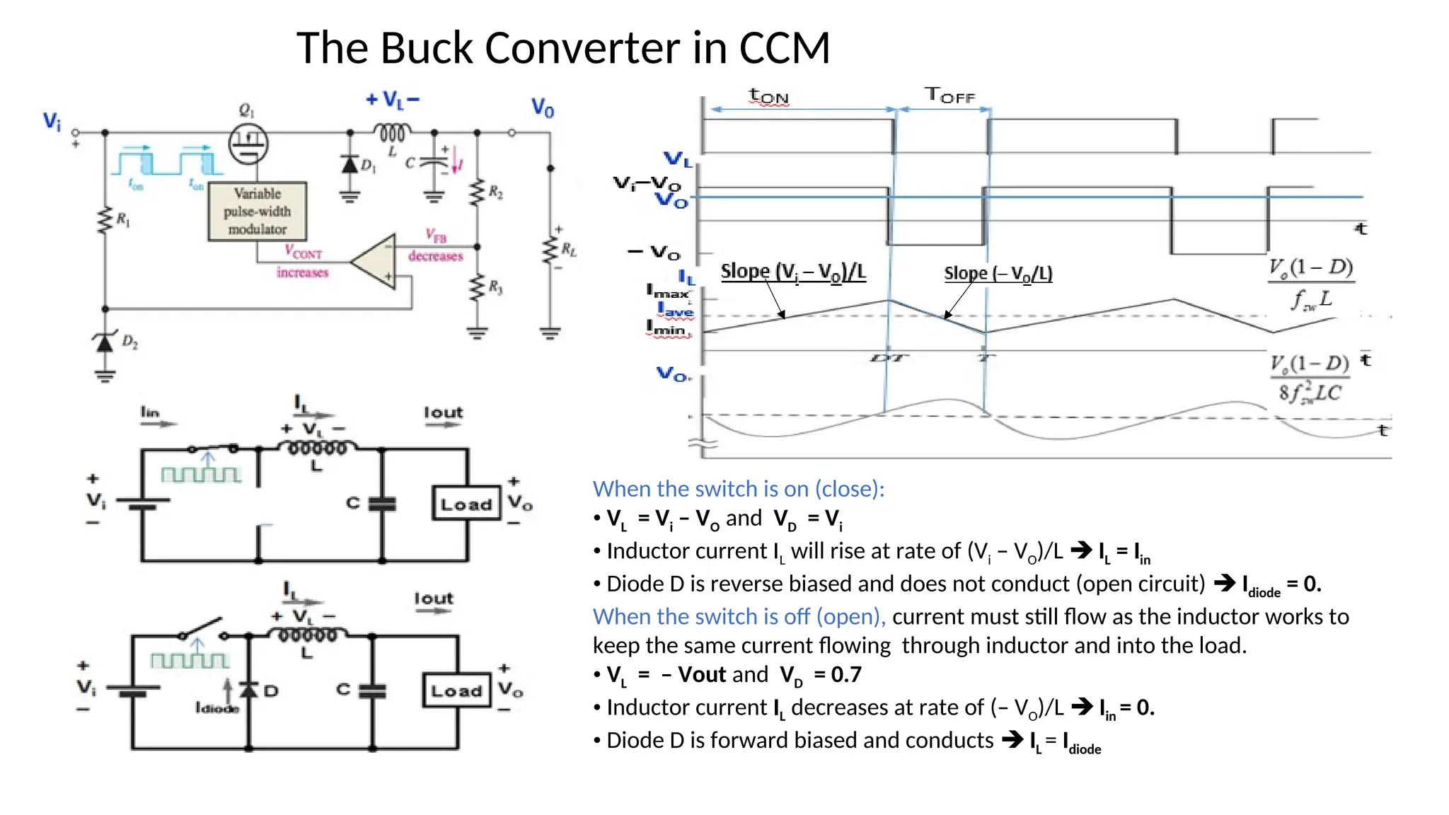
Continuous Conduction Mode (CCM):
•LC low-pass filter: to pass the DC component while
attenuating the switching components.
•diode is reversed biased during ON period, input provides
energy to the load and to the inductor
•energy is transferred to the load from the inductor during
switch OFF period
•Interchange of energy between inductor and capacitor is
referred as flywheel effect.
•in the steady-state, average inductor voltage is zero
•in the steady-state, average capacitor current is zero
21.
When the switchis on (close):
• VL = Vi – VO and VD = Vi
• Inductor current IL will rise at rate of (Vi – VO)/L IL = Iin
• Diode D is reverse biased and does not conduct (open circuit) Idiode = 0.
When the switch is off (open), current must still flow as the inductor works to
keep the same current flowing through inductor and into the load.
• VL = – Vout and VD = 0.7
• Inductor current IL decreases at rate of (– VO)/L Iin = 0.
• Diode D is forward biased and conducts IL = Idiode
The Buck Converter in CCM
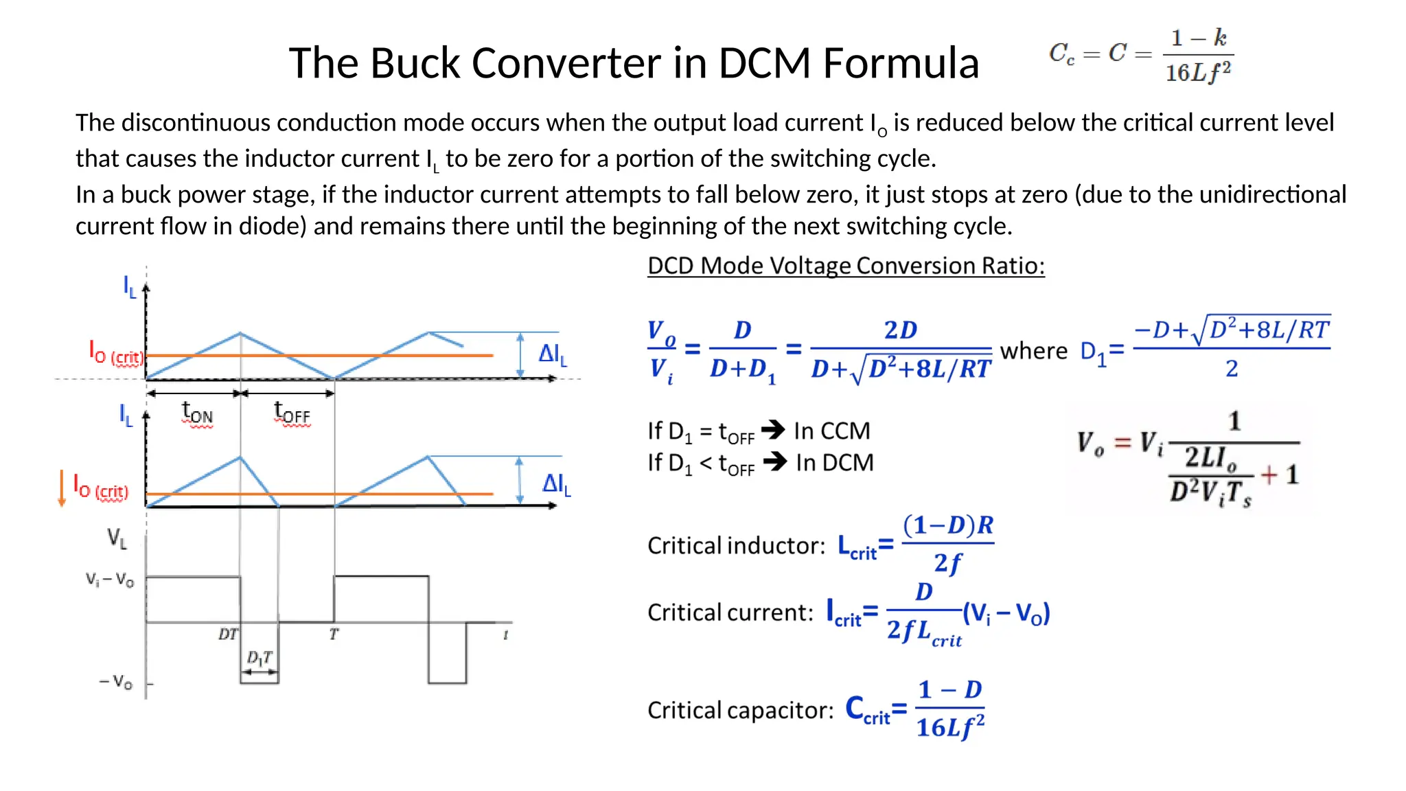
The Buck Converterin DCM Formula
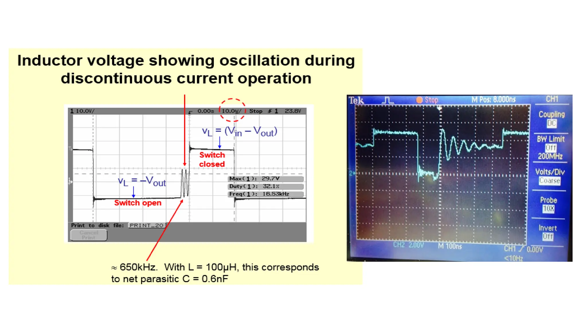
The discontinuous conduction mode occurs when the output load current IO is reduced below the critical current level
that causes the inductor current IL to be zero for a portion of the switching cycle.
In a buck power stage, if the inductor current attempts to fall below zero, it just stops at zero (due to the unidirectional
current flow in diode) and remains there until the beginning of the next switching cycle.
25.
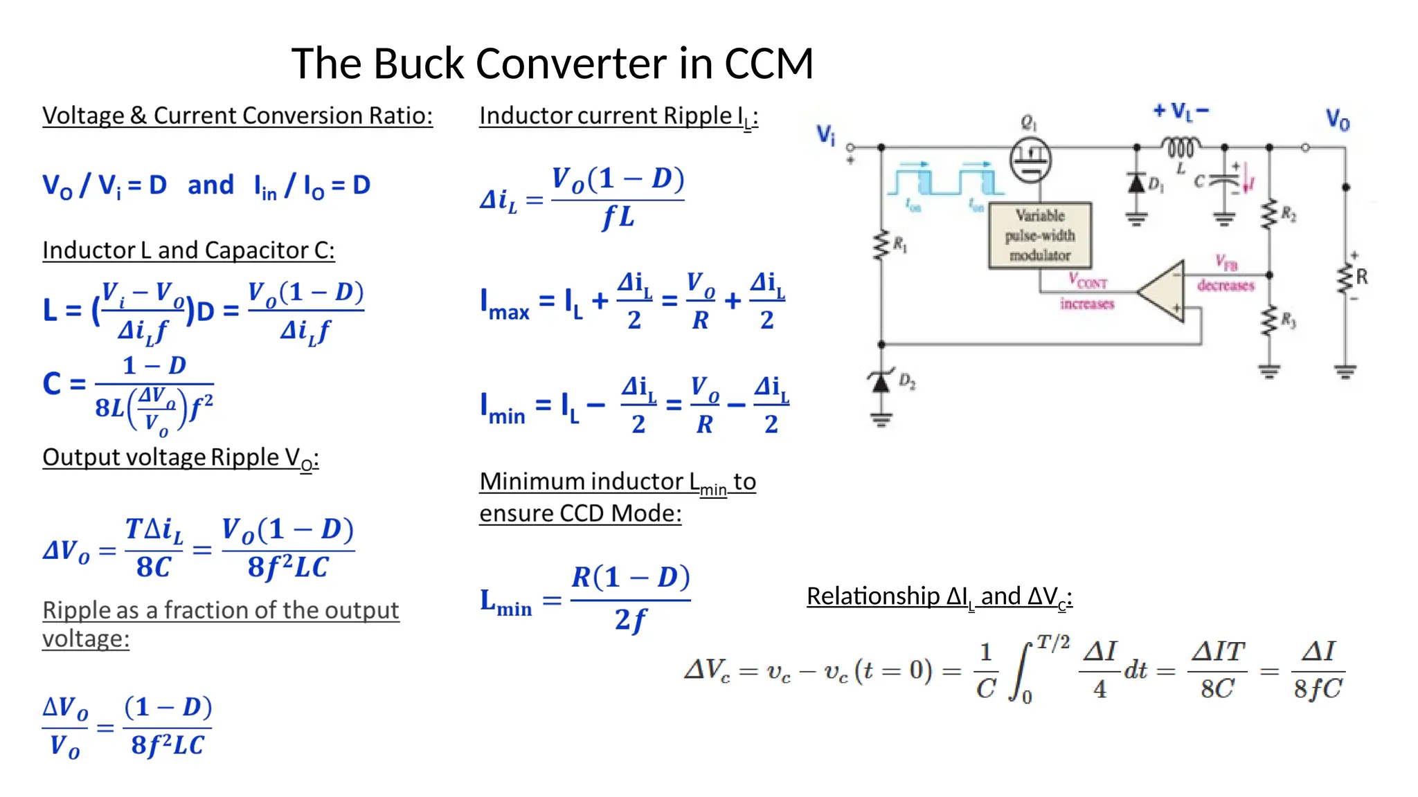
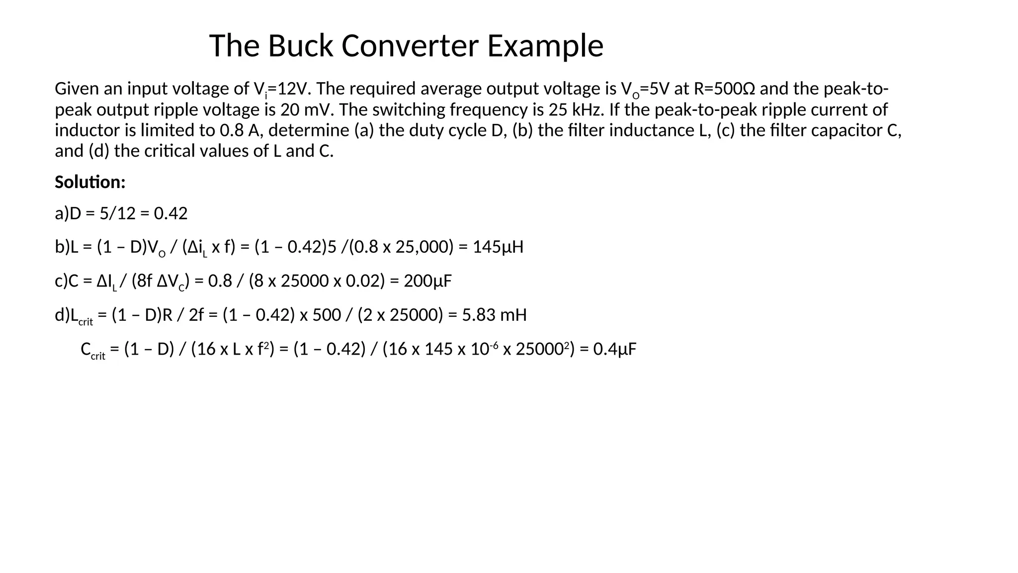
Given an inputvoltage of Vi=12V. The required average output voltage is VO=5V at R=500Ω and the peak-to-
peak output ripple voltage is 20 mV. The switching frequency is 25 kHz. If the peak-to-peak ripple current of
inductor is limited to 0.8 A, determine (a) the duty cycle D, (b) the filter inductance L, (c) the filter capacitor C,
and (d) the critical values of L and C.
Solution:
a)D = 5/12 = 0.42
b)L = (1 – D)VO / (ΔiL x f) = (1 – 0.42)5 /(0.8 x 25,000) = 145μH
c)C = ΔIL / (8f ΔVC) = 0.8 / (8 x 25000 x 0.02) = 200μF
d)Lcrit = (1 – D)R / 2f = (1 – 0.42) x 500 / (2 x 25000) = 5.83 mH
Ccrit = (1 – D) / (16 x L x f2
) = (1 – 0.42) / (16 x 145 x 10-6
x 250002
) = 0.4μF
The Buck Converter Example
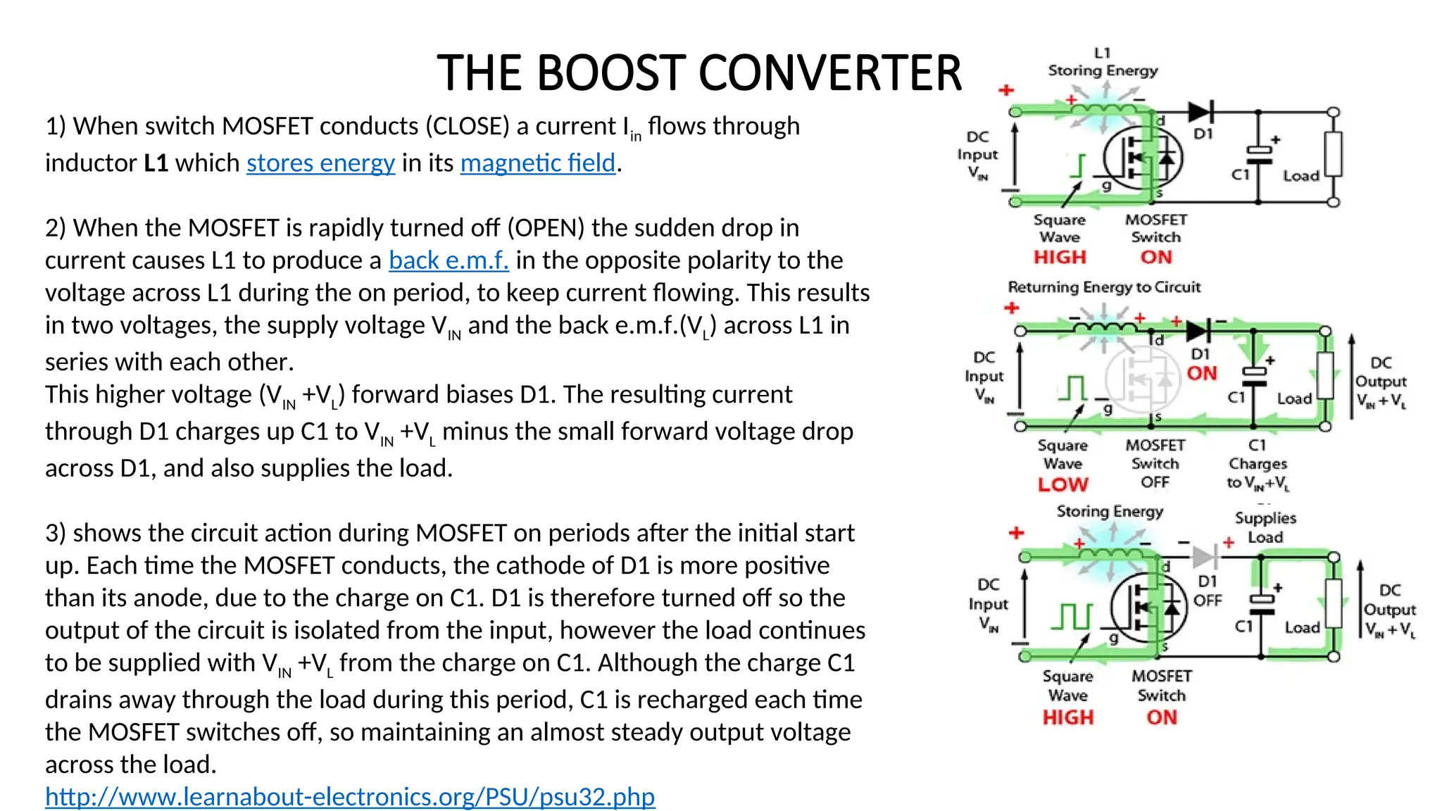
1) When switchMOSFET conducts (CLOSE) a current Iin flows through
inductor L1 which stores energy in its magnetic field.
2) When the MOSFET is rapidly turned off (OPEN) the sudden drop in
current causes L1 to produce a back e.m.f. in the opposite polarity to the
voltage across L1 during the on period, to keep current flowing. This results
in two voltages, the supply voltage VIN and the back e.m.f.(VL) across L1 in
series with each other.
This higher voltage (VIN +VL) forward biases D1. The resulting current
through D1 charges up C1 to VIN +VL minus the small forward voltage drop
across D1, and also supplies the load.
3) shows the circuit action during MOSFET on periods after the initial start
up. Each time the MOSFET conducts, the cathode of D1 is more positive
than its anode, due to the charge on C1. D1 is therefore turned off so the
output of the circuit is isolated from the input, however the load continues
to be supplied with VIN +VL from the charge on C1. Although the charge C1
drains away through the load during this period, C1 is recharged each time
the MOSFET switches off, so maintaining an almost steady output voltage
across the load.
http://www.learnabout-electronics.org/PSU/psu32.php
THE BOOST CONVERTER
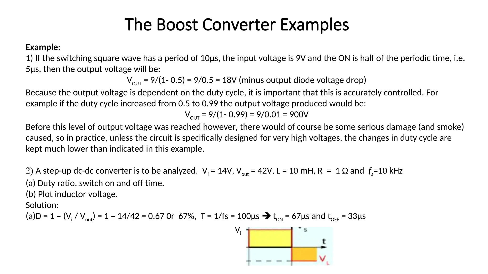
Example:
1) If theswitching square wave has a period of 10µs, the input voltage is 9V and the ON is half of the periodic time, i.e.
5µs, then the output voltage will be:
VOUT = 9/(1- 0.5) = 9/0.5 = 18V (minus output diode voltage drop)
Because the output voltage is dependent on the duty cycle, it is important that this is accurately controlled. For
example if the duty cycle increased from 0.5 to 0.99 the output voltage produced would be:
VOUT = 9/(1- 0.99) = 9/0.01 = 900V
Before this level of output voltage was reached however, there would of course be some serious damage (and smoke)
caused, so in practice, unless the circuit is specifically designed for very high voltages, the changes in duty cycle are
kept much lower than indicated in this example.
2) A step-up dc-dc converter is to be analyzed. Vi = 14V, Vout = 42V, L = 10 mH, R = 1 Ω and fs=10 kHz
(a) Duty ratio, switch on and off time.
(b) Plot inductor voltage.
Solution:
(a)D = 1 – (Vi / Vout) = 1 – 14/42 = 0.67 0r 67%, T = 1/fs = 100µs tON = 67µs and tOFF = 33µs
The Boost Converter Examples
Vi
31.
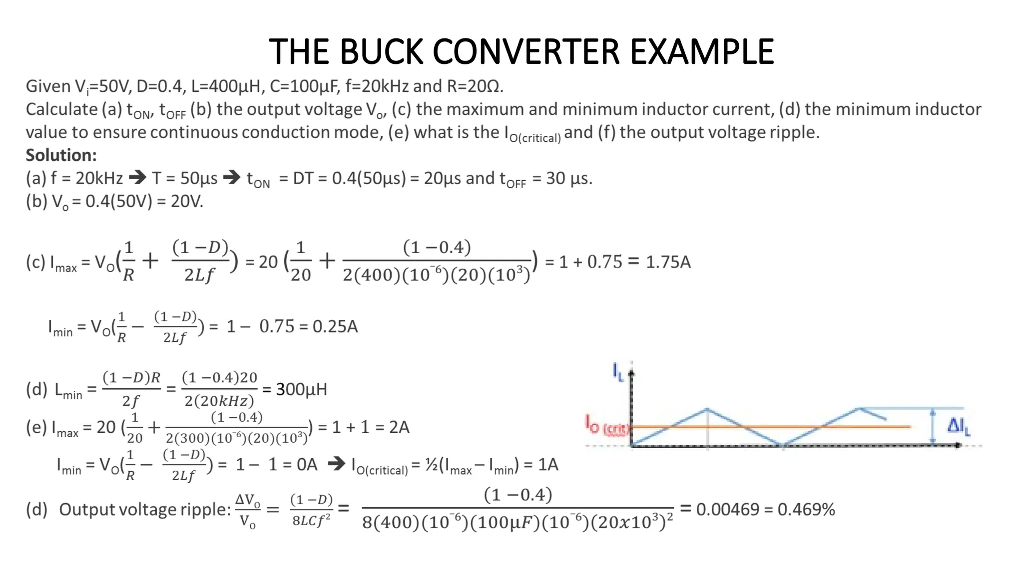
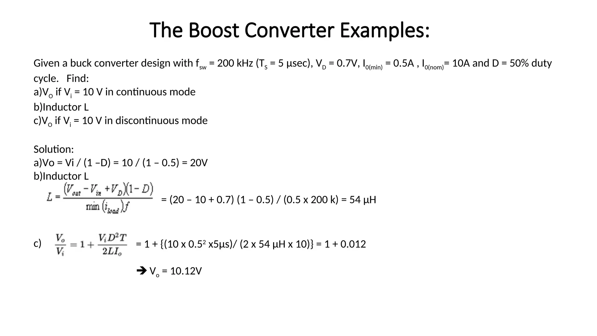
Given a buckconverter design with fsw = 200 kHz (TS = 5 μsec), VD = 0.7V, I0(min) = 0.5A , I0(nom)= 10A and D = 50% duty
cycle. Find:
a)VO if Vi = 10 V in continuous mode
b)Inductor L
c)VO if Vi = 10 V in discontinuous mode
Solution:
a)Vo = Vi / (1 –D) = 10 / (1 – 0.5) = 20V
b)Inductor L
c)
= (20 – 10 + 0.7) (1 – 0.5) / (0.5 x 200 k) = 54 µH
= 1 + {(10 x 0.52
x5µs)/ (2 x 54 µH x 10)} = 1 + 0.012
Vo = 10.12V
The Boost Converter Examples:
32.
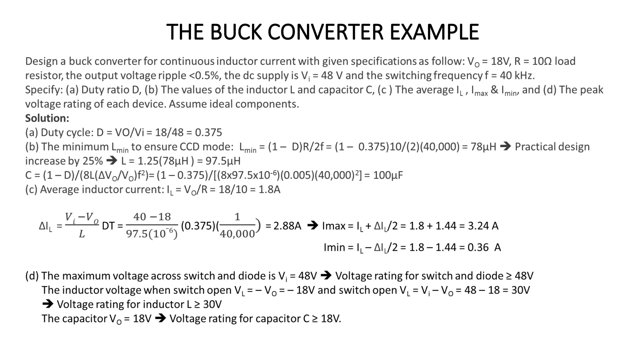
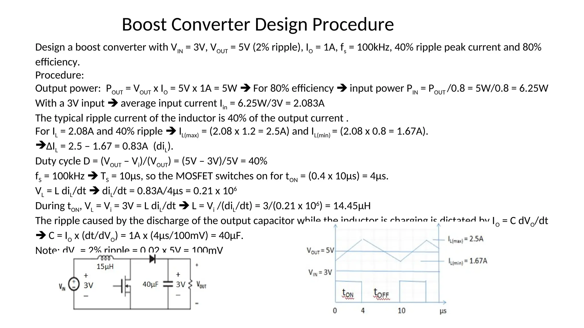
Design a boostconverter with VIN = 3V, VOUT = 5V (2% ripple), IO = 1A, fs = 100kHz, 40% ripple peak current and 80%
efficiency.
Procedure:
Output power: POUT = VOUT x IO = 5V x 1A = 5W For 80% efficiency input power PIN = POUT /0.8 = 5W/0.8 = 6.25W
With a 3V input average input current Iin = 6.25W/3V = 2.083A
The typical ripple current of the inductor is 40% of the output current .
For IL = 2.08A and 40% ripple IL(max) = (2.08 x 1.2 = 2.5A) and IL(min) = (2.08 x 0.8 = 1.67A).
ΔIL = 2.5 – 1.67 = 0.83A (diL).
Duty cycle D = (VOUT – Vi)/(VOUT) = (5V – 3V)/5V = 40%
fS = 100kHz TS = 10µs, so the MOSFET switches on for tON = (0.4 x 10µs) = 4µs.
VL = L diL/dt diL/dt = 0.83A/4µs = 0.21 x 10⁶
During tON, VL = Vi = 3V = L diL/dt L = Vi /(diL/dt) = 3/(0.21 x 106
) = 14.45µH
The ripple caused by the discharge of the output capacitor while the inductor is charging is dictated by IO = C dVO/dt
C = IO x (dt/dVO) = 1A x (4µs/100mV) = 40µF.
Note: dVO = 2% ripple = 0.02 x 5V = 100mV
Boost Converter Design Procedure
33.
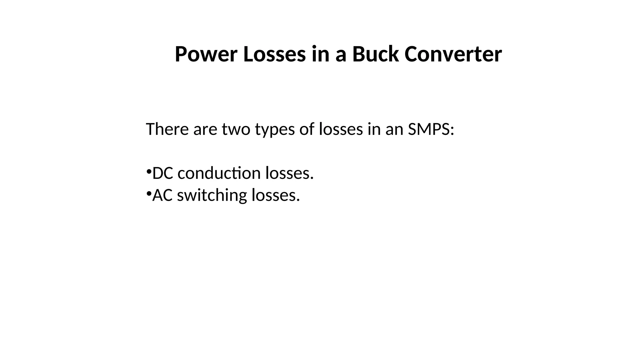
Power Losses ina Buck Converter
There are two types of losses in an SMPS:
•DC conduction losses.
•AC switching losses.
34.
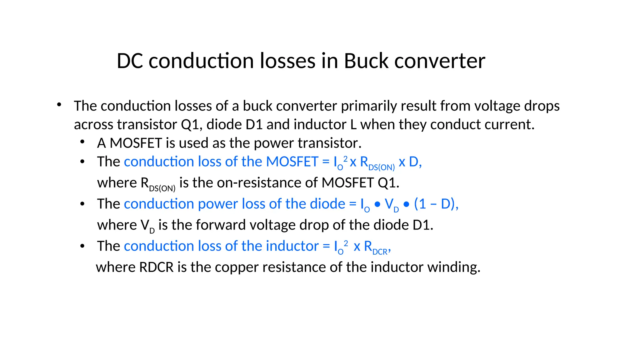
• The conductionlosses of a buck converter primarily result from voltage drops
across transistor Q1, diode D1 and inductor L when they conduct current.
• A MOSFET is used as the power transistor.
• The conduction loss of the MOSFET = IO
2
x RDS(ON) x D,
where RDS(ON) is the on-resistance of MOSFET Q1.
• The conduction power loss of the diode = IO • VD • (1 – D),
where VD is the forward voltage drop of the diode D1.
• The conduction loss of the inductor = IO
2
x RDCR,
where RDCR is the copper resistance of the inductor winding.
DC conduction losses in Buck converter
35.
Therefore, the conductionloss of the buck converter is approximately:
PCON_LOSS = (IO
2
x RDS(ON) x D) + (IO • VD • [1 – D]) + (IO
2
x RDCR)
Power Losses in a Buck Converter
Considering only conduction loss, the converter efficiency is:
Example:
For 12V input buck supply 3.3V/10AMAX output buck supply.
•Use 27.5% duty cycle provides a 3.3V output voltage.
Vout = Vin x D = 12 x 0.275 = 3.3 V
•MOSFET RDS(ON) = 10 mΩ
•Diode forward voltage VD = 0.5V (freewheeling diode)
•Inductor RDCR = 2 mΩ
Conduction loss at full load:
PCON_LOSS = (IO
2
x RDS(ON) x D) + (IO x VD x [1 – D]) + (IO
2
x RDCR)
= (102
x 0.01 x 0.275) + (10 x 0.5 x [1 – 0.275]) + (102
x 0.002)
= 0.275W + 3.62W + 0.2W = 4.095W
Buck converter efficiency:
36.
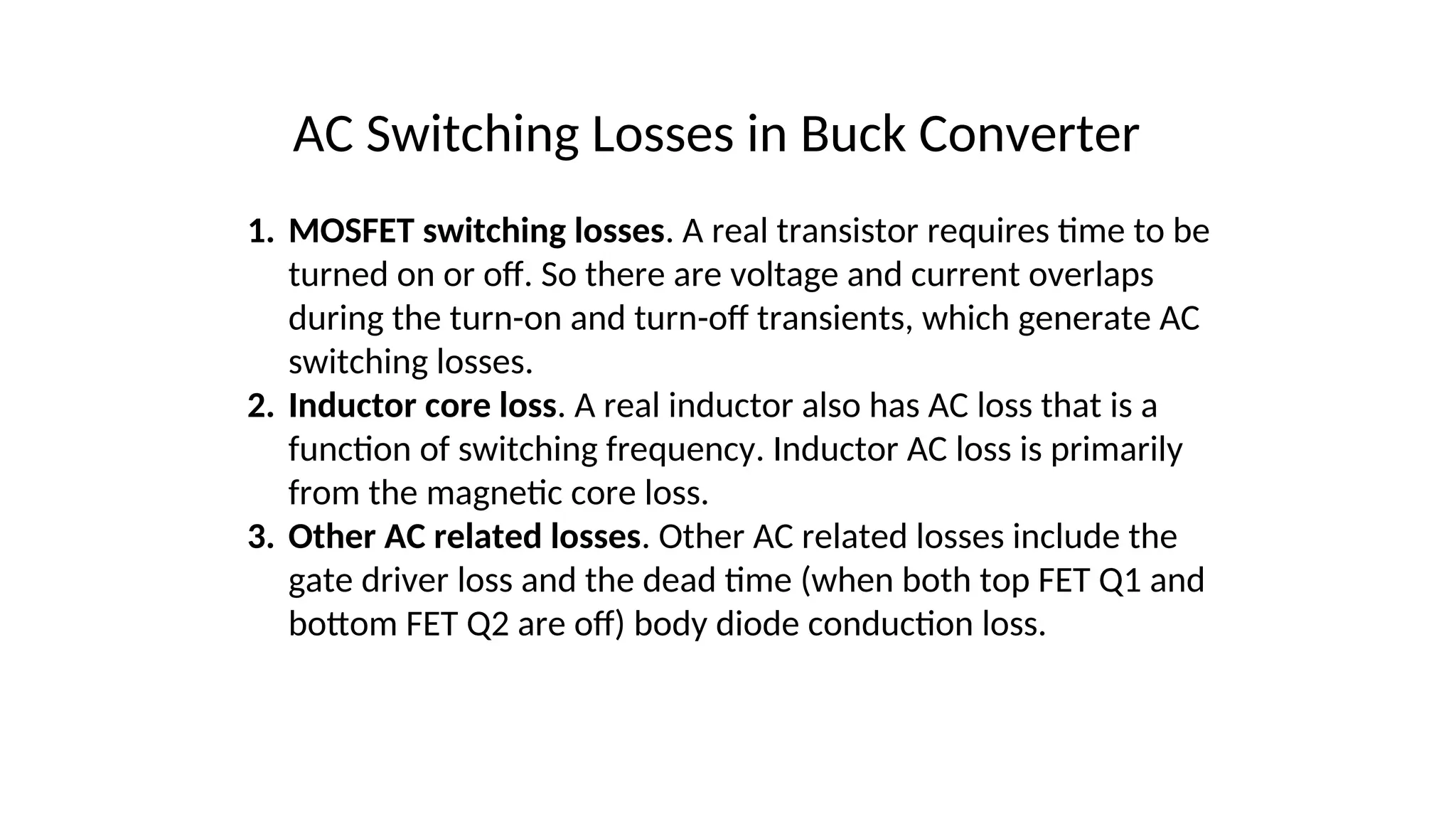
AC Switching Lossesin Buck Converter
1. MOSFET switching losses. A real transistor requires time to be
turned on or off. So there are voltage and current overlaps
during the turn-on and turn-off transients, which generate AC
switching losses.
2. Inductor core loss. A real inductor also has AC loss that is a
function of switching frequency. Inductor AC loss is primarily
from the magnetic core loss.
3. Other AC related losses. Other AC related losses include the
gate driver loss and the dead time (when both top FET Q1 and
bottom FET Q2 are off) body diode conduction loss.
37.
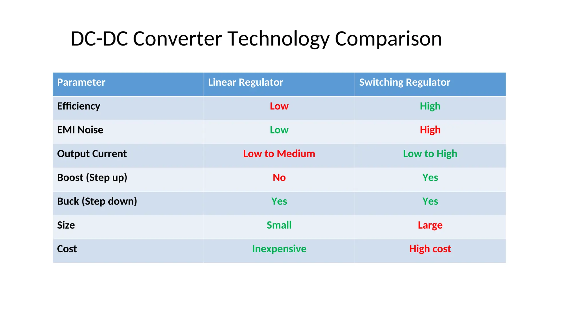
Parameter Linear RegulatorSwitching Regulator
Efficiency Low High
EMI Noise Low High
Output Current Low to Medium Low to High
Boost (Step up) No Yes
Buck (Step down) Yes Yes
Size Small Large
Cost Inexpensive High cost
DC-DC Converter Technology Comparison
![Therefore, the conduction loss of the buck converter is approximately:
PCON_LOSS = (IO
2
x RDS(ON) x D) + (IO • VD • [1 – D]) + (IO
2
x RDCR)
Power Losses in a Buck Converter
Considering only conduction loss, the converter efficiency is:
Example:
For 12V input buck supply 3.3V/10AMAX output buck supply.
•Use 27.5% duty cycle provides a 3.3V output voltage.
Vout = Vin x D = 12 x 0.275 = 3.3 V
•MOSFET RDS(ON) = 10 mΩ
•Diode forward voltage VD = 0.5V (freewheeling diode)
•Inductor RDCR = 2 mΩ
Conduction loss at full load:
PCON_LOSS = (IO
2
x RDS(ON) x D) + (IO x VD x [1 – D]) + (IO
2
x RDCR)
= (102
x 0.01 x 0.275) + (10 x 0.5 x [1 – 0.275]) + (102
x 0.002)
= 0.275W + 3.62W + 0.2W = 4.095W
Buck converter efficiency:](https://image.slidesharecdn.com/introductiontodc-dcconversion-250325025720-29c9dcc2/75/Introduction-to-DC-DC-Conversion-how-to-design-a-dc-dc-convert-35-2048.jpg)


![Chapt_4[1].ppt very interseting and important](https://cdn.slidesharecdn.com/ss_thumbnails/chapt41-251208222956-7cf5e0fa-thumbnail.jpg?width=640&height=640&fit=bounds)


![[BROCHURE] Italy Tour Project | @SlideON](https://cdn.slidesharecdn.com/ss_thumbnails/brochure8-251215152319-2805af68-thumbnail.jpg?width=640&height=640&fit=bounds)


