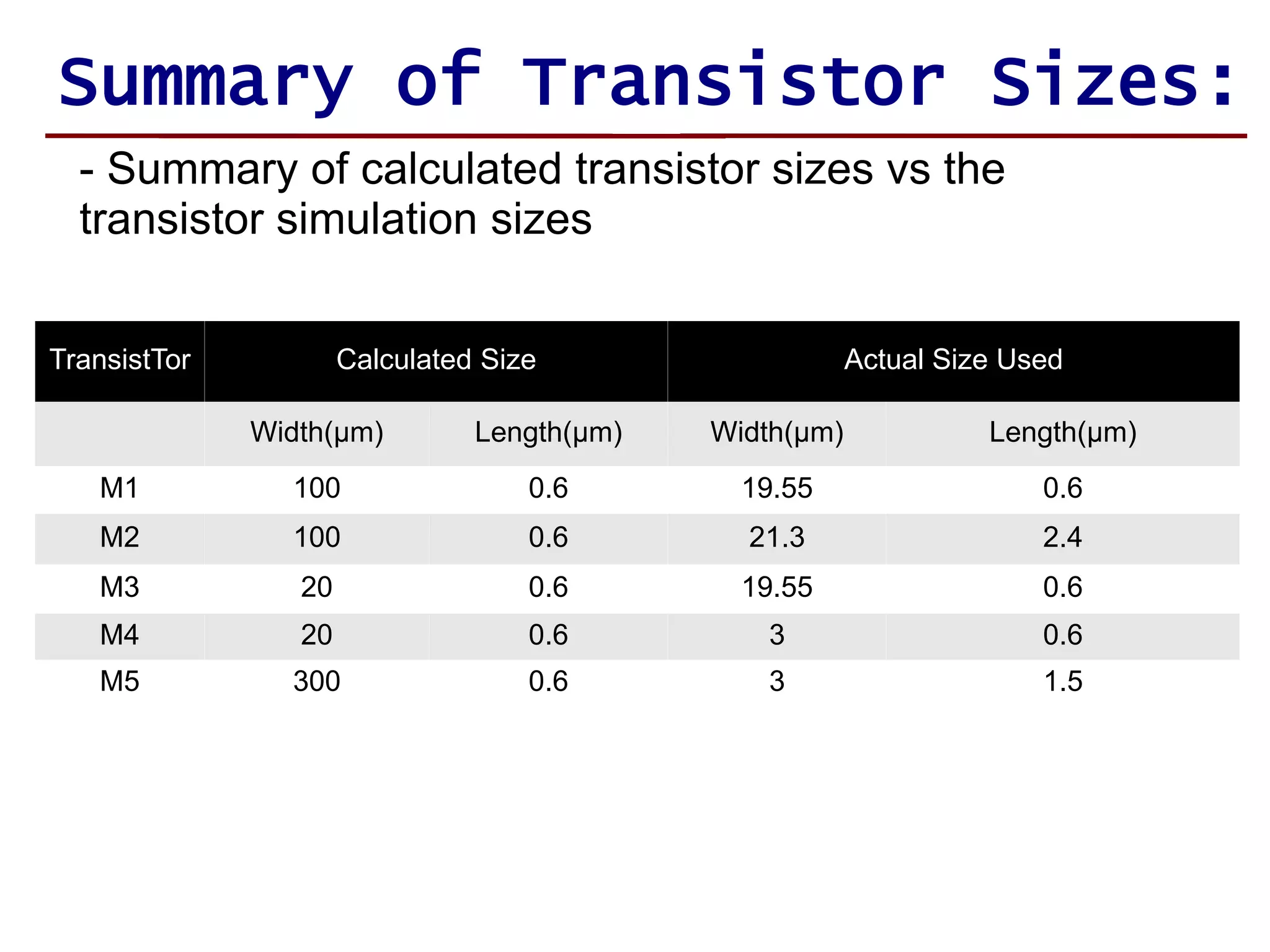
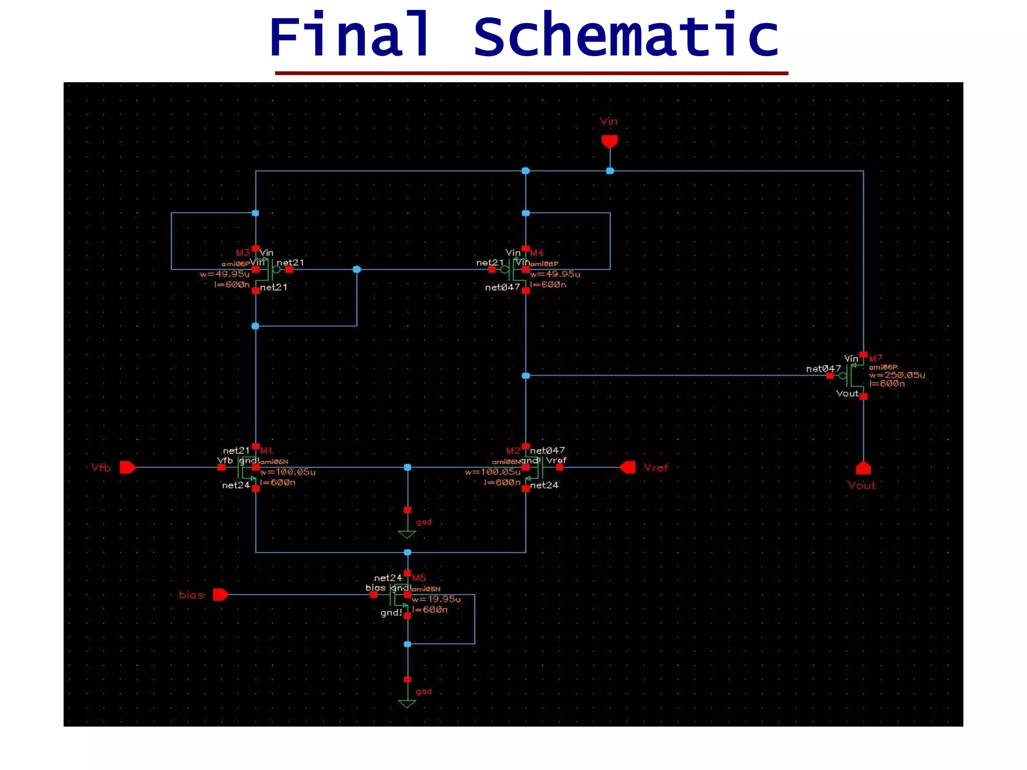
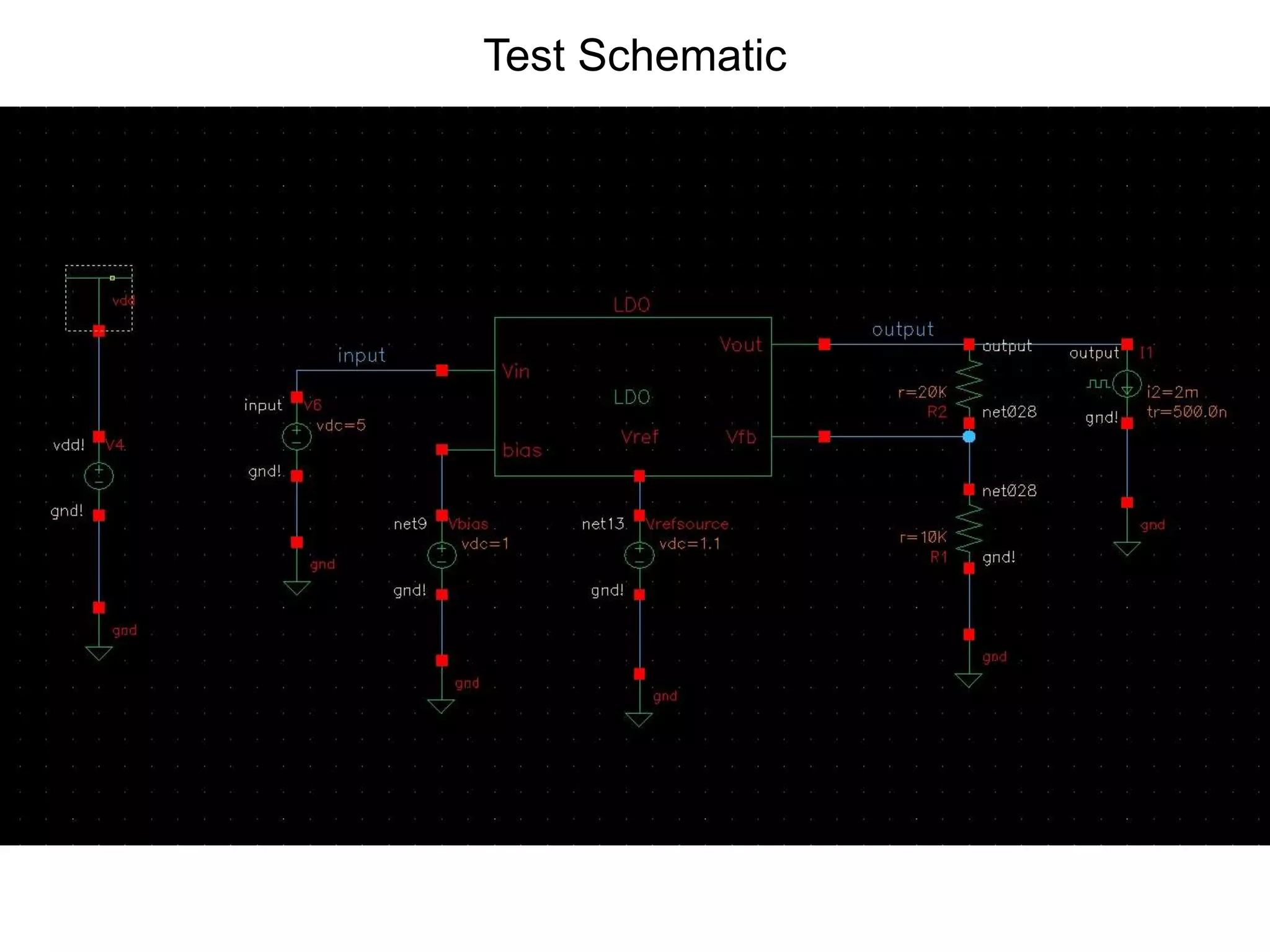
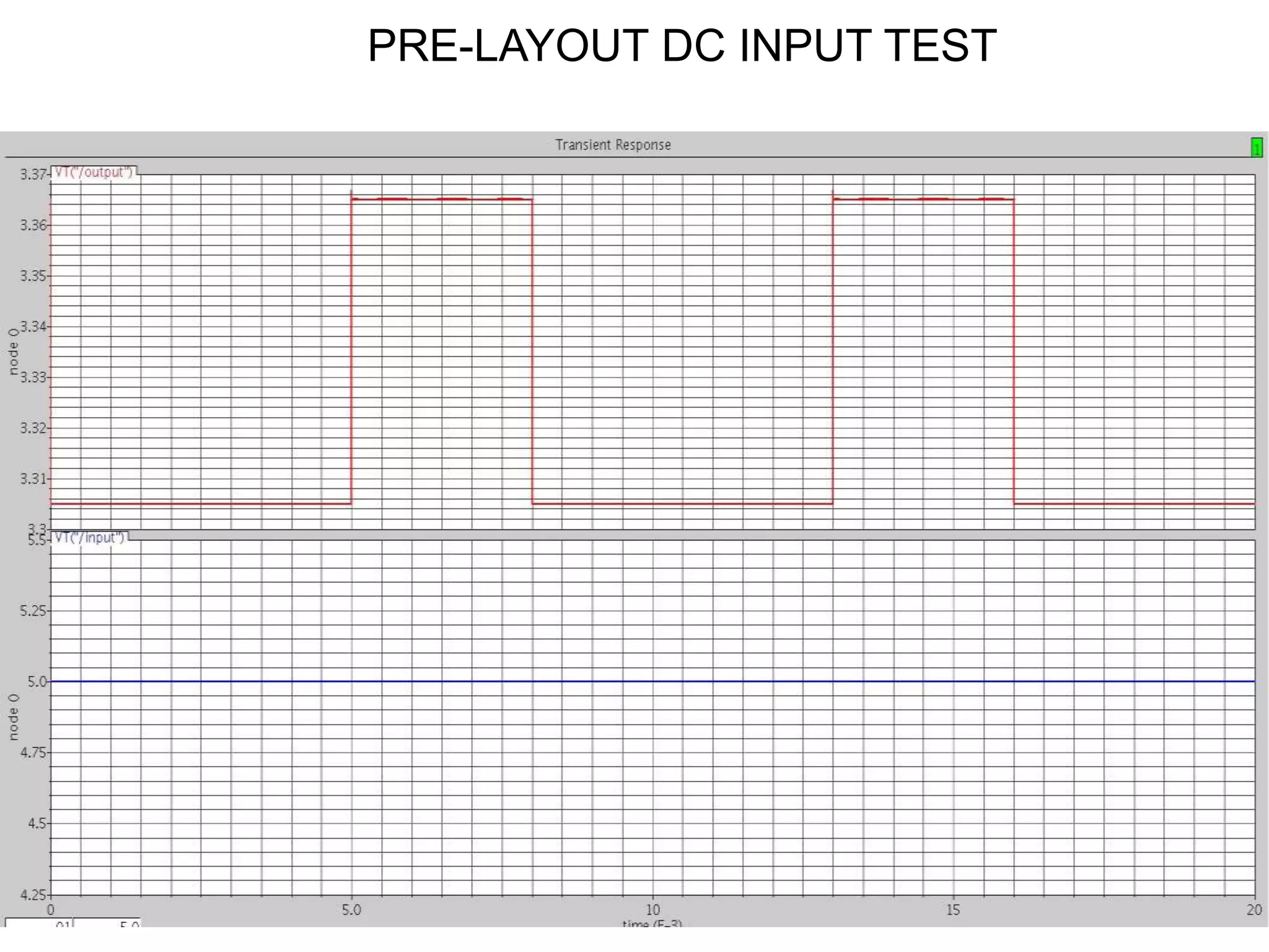
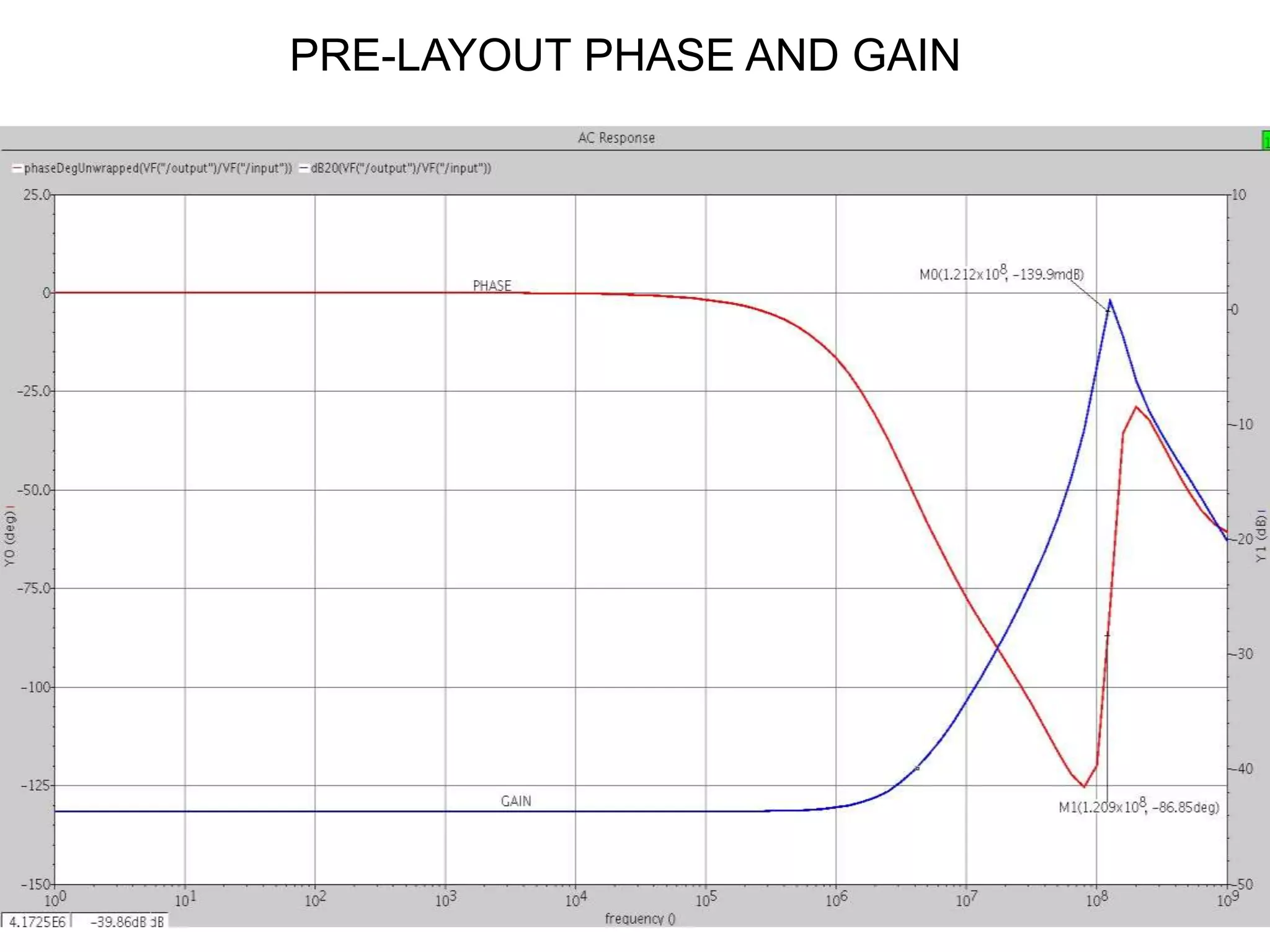
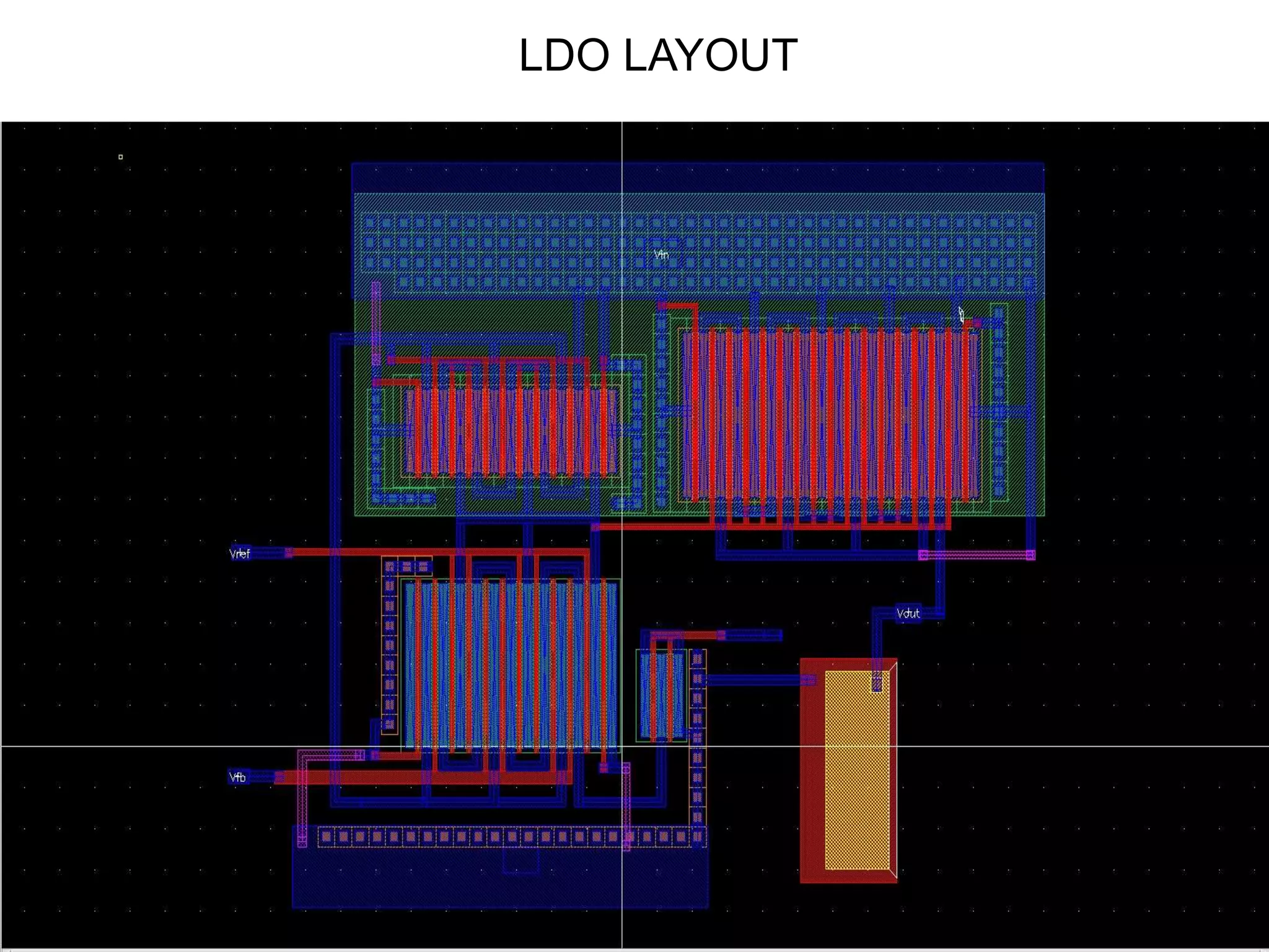
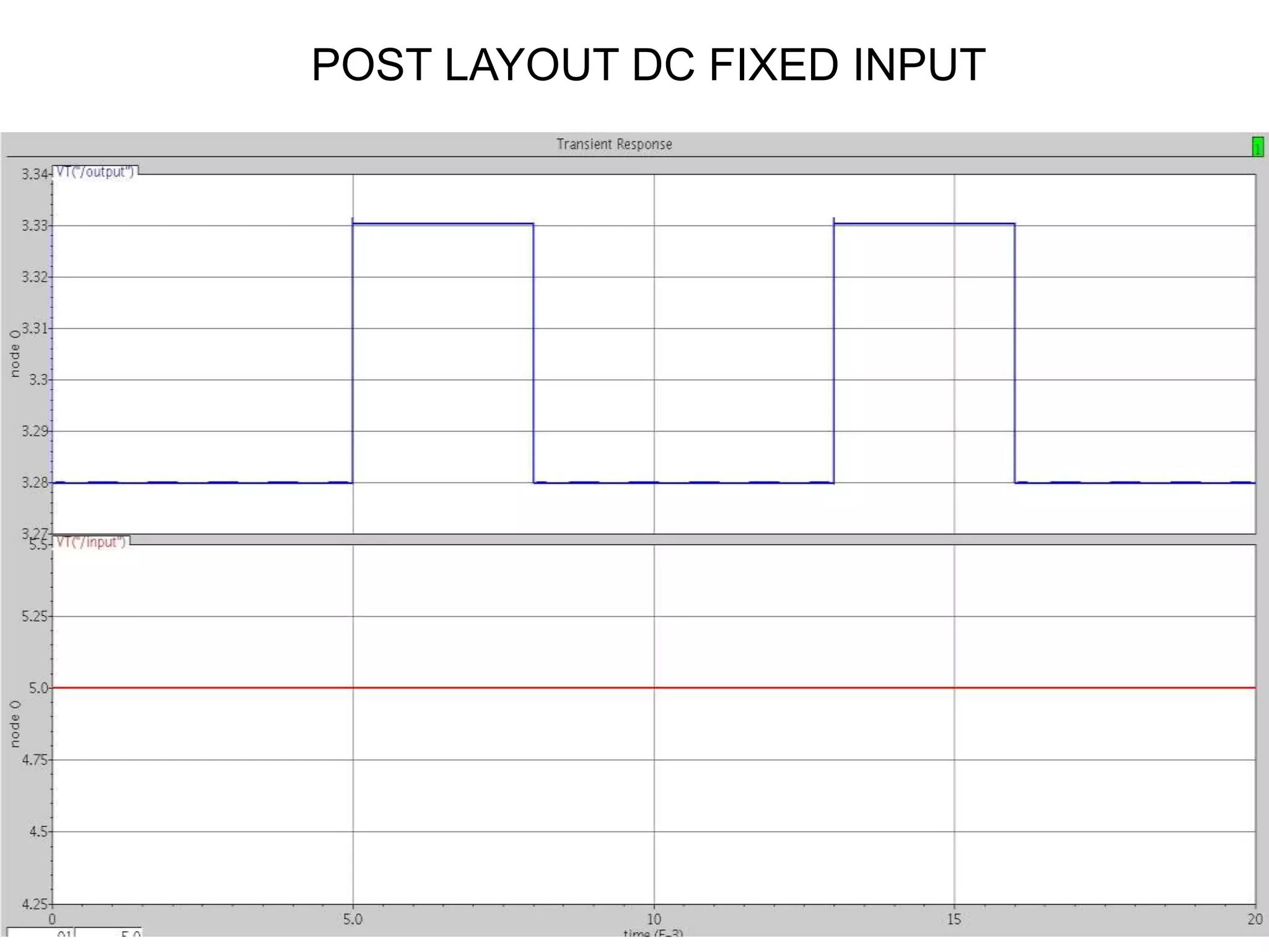
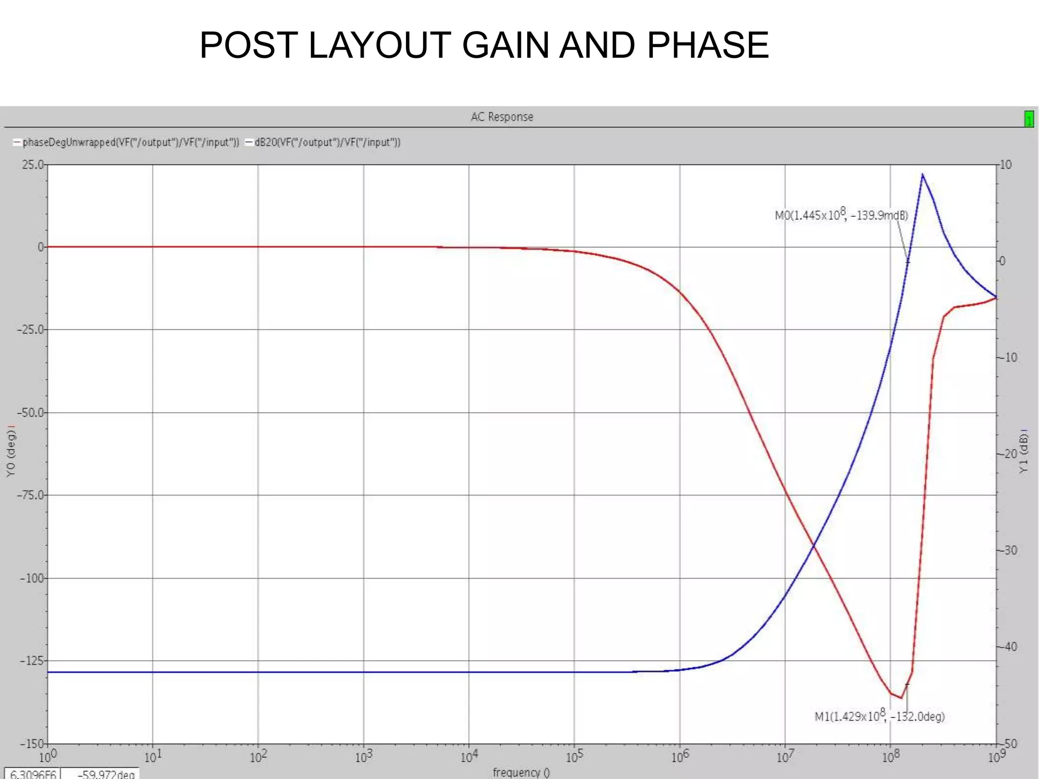
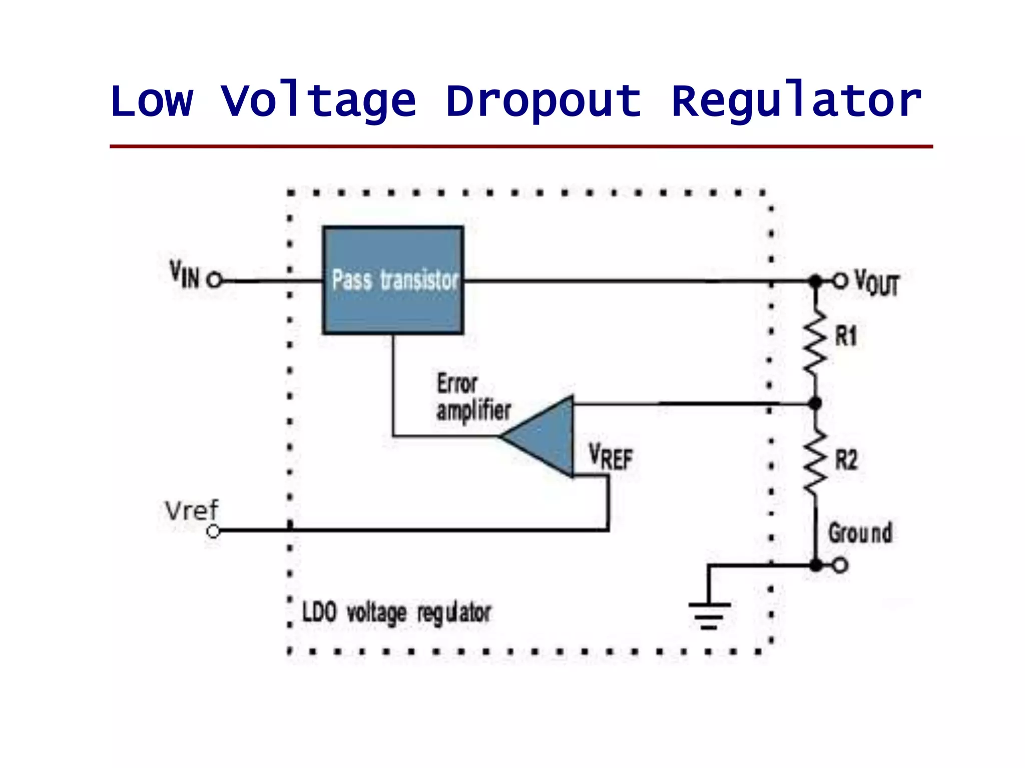
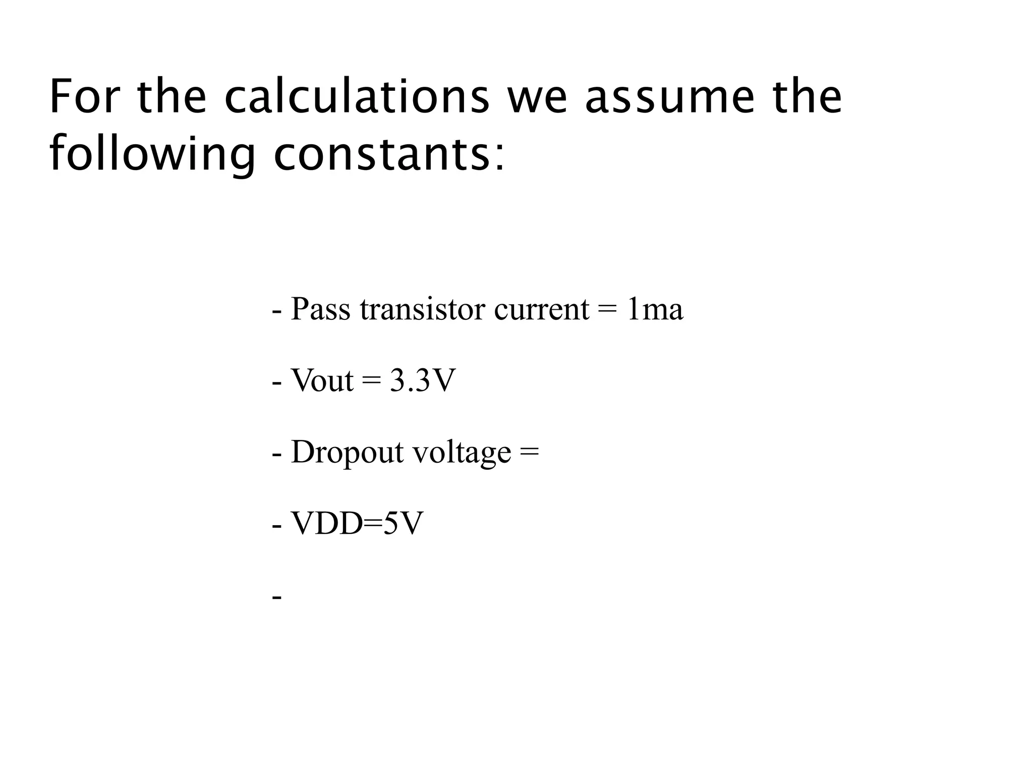
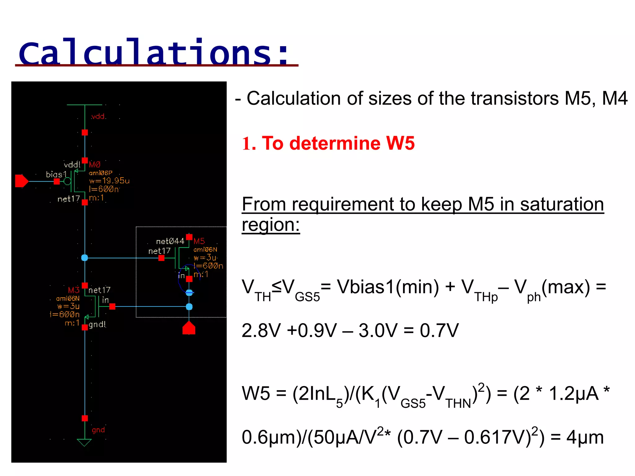
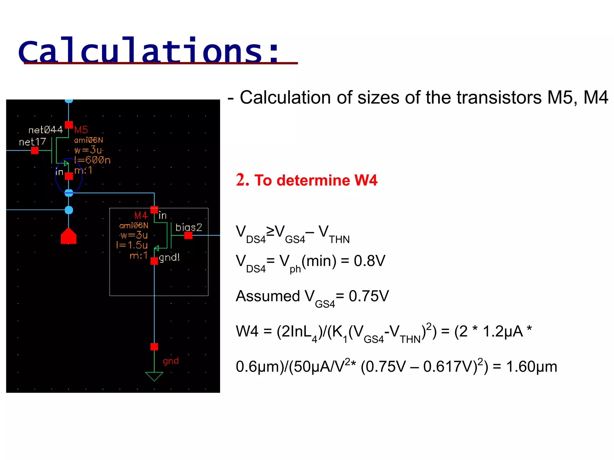
This document describes the design calculations for a low voltage dropout regulator to provide an output voltage of 3.3V from an input of 5V. It involves calculating the range of bias voltages and sizes of the transistors in the regulator circuit. Transistor widths are determined to keep transistors in saturation and ensure sufficient drive. The calculations result in transistor width and length values that are then simulated before and after layout to verify the regulator design meets specifications.
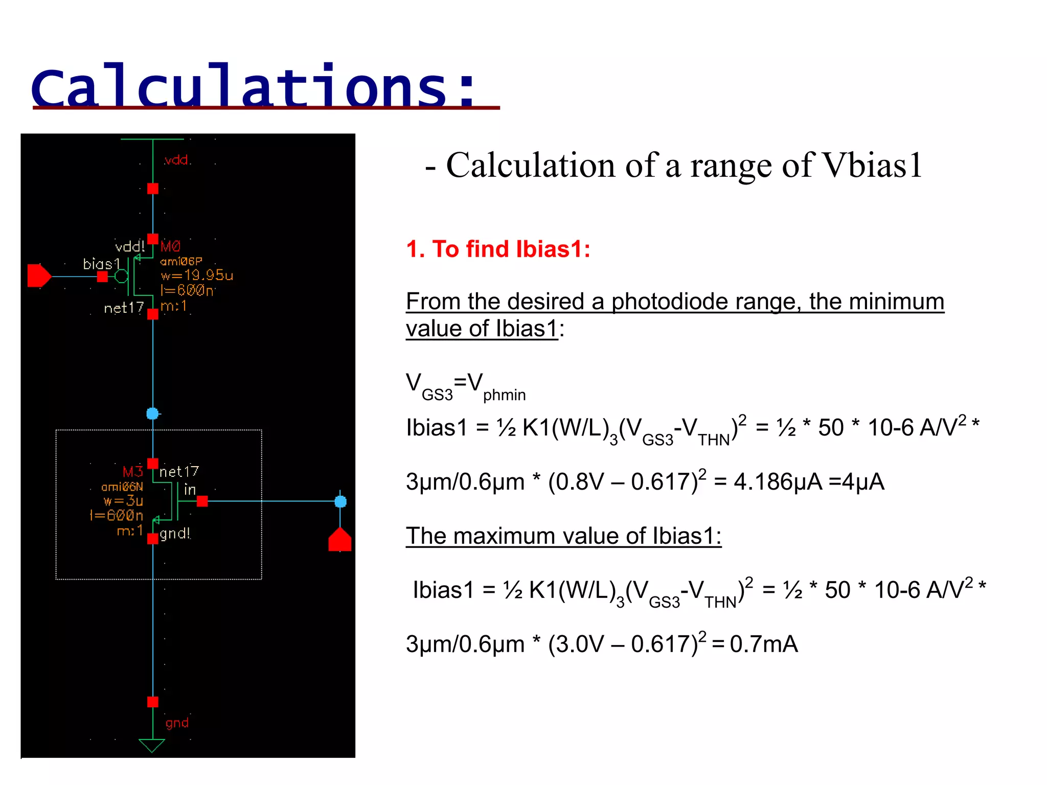
![Calculations:
- Calculation of a range of Vbias1
2. To find Vbias1:
Next we find the value of Vbias1 given by
Vbias1
= VDD
– VGS0
= VDD
- √[(2Ibias1)/(K2
(W/L)0
] –
VTHp
Vbias1
= VDD
– VGS0
= VDD
- √[
(2Ibias1)/(K2
(W/L)0
] – VTHp
p
The maximum value of Vbias1:
Vbias1(max) = 5V - √[(2*4µA)/(19.1µA/V2*
20µm/0.6µm)] – 0.915V =1.026 = 4V
The minimum value of Vbias1:
Vbias1(min) = VDD
– VGS0
= 5V- √[(2*0.7*10-3
)/25*
10-6
/V2 * 20µm/0.6µm) – 0.915V = 2.8V](https://image.slidesharecdn.com/4eec4f6d-bfbd-45d6-9055-5231a19bf6c3-150702203949-lva1-app6891/75/LDO-project-5-2048.jpg)
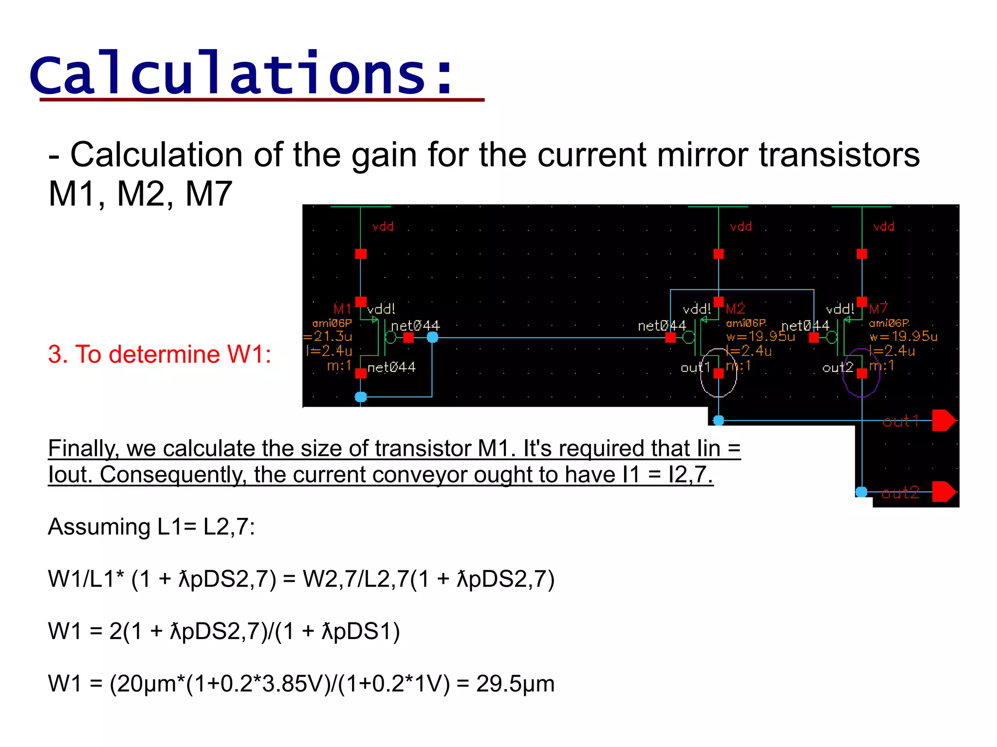
![Calculations:
- Calculation of the gain for the current mirror transistors
M1, M2, M7
1. To find VGS
for M1, M2, M7
VGS1
= VDS1
= VGS2
= VGS1
= √[(2Iout)/(K2
(W/L)2,7
] + VTHp
= √(2 *
1.2µA)/(25µA/V2
* (20/2.4)) + 0.915V = 0.107V + 0.915V = 1V](https://image.slidesharecdn.com/4eec4f6d-bfbd-45d6-9055-5231a19bf6c3-150702203949-lva1-app6891/75/LDO-project-8-2048.jpg)
![Calculations:
- Calculation of the gain for the current mirror transistors
M1, M2, M7
2. To find VDS
for current mirror:
Next we find VDS2
and VDS7
(which are the same in value)
VDS2,7
= VDD
– VDS6
= VDD
- √[(2Iout)/(K1
(W/L)6
] - VTHN
=
5V - √(2 * 1.2µA)/(50µA/V2
* (1.5/8.55)) - 0.617V = 3.85V](https://image.slidesharecdn.com/4eec4f6d-bfbd-45d6-9055-5231a19bf6c3-150702203949-lva1-app6891/75/LDO-project-9-2048.jpg)