Downloaded 1,314 times
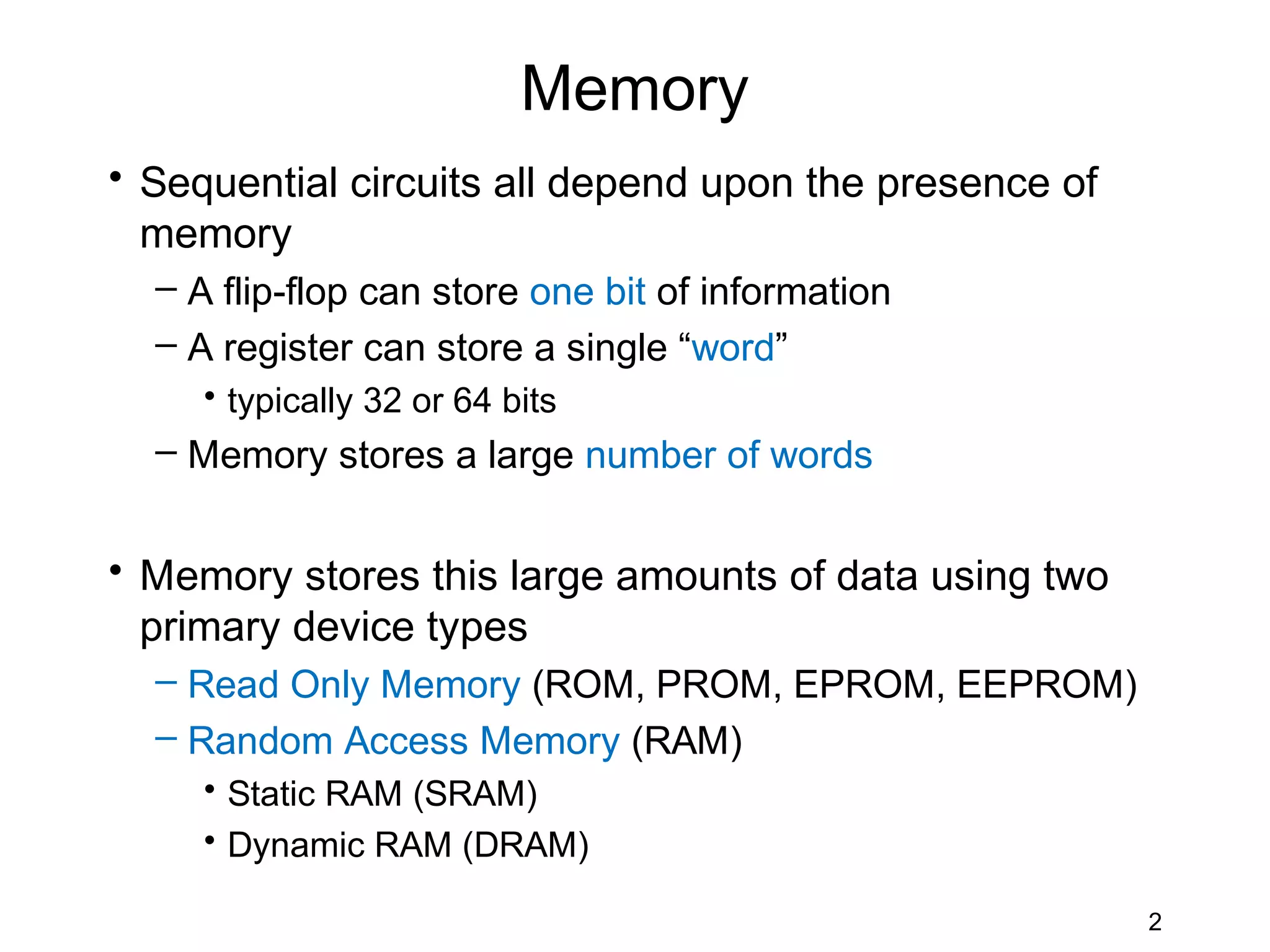

The document discusses various types of memory used in digital systems, including Read-Only Memory (ROM), Programmable ROM (PROM), Erasable Programmable ROM (EPROM), and Random Access Memory (RAM). It explains how memory is structured, addressed, and connected to the CPU, along with timing characteristics and advantages/disadvantages of ROM. The content also covers methods of programming and the function of ROM in storing data permanently without the ability to modify it during typical operation.
Overview of EET 3350 Digital Systems Design and the textbook reference including focus on Memory.
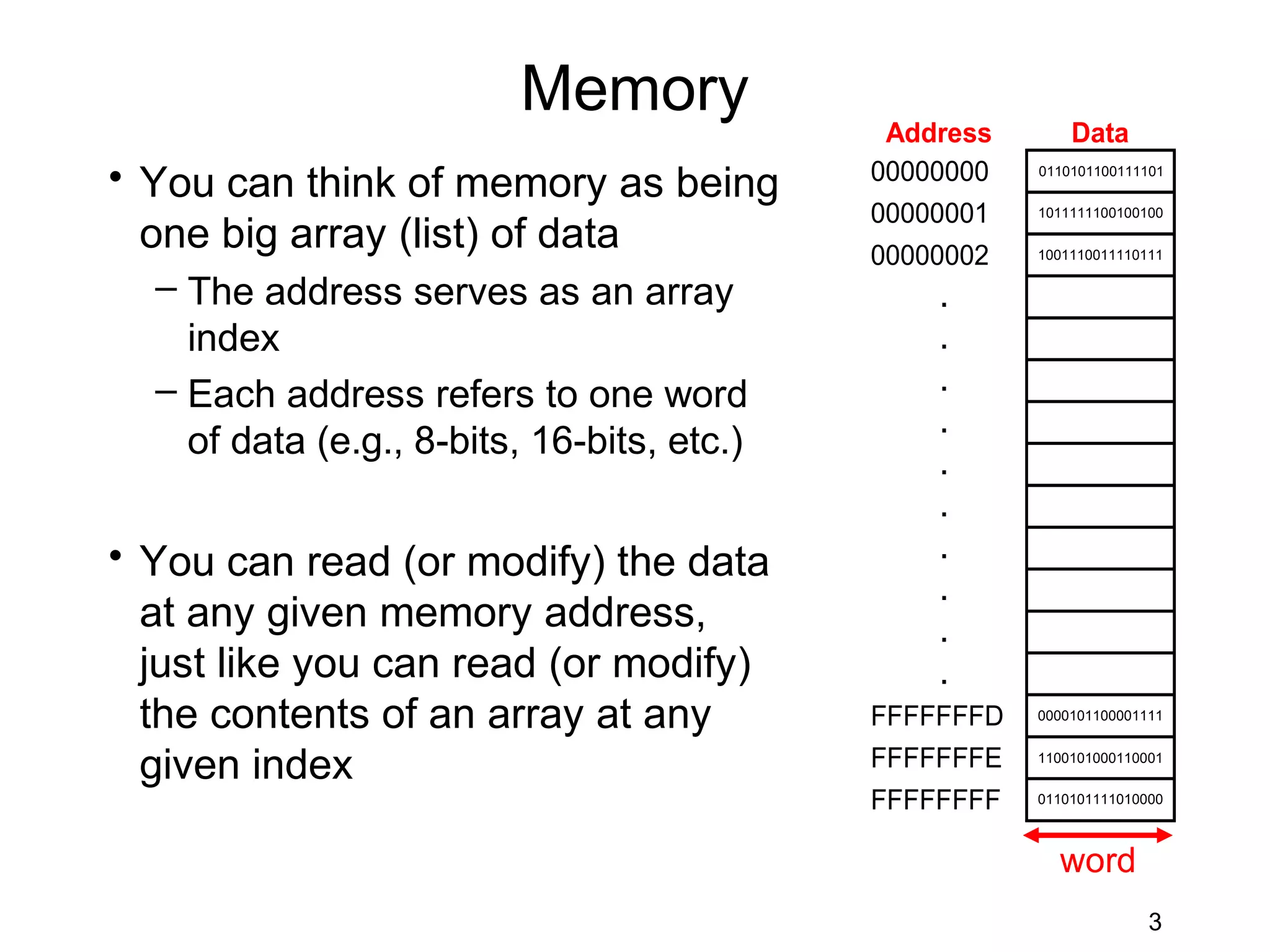
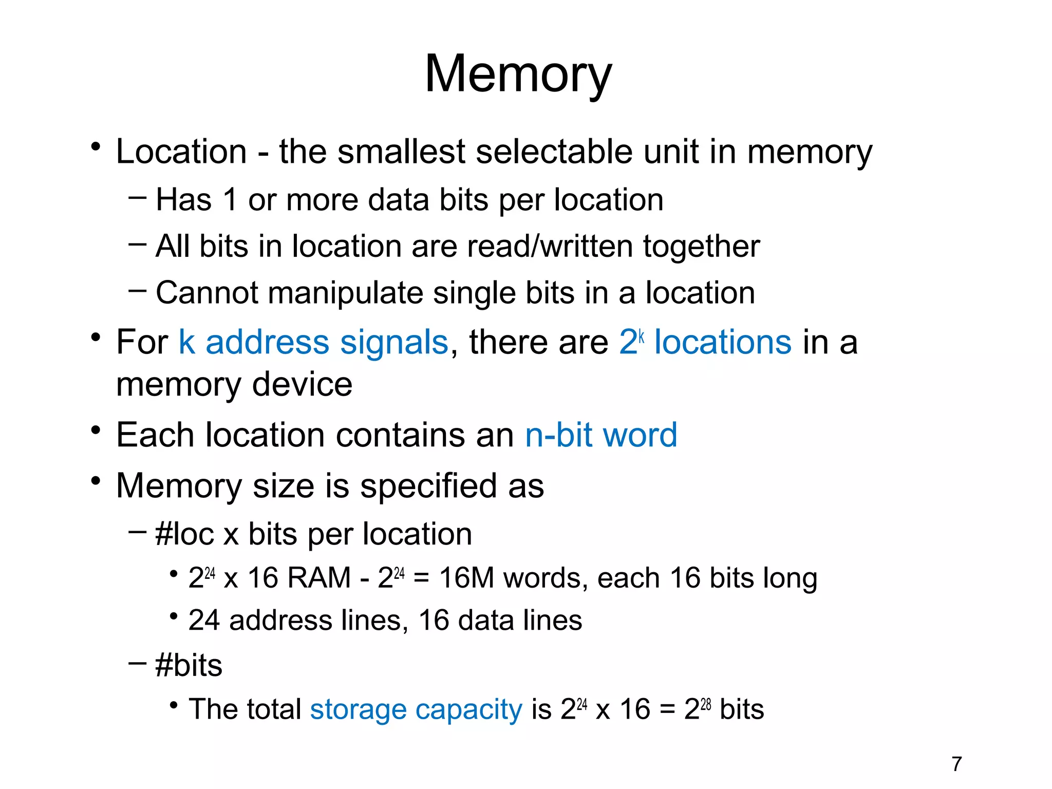
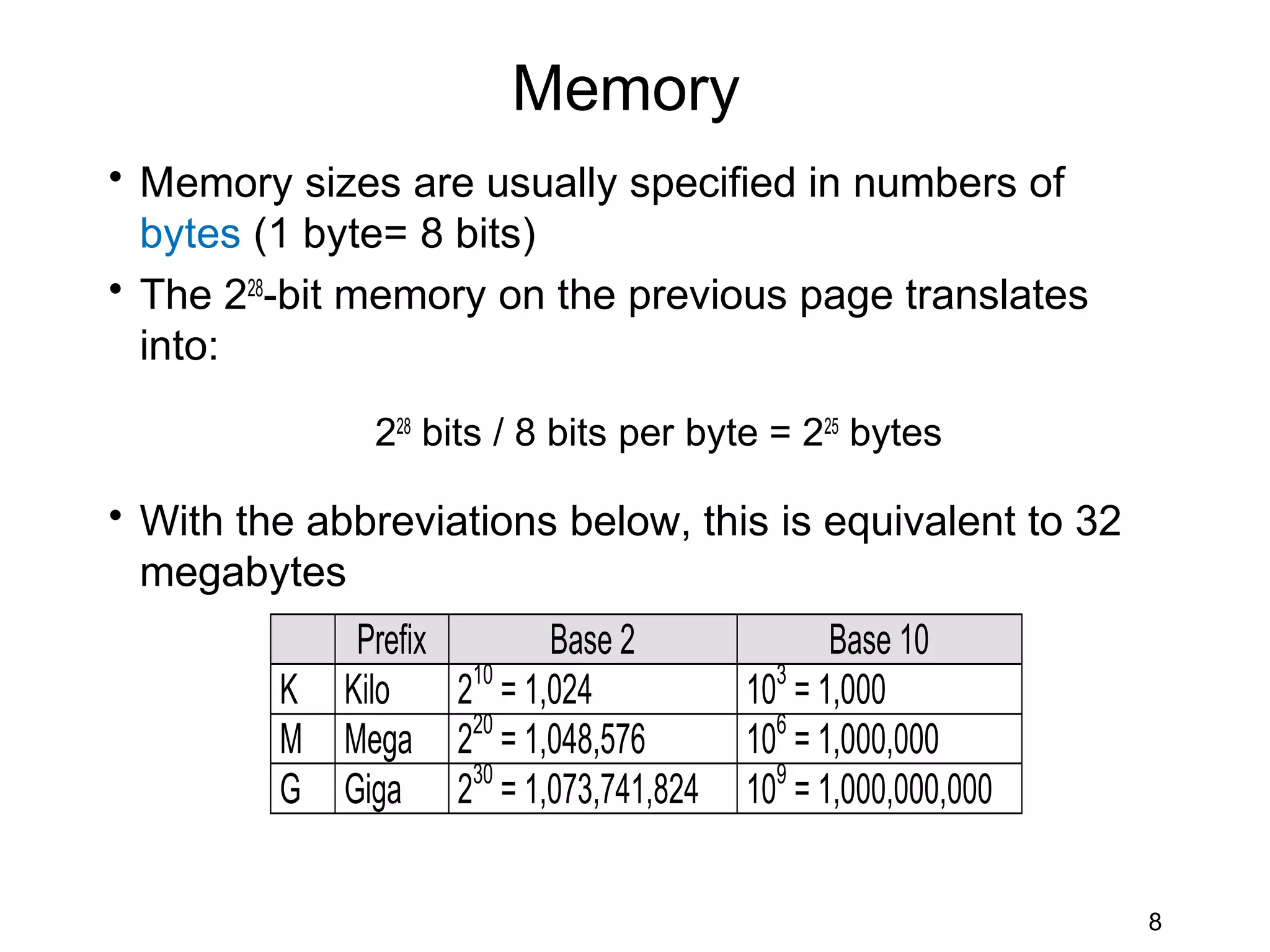
Explanation of memory types (ROM, RAM, etc.), their functions, and data structure in memory, including addresses and organization.Definition of memory locations, calculation of memory size and types specified in bits, bytes, and megabytes.
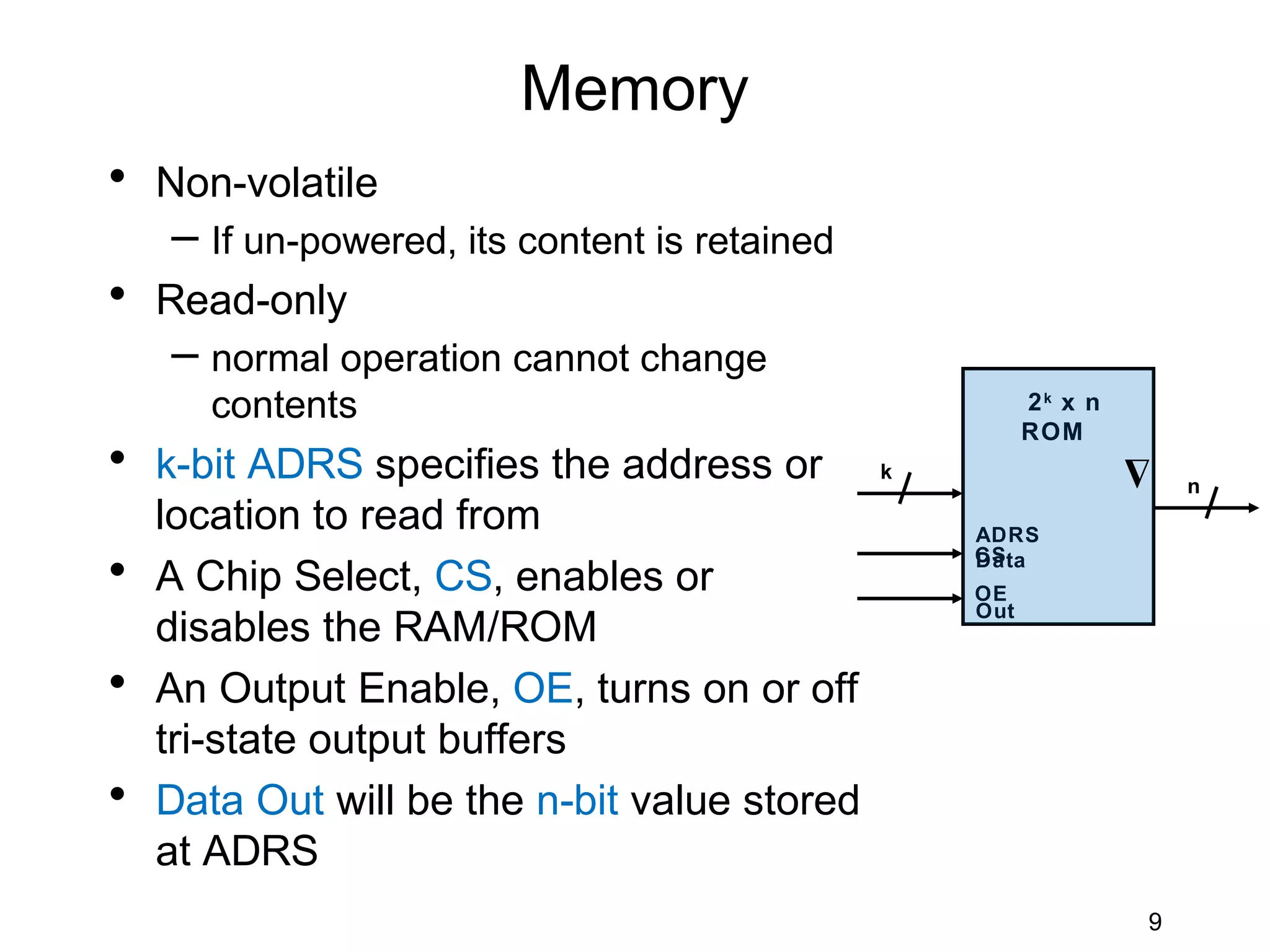
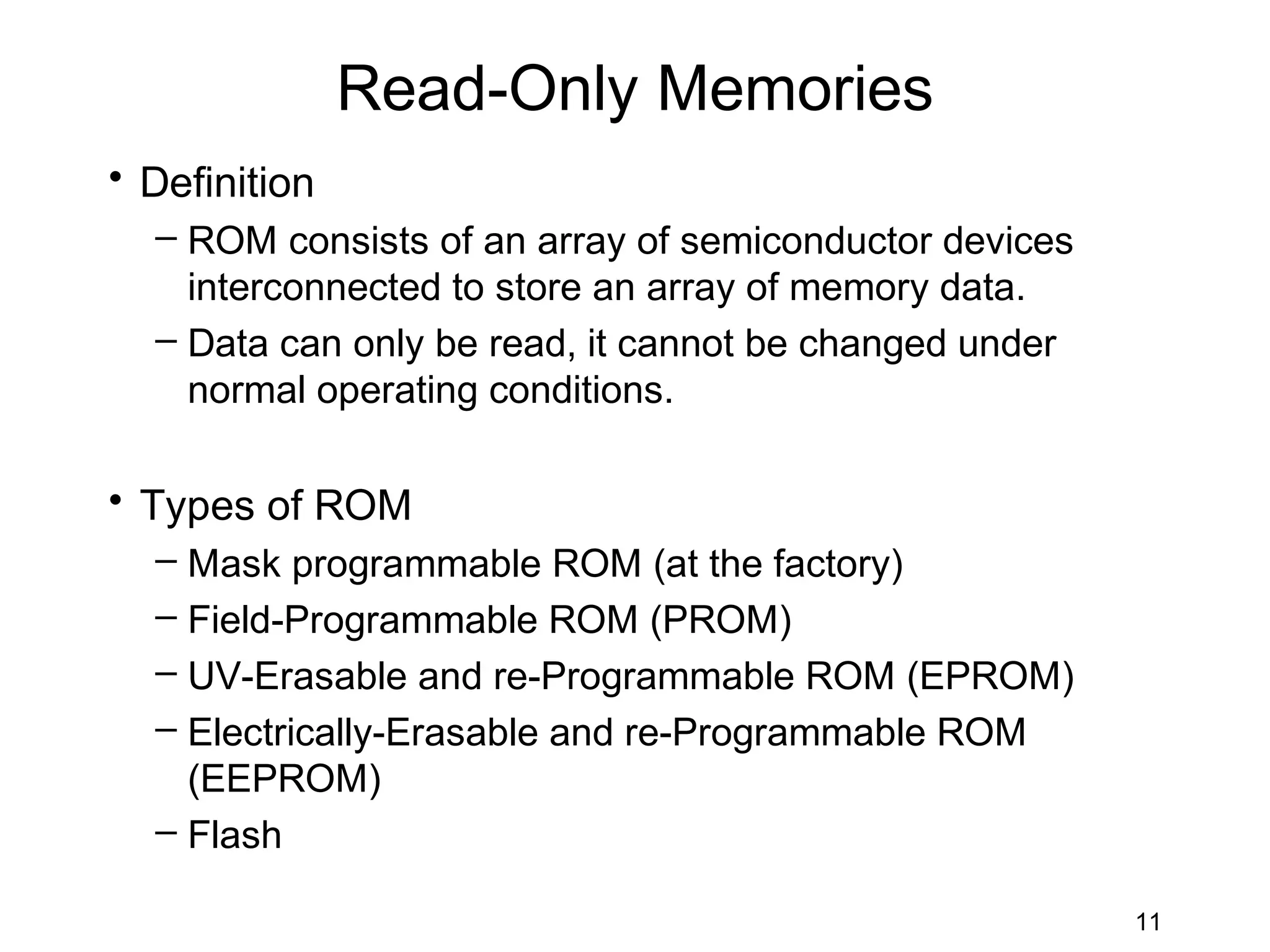
Explains ROM definitions, types, and characteristics, focusing on non-volatile and read-only nature.
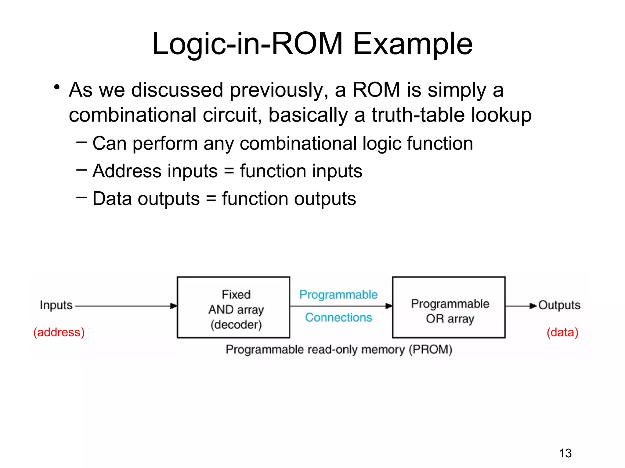
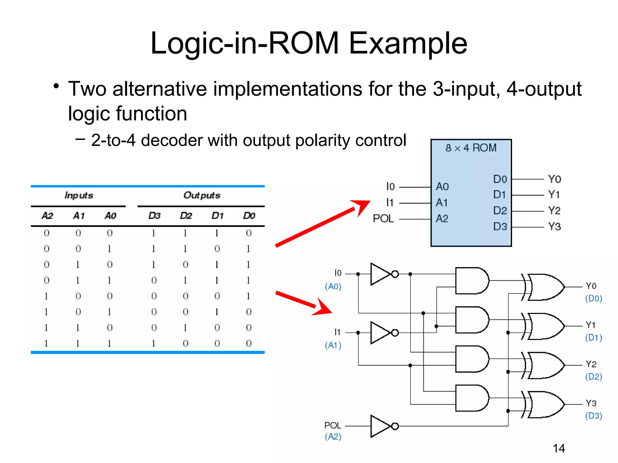
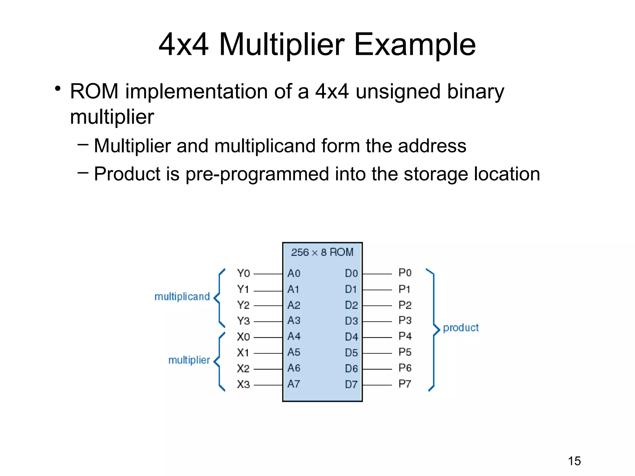
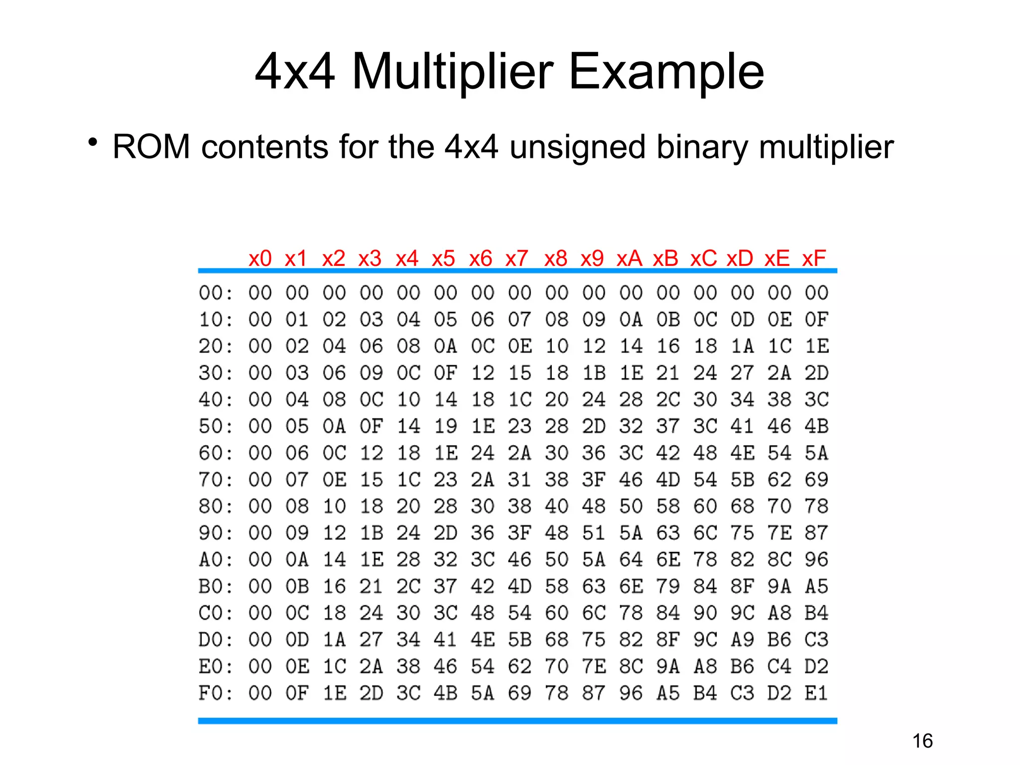
Examples of logic in ROM including combinational logic functions and implementation of a binary multiplier.
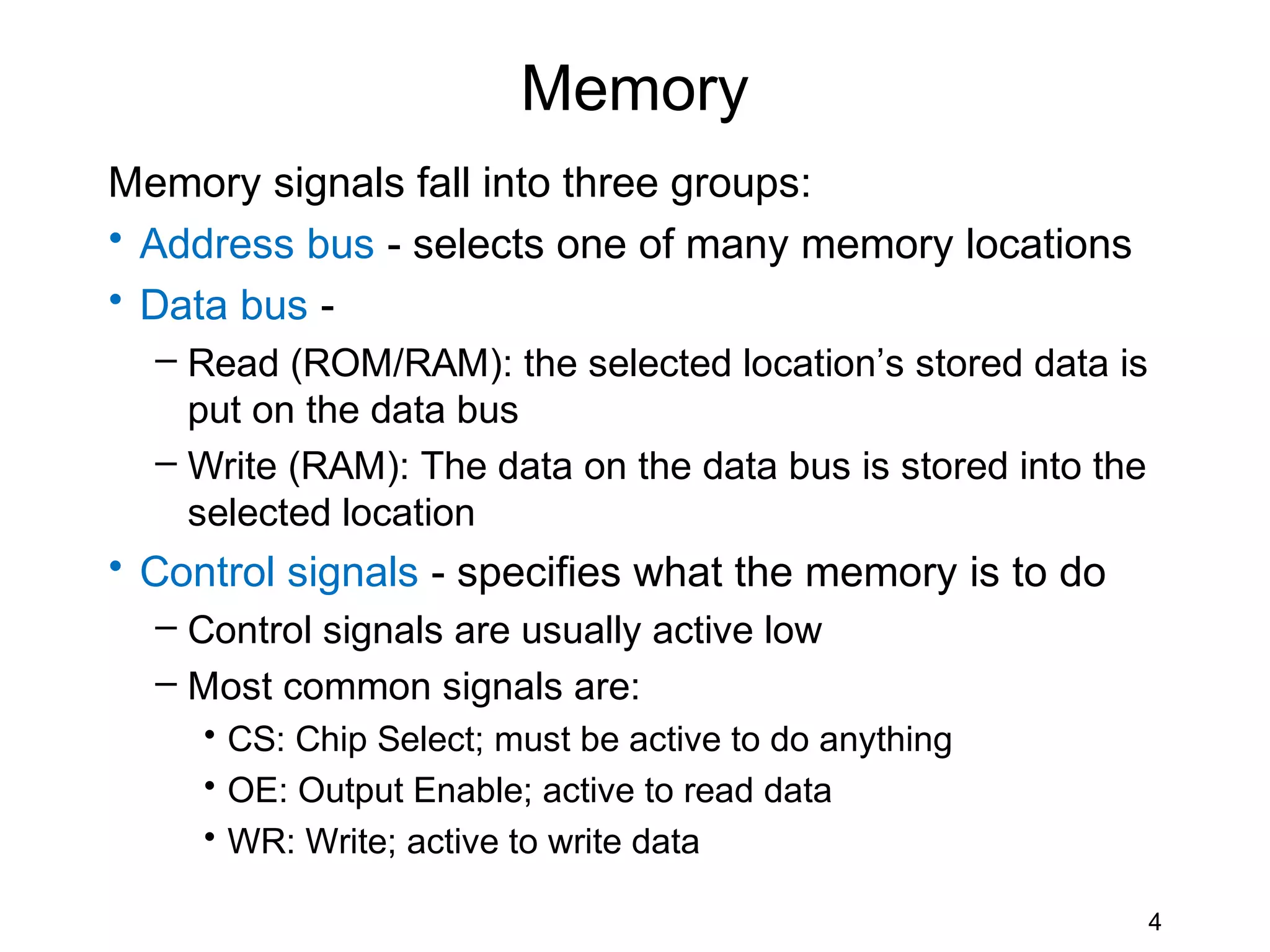
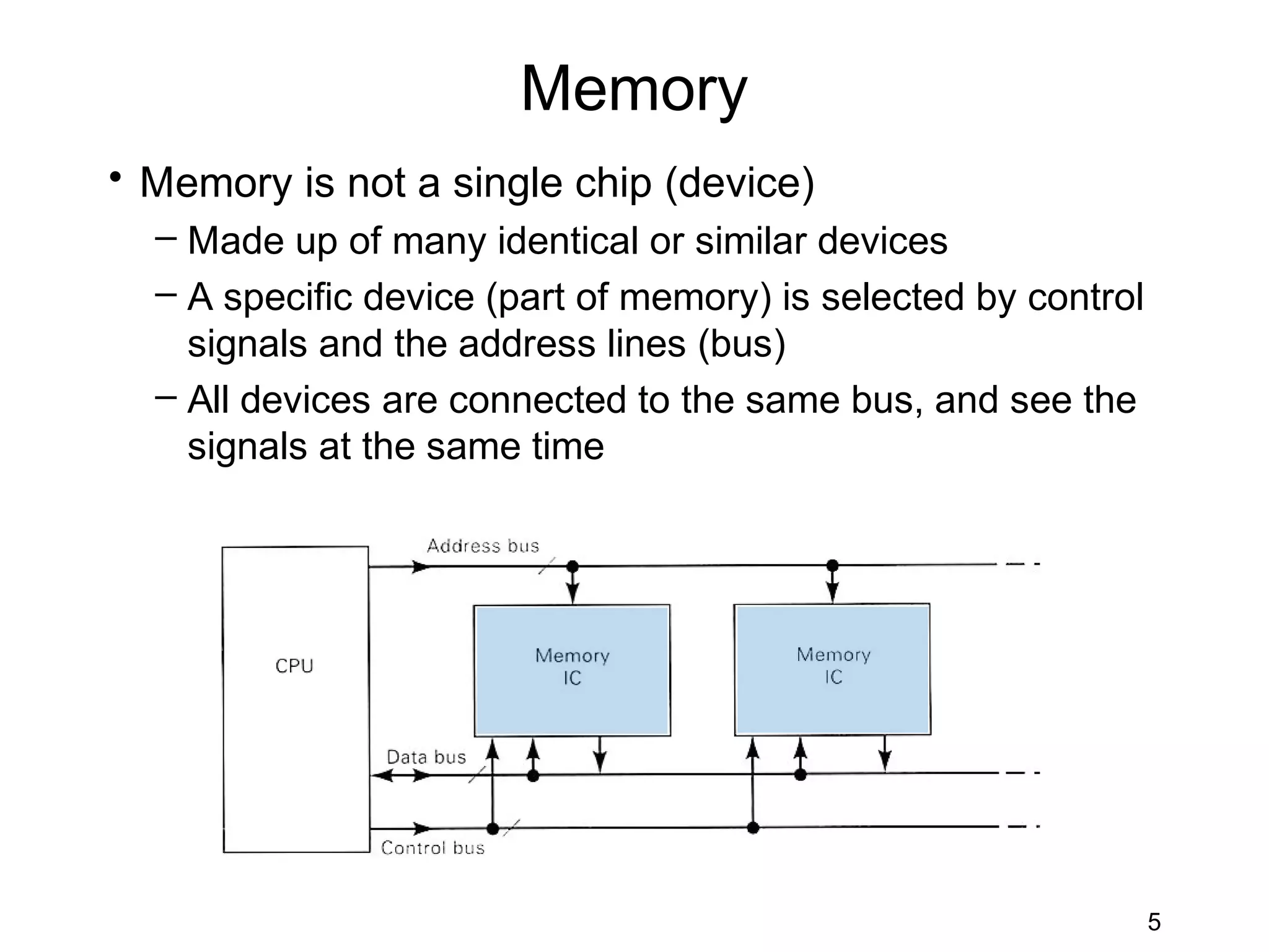
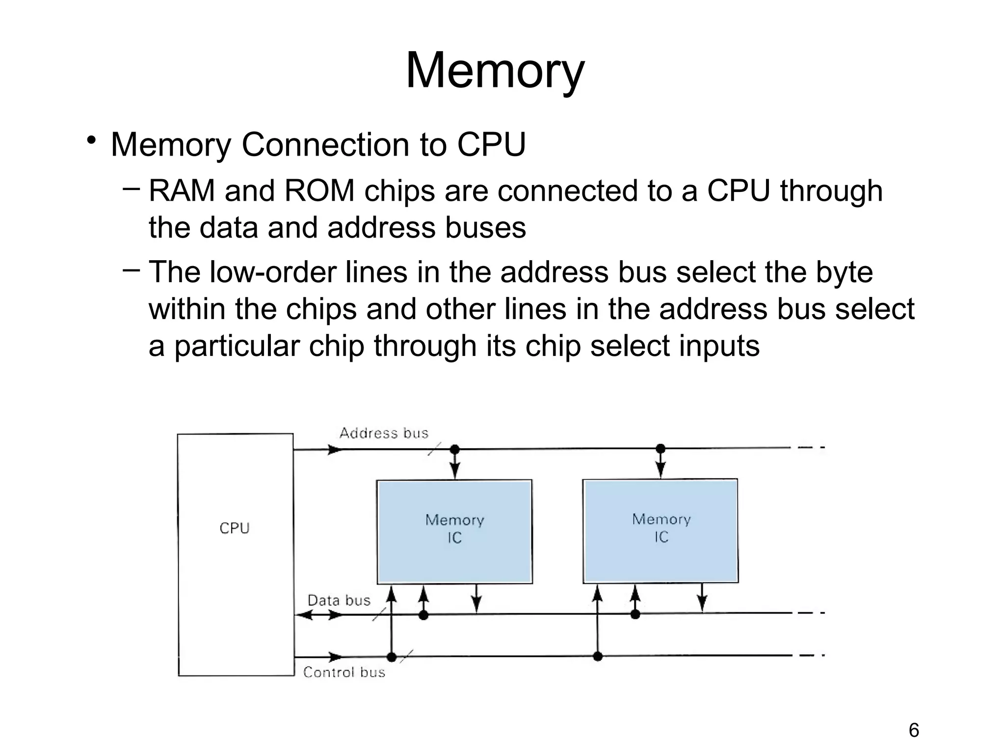
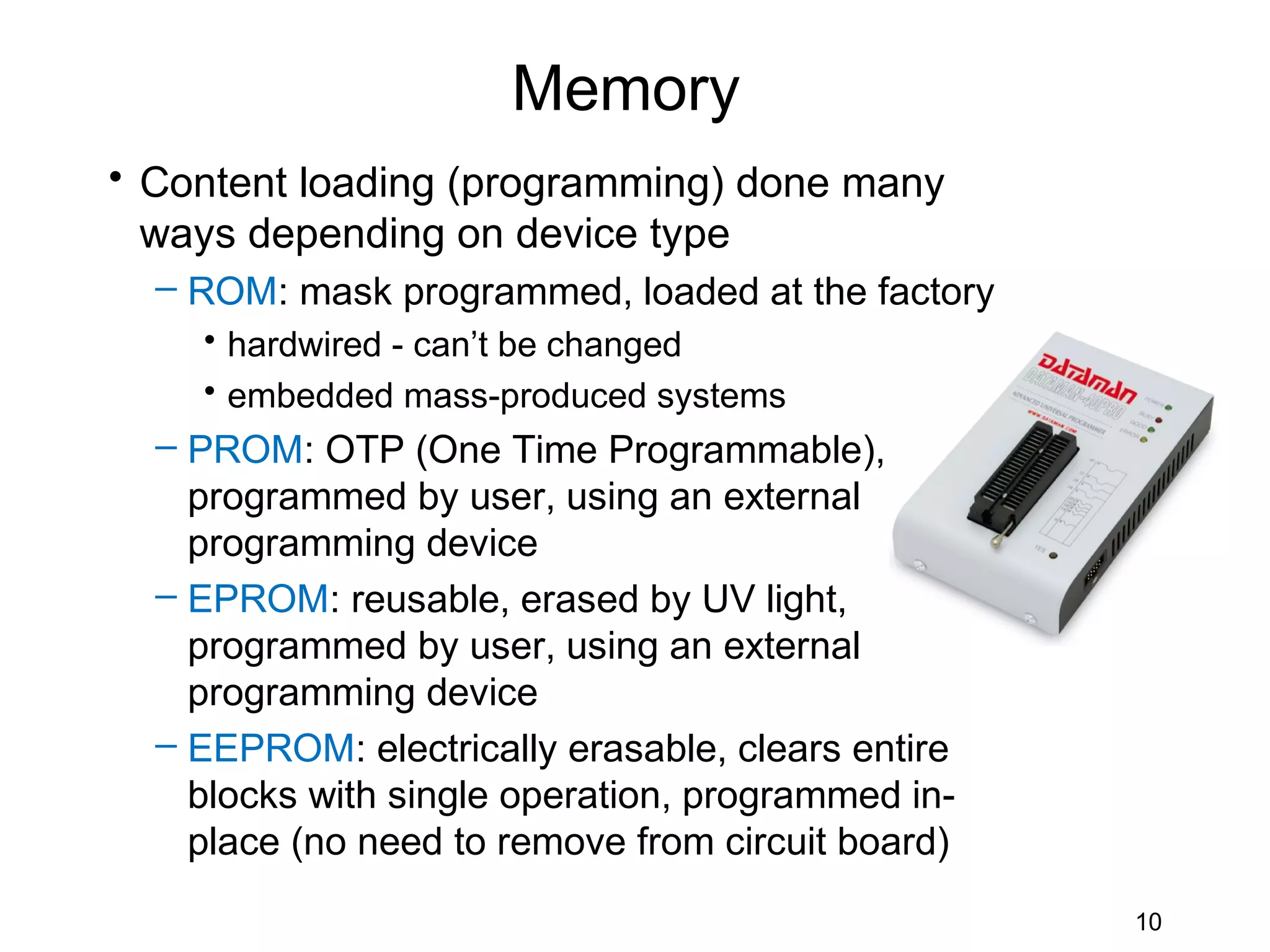
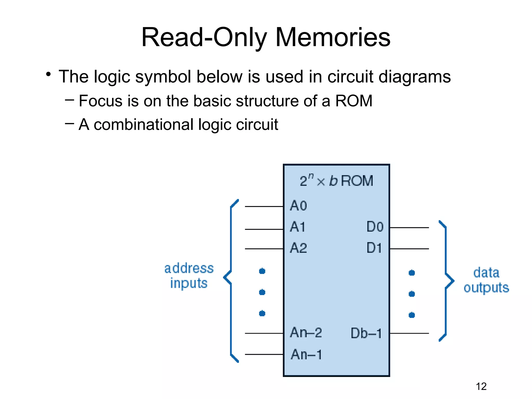
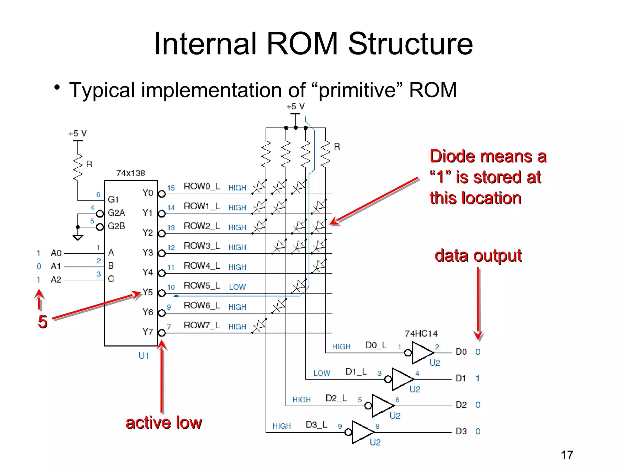
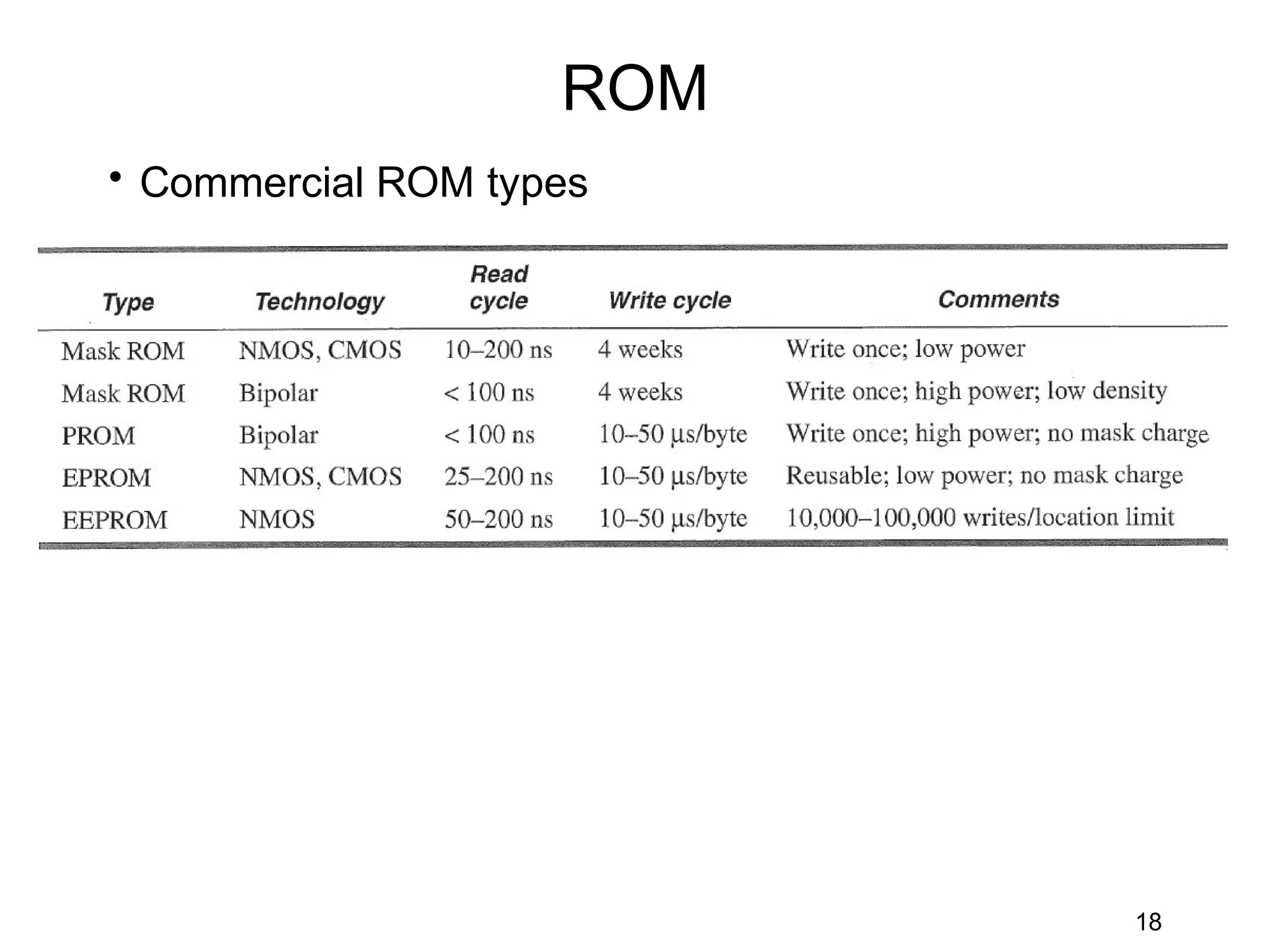
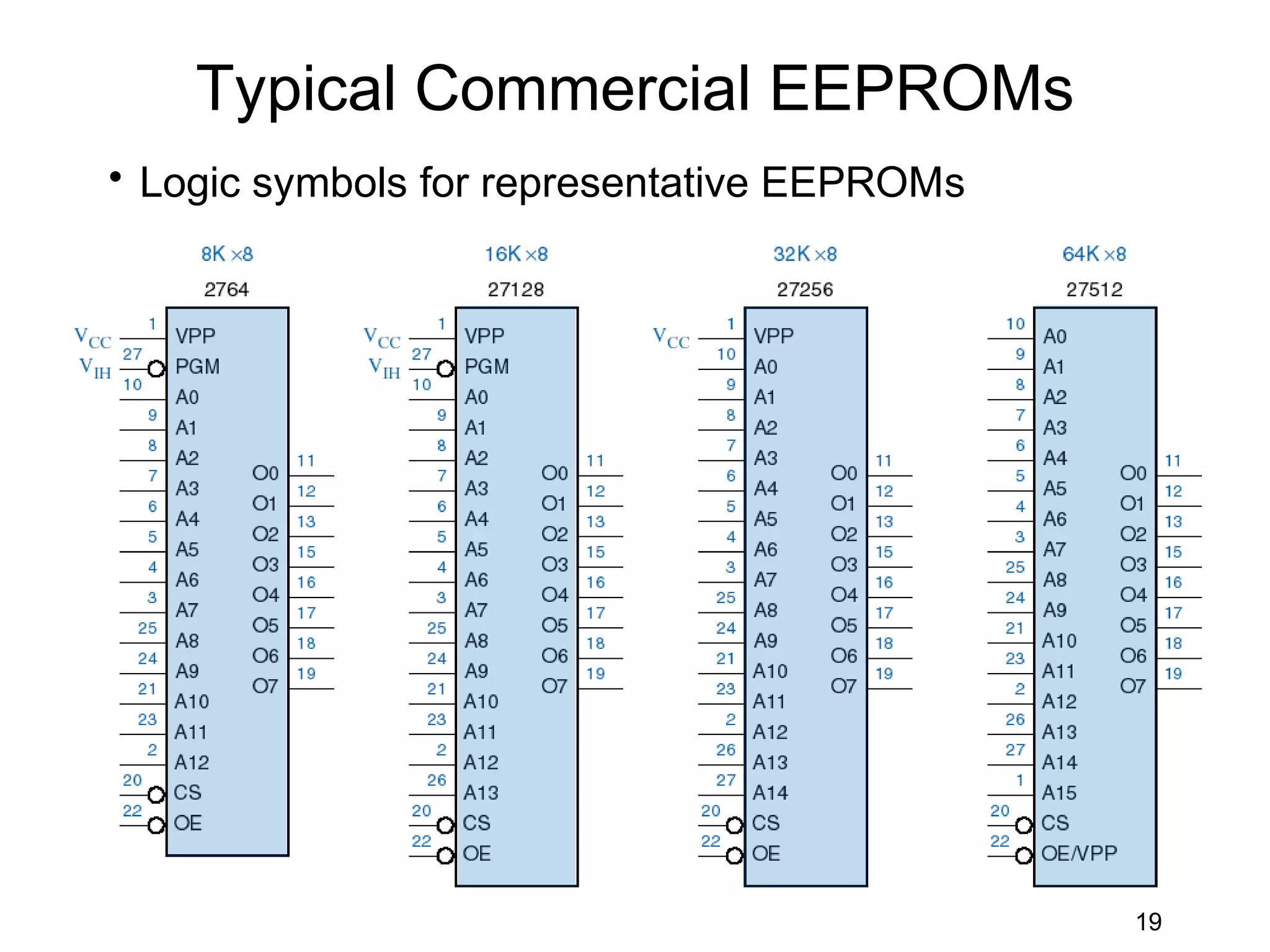
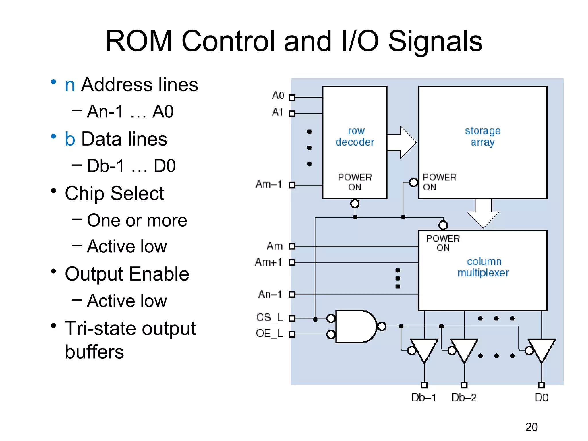
Overview of the internal structure of ROM, types of commercial ROM, and timing control signals.
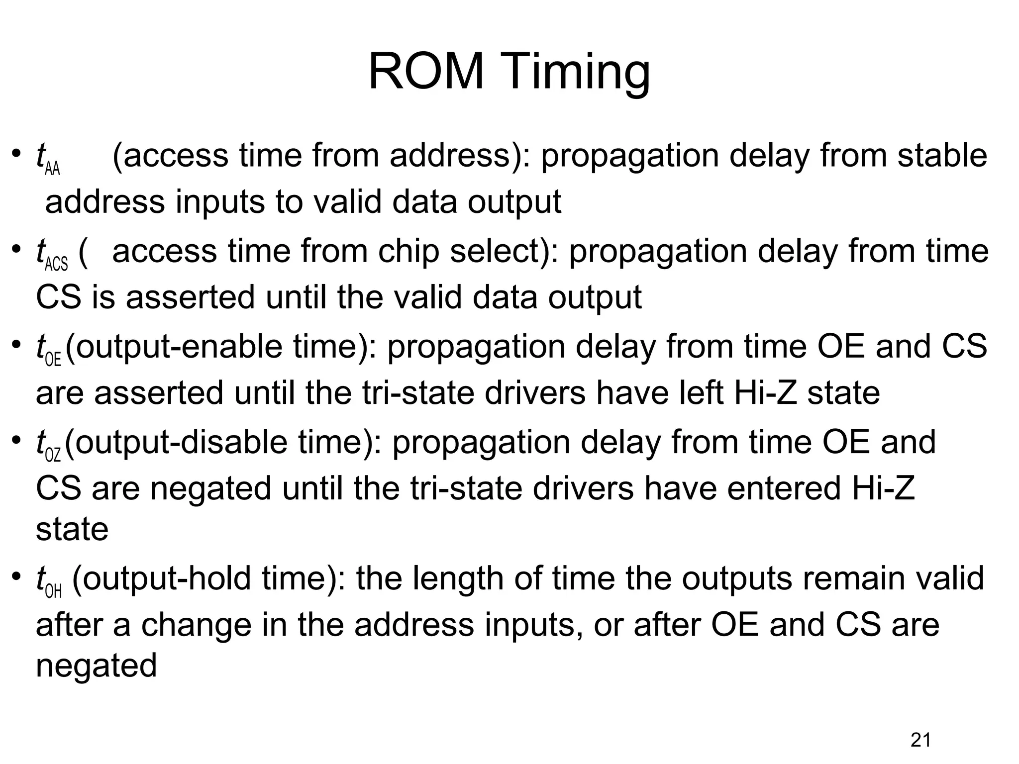
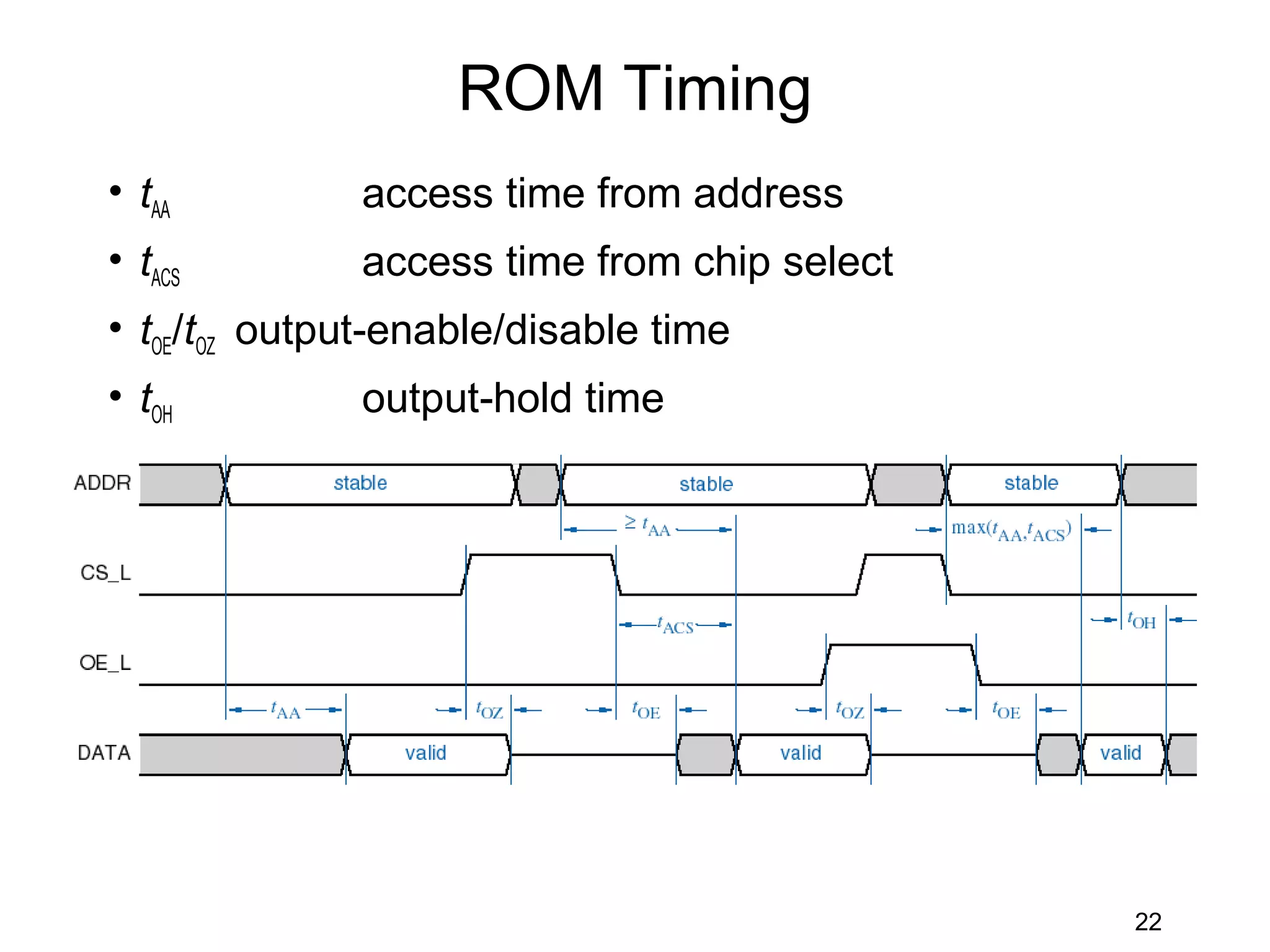
Details on ROM timing characteristics including access, output-enable and hold timings for effective operation.
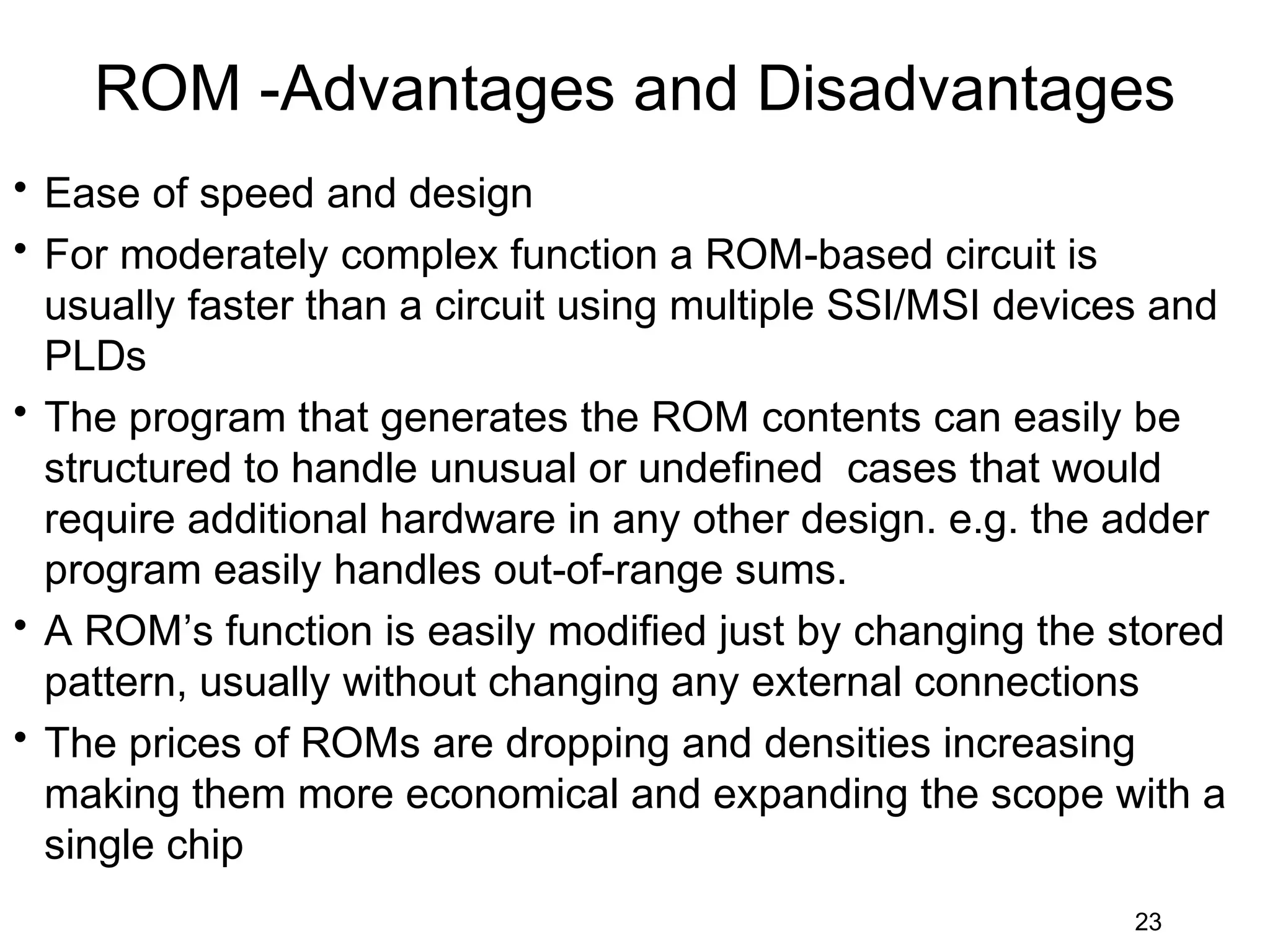
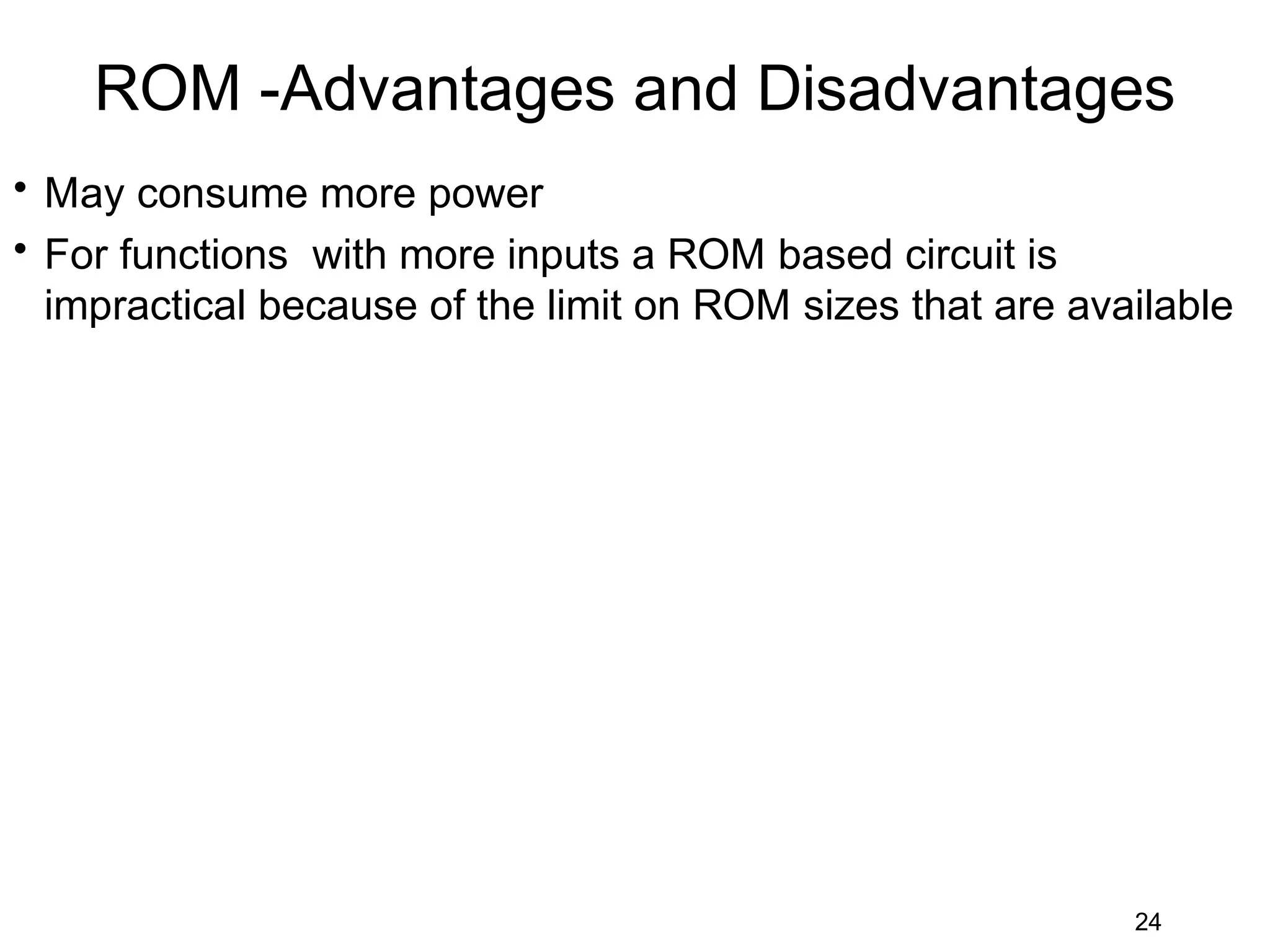
Outlines benefits of ROM in terms of speed and design, as well as limitations regarding power consumption and input complexity.