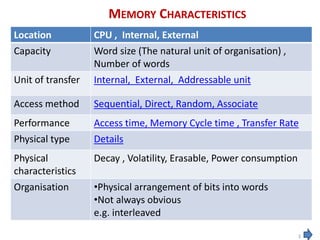
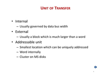
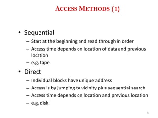
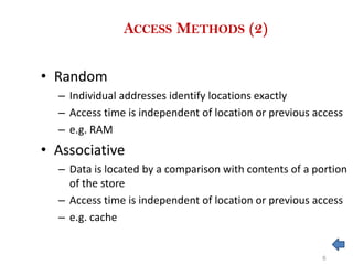
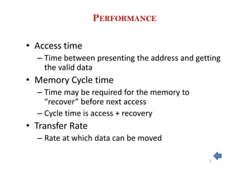
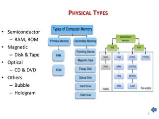
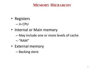
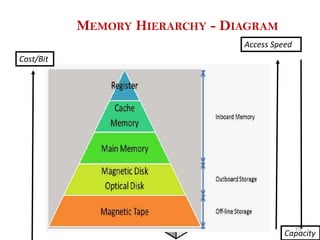
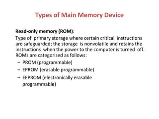
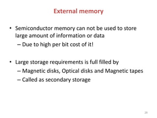
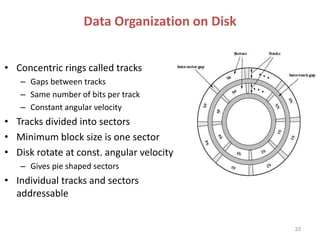
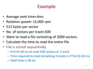
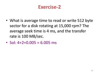
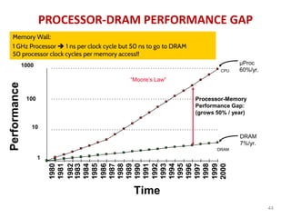
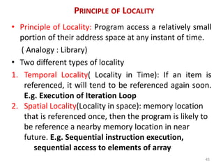
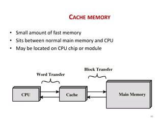
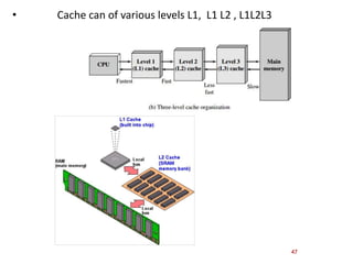
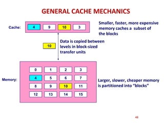
9953056974 Call Girls In South Ex, Escorts (Delhi) NCR.pdf
Unit IV Memory.pptx
1. Memory
Digital Electronics & Logic Design
Mr. M. V. Nimbalkar
Dept. of Computer Science & Engineering
MIT ADT’s School of Engineering, Loni, Pune
2. Introduction
Memory is a device that is used to store data or
programs on a temporary or permanent basis for use in
an electronic digital computer.
The memory is needed for the following purposes:
1. To store the program and data during execution
2. To store the program for repetitive use
3. To store the data for future or periodical use
4. To store the result of execution
3. MEMORY CHARACTERISTICS
3
Location CPU , Internal, External
Capacity Word size (The natural unit of organisation) ,
Number of words
Unit of transfer Internal, External, Addressable unit
Access method Sequential, Direct, Random, Associate
Performance Access time, Memory Cycle time , Transfer Rate
Physical type Details
Physical
characteristics
Decay , Volatility, Erasable, Power consumption
Organisation •Physical arrangement of bits into words
•Not always obvious
e.g. interleaved
4. UNIT OF TRANSFER
• Internal
– Usually governed by data bus width
• External
– Usually a block which is much larger than a word
• Addressable unit
– Smallest location which can be uniquely addressed
– Word internally
– Cluster on MS disks
4
5. ACCESS METHODS (1)
• Sequential
– Start at the beginning and read through in order
– Access time depends on location of data and previous
location
– e.g. tape
• Direct
– Individual blocks have unique address
– Access is by jumping to vicinity plus sequential search
– Access time depends on location and previous location
– e.g. disk
5
6. ACCESS METHODS (2)
• Random
– Individual addresses identify locations exactly
– Access time is independent of location or previous access
– e.g. RAM
• Associative
– Data is located by a comparison with contents of a portion
of the store
– Access time is independent of location or previous access
– e.g. cache
6
7. PERFORMANCE
• Access time
– Time between presenting the address and getting
the valid data
• Memory Cycle time
– Time may be required for the memory to
“recover” before next access
– Cycle time is access + recovery
• Transfer Rate
– Rate at which data can be moved
7
9. MEMORY HIERARCHY
• Registers
– In CPU
• Internal or Main memory
– May include one or more levels of cache
– “RAM”
• External memory
– Backing store
9
11. Types of main memory
Semiconductor Memory
Semiconductor memory uses semiconductor-based integrated
circuits to store information. Both volatile and non-volatile
forms of semiconductor memory exist.
Magnetic Memory
Magnetic storage uses different patterns of magnetization on a
magnetically coated surface to store information. Magnetic
storage is non-volatile.
13. Random access memory (RAM):
The part of primary storage that holds a software program
and small amounts of data when they are brought from
secondary storage. Rams are categorised as follows:
– SRAM (Static RAM) (flip-flop gates)
– DRAM (Dynamic RAM)
Types of Main Memory Device
14. Static RAM
• Memories that consists of circuits capable of retaining
their state as long as power is applied
• Bits stored as on/off switches
• Complex construction so larger per bit and more
expensive
14
15. SRAM Cell Organization
• Transistor arrangement gives
stable logic state
• State 1
– C1 high, C2 low, T1 T4 off, T2 T3 on
• State 0
– C2 high, C1 low, T2 T3 off, T1 T4 on
• Address line transistors are T5
and T6
15
16. Dynamic RAM
• Bits stored as charge in capacitors
charges leak so need refreshing
even when powered
• Simpler construction and smaller
per bit so less expensive
• Address line active when bit read or
written
– Transistor switch closed (current flows)
• Slower operations, used for main
memory
16
18. Difference
• Requires less memory. • Requires more memory.
• Access time is low. • Access time is more.
• Do not refresh.
• Faster access time.
• More power consumption.
• Needs to be refreshed.
• Slower access time.
• Less power consumption.
• Used in cache memory. • Used in main memory.
19. Block Diagram Of Ram
2k x nmemory
ADRS OUT
DATA
CS
WR
k
n
n
C S W R M e m o r y operation
0 x
1 0
1 1
N o n e
R e a d selected word
Write selected w o r d
20. Block Diagram Of Ram
This block diagram introduces the main interface to RAM.
A Chip Select, CS enables or disablesthe RAM.
ADRS specifies the address or location to read from
or write to.
WR selects between reading from or writing to the
memory.
Toread from memory, WR should be set to 0. OUT will be
the n-bit value stored atADRS.
Towrite to memory, we set WR = 1. DATAis the n-bit value
to save in memory.
21. MemorySizes
For example
A 224x 16RAM contains 224=16Mwords, each 16bitslong.
We refer to this as a 2kx nmemory.
There are k address lines, which can specify one of 2kaddresses.
Each address contains an n-bitword.
OUT
ADRS
DATA
CS
WR
k
n
n
2kx n memory
22. ReadingRAM
Toread from this RAM, the controlling circuit must:
Enable the chip by ensuring CS =1.
Select the read operation, by setting WR =0.
Send the desired address to the ADRSinput.
Tecontents of that address appear on OUT after a littlewhile.
Notice that the DATA input is unused for readoperations.
2kx n memory
OUT
ADRS
DATA
CS WR
k
n
n
23. WritingRAM
Towrite to this RAM, you need to:
Enable the chip by setting CS =1.
Select the write operation, by setting WR =1.
Send the desired address to the ADRSinput.
Send the word to store to the DATAinput.
The output OUT is not needed for memory writeoperations.
2k x n memory
OUT
ADRS
DATA
CS WR
k
n
n
24. Read-only memory (ROM):
Type of primary storage where certain critical instructions
are safeguarded; the storage is nonvolatile and retains the
instructions when the power to the computer is turned off.
ROMs are categorised as follows:
– PROM (programmable)
– EPROM (erasable programmable)
– EEPROM (electronically erasable
programmable)
Types of Main Memory Device
25. Read Only Memories
IF
E
Programmable read only memories (PROM) - are programmed
during manufacturing process. The contents of each memory cell is
locked by a fuse or antifuse (diodes). PROMs are used for
permanent data storage.
Erasable read only memories (EPROM) - there is a possibility to
erase EPROM with ultraviolet light (about 20 minutes) what sets all
bits in memory cells to 1. Programming requires higher voltage.
Memory cells are built with floating gate transistors. Data can be
stored in EPROMs for about 10 years.
Electrically erasable read only memories (EEPROM) - erasing does
not require ultraviolet light but higher voltage and can be applied
not to the whole circuit but to each memory cell separately.
26. N input bits
2Nwords by M bits
Implement M arbitrary functions of N variables
Example 8 words by 5 bits:
3 Input
Lines
A
B
C
F0 F1 F2 F3 F4
5 Output Lines
ROM
8 words
x 5 bits
Read Only Memory
27. .
.
n Inputs
Lines
m Outputs Lines
n bit
decoder
.
.
.
Memory Array
2n words x m bits
...
Read Only Memory – Internal Structure
28. External memory
• Semiconductor memory can not be used to store
large amount of information or data
– Due to high per bit cost of it!
• Large storage requirements is full filled by
– Magnetic disks, Optical disks and Magnetic tapes
– Called as secondary storage
28
29. Secondary Memory
Memory capacity that can store very large
amounts of data for extended periods of
time.
– It is nonvolatile.
– It takes much more time to retrieve data
because of the electromechanical nature.
– It is cheaper than primary storage.
– It can take place on a variety of media
30. Disk Connection to the System Bus
30
Processor Main Memory
Disk Controller
Disk Drive
System Bus
31. Magnetic Disk Structure
• Disk substrate (non magnetisable material) coated with
magnetisable material (e.g. iron oxide…rust)
• Advantage of glass substrate over aluminium
– Improved surface uniformity
– Reduction in surface defects
• Reduced read/write errors
– Lower fly heights
– Better stiffness
– Better shock/damage resistance
31
33. Data Organization on Disk
• Concentric rings called tracks
– Gaps between tracks
– Same number of bits per track
– Constant angular velocity
• Tracks divided into sectors
• Minimum block size is one sector
• Disk rotate at const. angular velocity
– Gives pie shaped sectors
• Individual tracks and sectors
addressable
33
34. Read and Write Mechanisms-1
• Recording & retrieval of data via conductive coil which
is called a head
• May be single read/write head or separate ones
• During read/write, head is stationary, platter rotates
• Write
– Electricity flowing through coil produces magnetic field
– Electric pulses sent to head
– Magnetic pattern recorded on surface below
34
35. Read and Write Mechanisms-2
• Read (traditional)
– Magnetic field moving relative to coil produces current
in coil
– Coil is the same for read and write (floppy disk)
• Read (contemporary)
– Separate read head, close to write head
– Partially shielded magneto resistive (MR) sensor
– Electrical resistance depends on direction of magnetic
field
– Resistance changes are detected as voltage signals
– Allows High frequency operation
• Higher storage density and speed
35
36. Disk Characteristics
• Fixed (rare) or movable head
– Fixed head
• One read/write head per track mounted on fixed ridged arm
– Movable head
• One read/write head per side mounted on a movable arm
• Removable or fixed disk
• Single or double (usually) sided
• Head mechanism
– Contact (Floppy), Fixed gap, Flying (Winchester)
• Single or multiple platter
36
38. Capacity
• Vendors express capacity in units of gigabytes (GB),
where 1 GB =10^9 Byte
• Capacity is determined by these technology factors:
– Recording density (bits/in): number of bits that can be
squeezed into a 1 inch segment of a track.
– Track density (tracks/in): number of tracks that can be
squeezed into a 1 inch radial segment.
– Areal density (bits/in2): product of recording and track
density.
• Modern disks partition tracks into disjoint
subsets called recording zones
38
39. Computing Disk Capacity
• Capacity =(# bytes/sector) x (avg. # sectors/track) x
(# tracks/surface) x (# surfaces/platter) x
(# platters/disk)
• Example:
– 512 bytes/sector, 300 sectors/track (average)
– 20,000 tracks/surface, 2 surfaces/platter
– 5 platters/disk
– Capacity = 512 x 300 x 20000 x 2 x 5 = 30.72GB
39
40. Disk Performance Parameters
• Seek time (Ts)
– Time require to positioned the head on the desired track
• Rotational delay
– Time require to positioned desired sector under r/w head
• Transfer time
• The total average access time is:
Ta = Ts+ 1/2r + b/rN
– Here Ts is Average seek time
– r is rotation speed in revolution per second
– b number of bytes to be transferred
– N number of bytes on a track
40
41. Example
• Average seek time=4ms
• Rotation speed= 15,000 rpm
• 512 bytes per sector
• No. of sectors per track=500
• Want to read a file consisting of 2000 sectors.
• Calculate the time to read the entire file
• File is stored sequentially.
– 4+2+4=10 ms to read 500 sectors or 1 track
– Time required to read remaining 4 tracks is 3*(4+2)=18 ms
– Total time is 28 ms
41
42. Exercise-2
• What is average time to read or write 512 byte
sector for a disk rotating at 15,000 rpm? The
average seek time is 4 ms, and the transfer
rate is 100 MB/sec.
• Sol: 4+2+0.005 = 6.005 ms
42
43. 43
DRAM CAPACITY GROWTH
• 4X capacity increase almost every 3 years, i.e., 60% increase
per year for 20 years
• Unprecedented growth in density, but we still have a
problem
45. PRINCIPLE OF LOCALITY
• Principle of Locality: Program access a relatively small
portion of their address space at any instant of time.
( Analogy : Library)
• Two different types of locality
1. Temporal Locality( Locality in Time): If an item is
referenced, it will tend to be referenced again soon.
E.g. Execution of Iteration Loop
2. Spatial Locality(Locality in space): memory location
that is referenced once, then the program is likely to
be reference a nearby memory location in near
future. E.g. Sequential instruction execution,
sequential access to elements of array
45
46. CACHE MEMORY
• Small amount of fast memory
• Sits between normal main memory and CPU
• May be located on CPU chip or module
46
47. • Cache can of various levels L1, L1 L2 , L1L2L3
47
48. GENERAL CACHE MECHANICS
48
0 1 2 3
4 5 6 7
8 9 10 11
12 13 14 15
Larger, slower, cheaper memory
is partitioned into “blocks”
Data is copied between
levels in block-sized
transfer units
8 9 14 3
Smaller, faster, more expensive
memory caches a subset of
the blocks
Cache:
Memory: 4
4
4 10
10
10