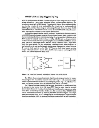
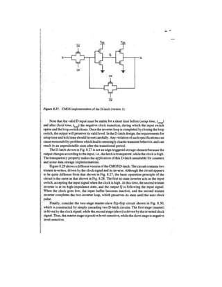
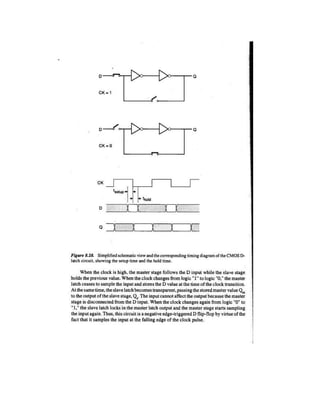
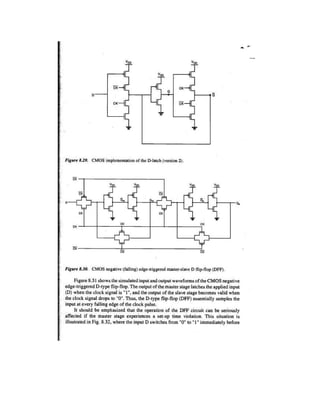
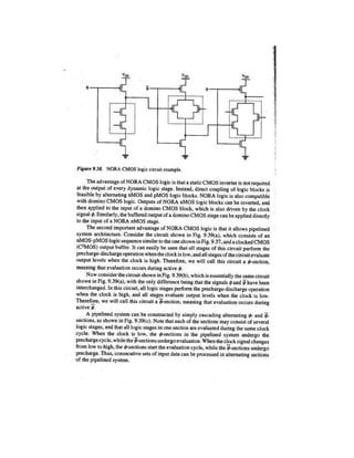
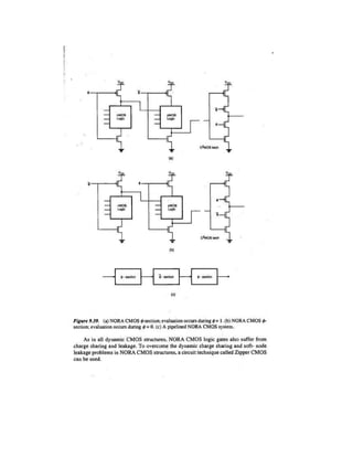
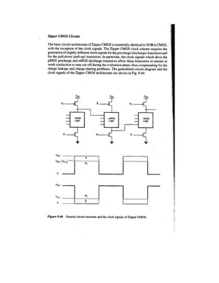
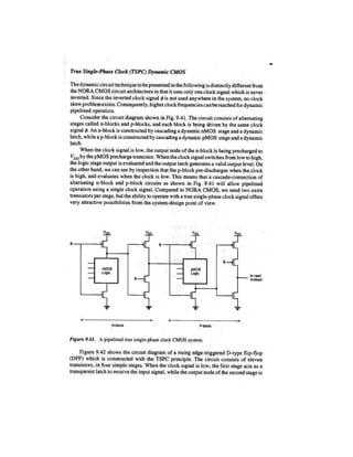
CMOS DIGITAL IC DESIGN
Lecture Notes
M. TECH (VLSI & ES)
(I YEAR I SEM)
(2022-2023)
Prepared by
Dr. Amairullah Khan Lodhi
Director R & D, Professor
SHADAN COLLEGE OF ENGINEERING & TECHNOLOGY
Peerancheru, Hyderabad-500086
Department of Electronics and Communication Engineering
Recognized under 2(f) and 12 (B) of UGC ACT 1956
(Affiliated to JNTUH, Hyderabad, Approved by AICTE-Accredited by NBA & NAAC-A+ Grade
ELECTIVE-II
CMOS DIGITAL IC DESIGN
Course Objectives:
To discuss basic CMOS logic gates, implementation of AOI and OAI gates
Design MOS logic circuits using Transmission gates
To analyze different delays and power dissipation in number of stages.
To understand the design of combinational circuits using ratioed, cascade and dynamic logic.
To design different types of Semiconductor Memories
UNIT I:
MOS Design:
Pseudo NMOS Logic Inverter, Inverter threshold voltage, Output high voltage, Output Low voltage,
Gain at gate threshold voltage, Transient response, Rise time, Fall time, Pseudo NMOS logic gates,
Transistor equivalency, CMOS Inverter logic.
UNIT II:
Combinational MOS Logic Circuits:
MOS logic circuits with NMOS loads, Primitive CMOS logic gates NOR & NAND gate, Complex Logic
circuits design Realizing Boolean expressions using NMOS gates and CMOS gates , AOI and OIA
gates, CMOS full adder, CMOS transmission gates, Designing with Transmission gates.
UNIT III:
Sequential MOS Logic Circuits:
Behavior of Bi-stable elements, SR Latch, Clocked latch and flip flop circuits, CMOS D latch and edge
triggered Flip-flop.
UNIT IV:
Dynamic Logic Circuits:
Basic principle, Voltage Bootstrapping, Synchronous dynamic pass transistor circuits, Dynamic CMOST
Transmission gate logic, High performance Dynamic CMOS circuits.
UNIT V:
Semiconductor Memories:
Types, RAM array organization, DRAM Types, Operation, Leakage currents in DRAM cell and refresh
operation, SRAM operation Leakage currents in SRAM cells, Flash Memory- NOR flash and NAND
flash.
TEXT BOOKS:
1. Digital Integrated Circuit Design Ken Martin, Oxford University Press, 2011.
2. CMOS Digital Integrated Circuits Analysis and Design Sung-Mo Kang, Yusuf Leblebici,
TMH, 3 rd Ed., 2011.
REFERENCE BOOKS:
1. Introduction to VLSI Systems: A Logic, Circuit and System Perspective Ming-BO Lin, CRC
Press, 2011
2. Digital Integrated Circuits A Design Perspective, Jan M. Rabaey, Anantha Chandrakasan,
Borivoje Nikolic, 2 nd Ed., PHI.
Course Outcomes:
Able to apply mathematical methods and transistor physics in the analysis of CMOS circuits
and design CMOS inverter with different loads for given levels noise margins and propagation
Can execute moderately sized digital logic designs with OAI, AOI, and transmission gates.
Able to design static and dynamic CMOS circuits (both Combinational and sequential) at
transistor level and layout level.
Able to design memory architectures that aids the growth of VLSI designs with reduced access
time and reduced power consumption.
CMOS-IC Design NOTES Lodhi.pdf

CMOS-IC Design NOTES Lodhi.pdf

  • 1.
    CMOS DIGITAL ICDESIGN Lecture Notes M. TECH (VLSI & ES) (I YEAR I SEM) (2022-2023) Prepared by Dr. Amairullah Khan Lodhi Director R & D, Professor SHADAN COLLEGE OF ENGINEERING & TECHNOLOGY Peerancheru, Hyderabad-500086 Department of Electronics and Communication Engineering Recognized under 2(f) and 12 (B) of UGC ACT 1956 (Affiliated to JNTUH, Hyderabad, Approved by AICTE-Accredited by NBA & NAAC-A+ Grade
  • 2.
    ELECTIVE-II CMOS DIGITAL ICDESIGN Course Objectives: To discuss basic CMOS logic gates, implementation of AOI and OAI gates Design MOS logic circuits using Transmission gates To analyze different delays and power dissipation in number of stages. To understand the design of combinational circuits using ratioed, cascade and dynamic logic. To design different types of Semiconductor Memories UNIT I: MOS Design: Pseudo NMOS Logic Inverter, Inverter threshold voltage, Output high voltage, Output Low voltage, Gain at gate threshold voltage, Transient response, Rise time, Fall time, Pseudo NMOS logic gates, Transistor equivalency, CMOS Inverter logic. UNIT II: Combinational MOS Logic Circuits: MOS logic circuits with NMOS loads, Primitive CMOS logic gates NOR & NAND gate, Complex Logic circuits design Realizing Boolean expressions using NMOS gates and CMOS gates , AOI and OIA gates, CMOS full adder, CMOS transmission gates, Designing with Transmission gates. UNIT III: Sequential MOS Logic Circuits: Behavior of Bi-stable elements, SR Latch, Clocked latch and flip flop circuits, CMOS D latch and edge triggered Flip-flop. UNIT IV: Dynamic Logic Circuits: Basic principle, Voltage Bootstrapping, Synchronous dynamic pass transistor circuits, Dynamic CMOST Transmission gate logic, High performance Dynamic CMOS circuits. UNIT V: Semiconductor Memories: Types, RAM array organization, DRAM Types, Operation, Leakage currents in DRAM cell and refresh operation, SRAM operation Leakage currents in SRAM cells, Flash Memory- NOR flash and NAND flash.
  • 3.
    TEXT BOOKS: 1. DigitalIntegrated Circuit Design Ken Martin, Oxford University Press, 2011. 2. CMOS Digital Integrated Circuits Analysis and Design Sung-Mo Kang, Yusuf Leblebici, TMH, 3 rd Ed., 2011. REFERENCE BOOKS: 1. Introduction to VLSI Systems: A Logic, Circuit and System Perspective Ming-BO Lin, CRC Press, 2011 2. Digital Integrated Circuits A Design Perspective, Jan M. Rabaey, Anantha Chandrakasan, Borivoje Nikolic, 2 nd Ed., PHI. Course Outcomes: Able to apply mathematical methods and transistor physics in the analysis of CMOS circuits and design CMOS inverter with different loads for given levels noise margins and propagation Can execute moderately sized digital logic designs with OAI, AOI, and transmission gates. Able to design static and dynamic CMOS circuits (both Combinational and sequential) at transistor level and layout level. Able to design memory architectures that aids the growth of VLSI designs with reduced access time and reduced power consumption.