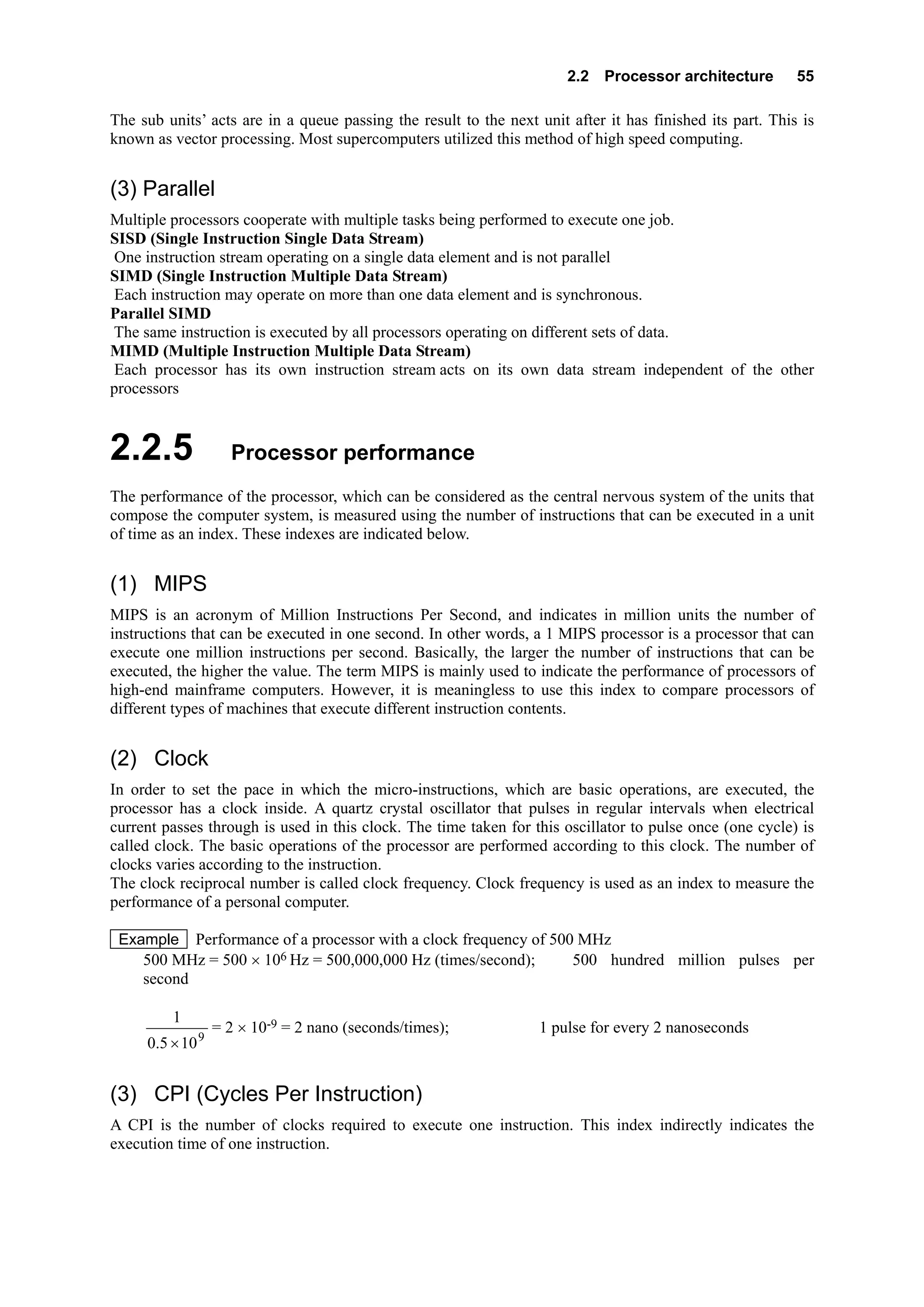
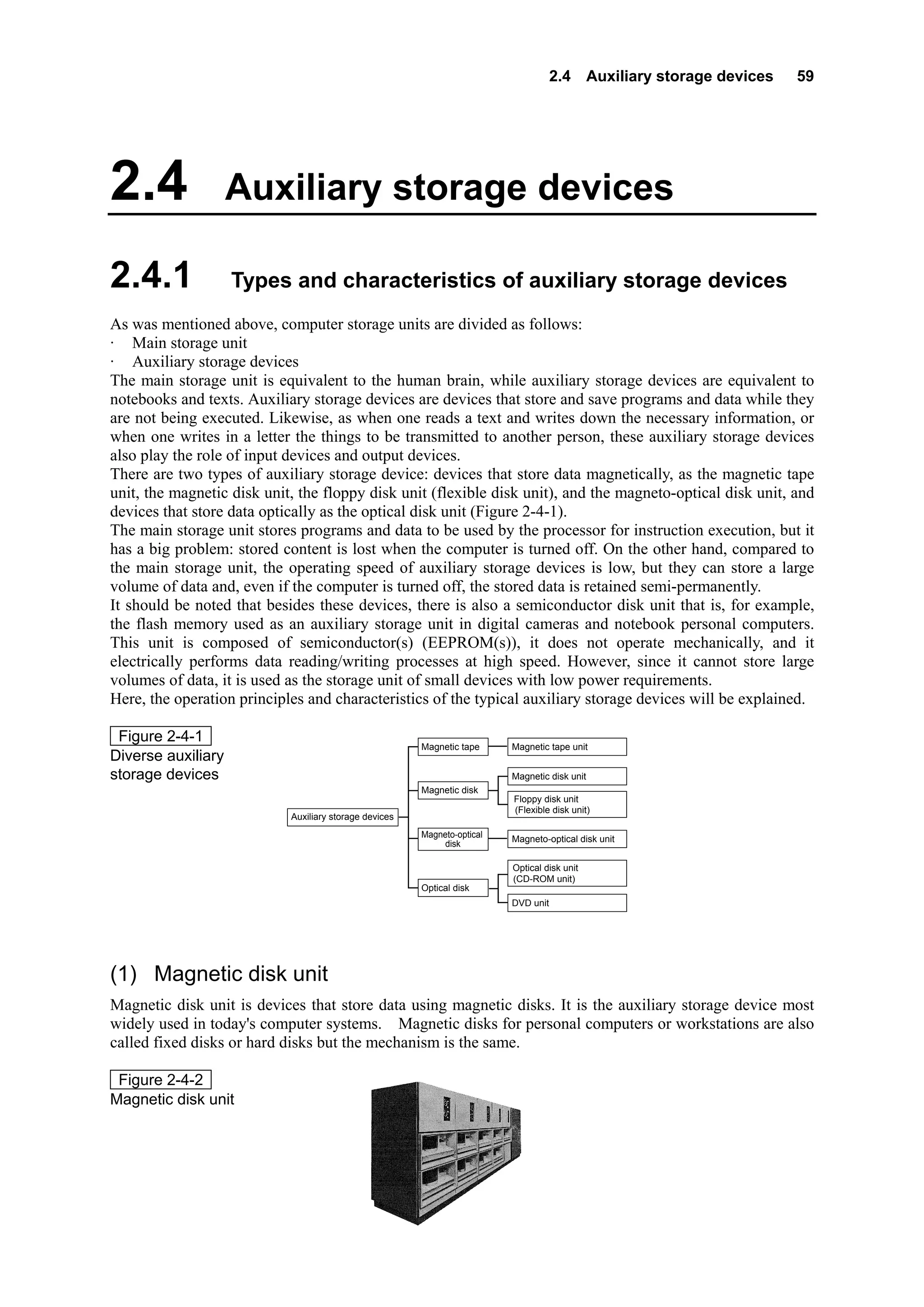
The document discusses the five main units of computer hardware: input, storage, operation, control, and output. It describes each unit's function and role, which is analogous to parts of the human body. The storage unit is divided into main storage and auxiliary storage. The document also provides details on integrated circuits, semiconductor memory including RAM and ROM, and different types of RAM and ROM.


![2.3 Memory architecture 57
turned off, the contents stored are not lost, they can be used as input/output units of large volumes of data.
· The following are the main auxiliary storage devices.
· Magnetic tape unit
· Magnetic disk unit
· Floppy disk unit (Flexible disk unit)
· Optical disk unit
· Magneto-optical disk unit
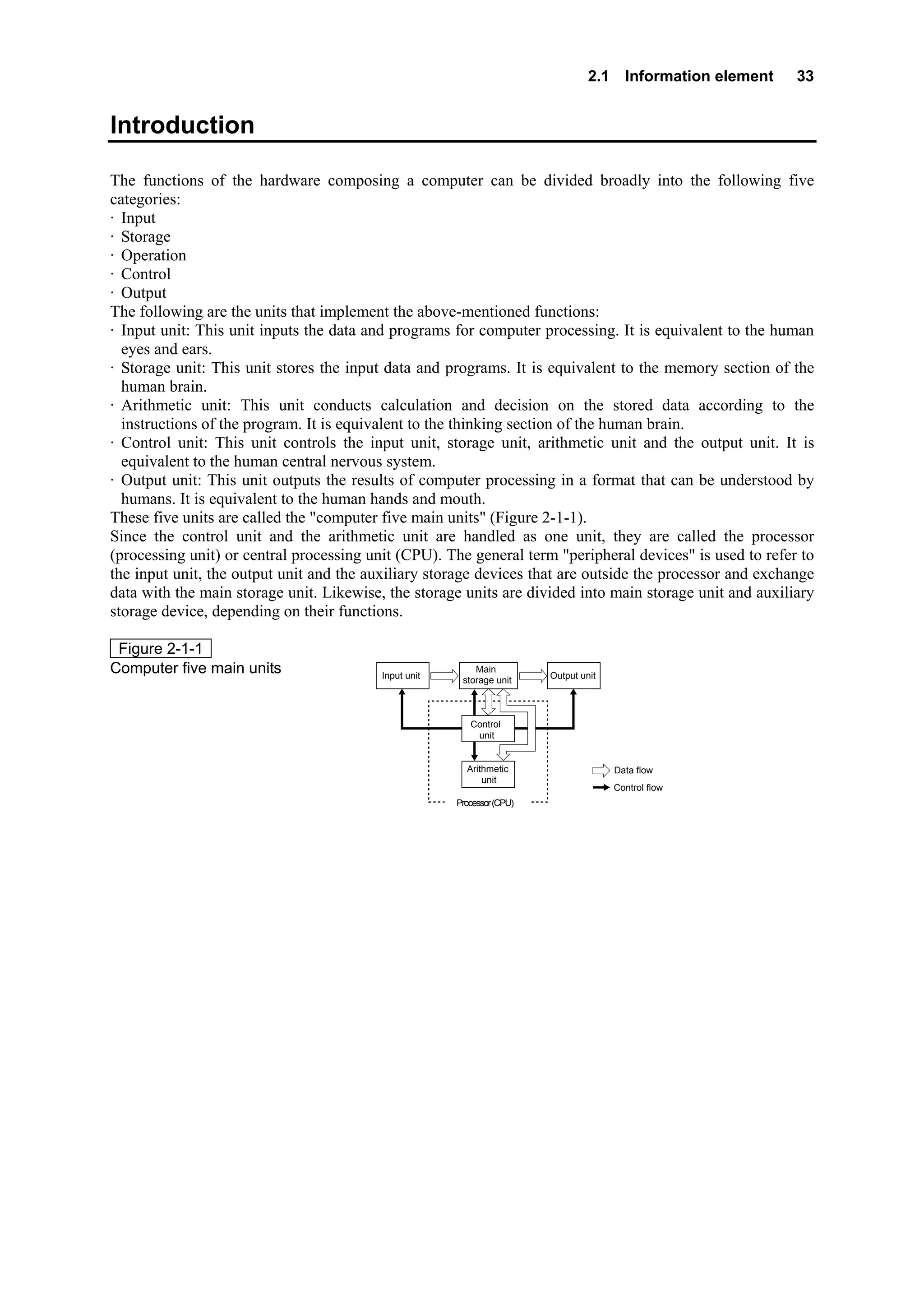
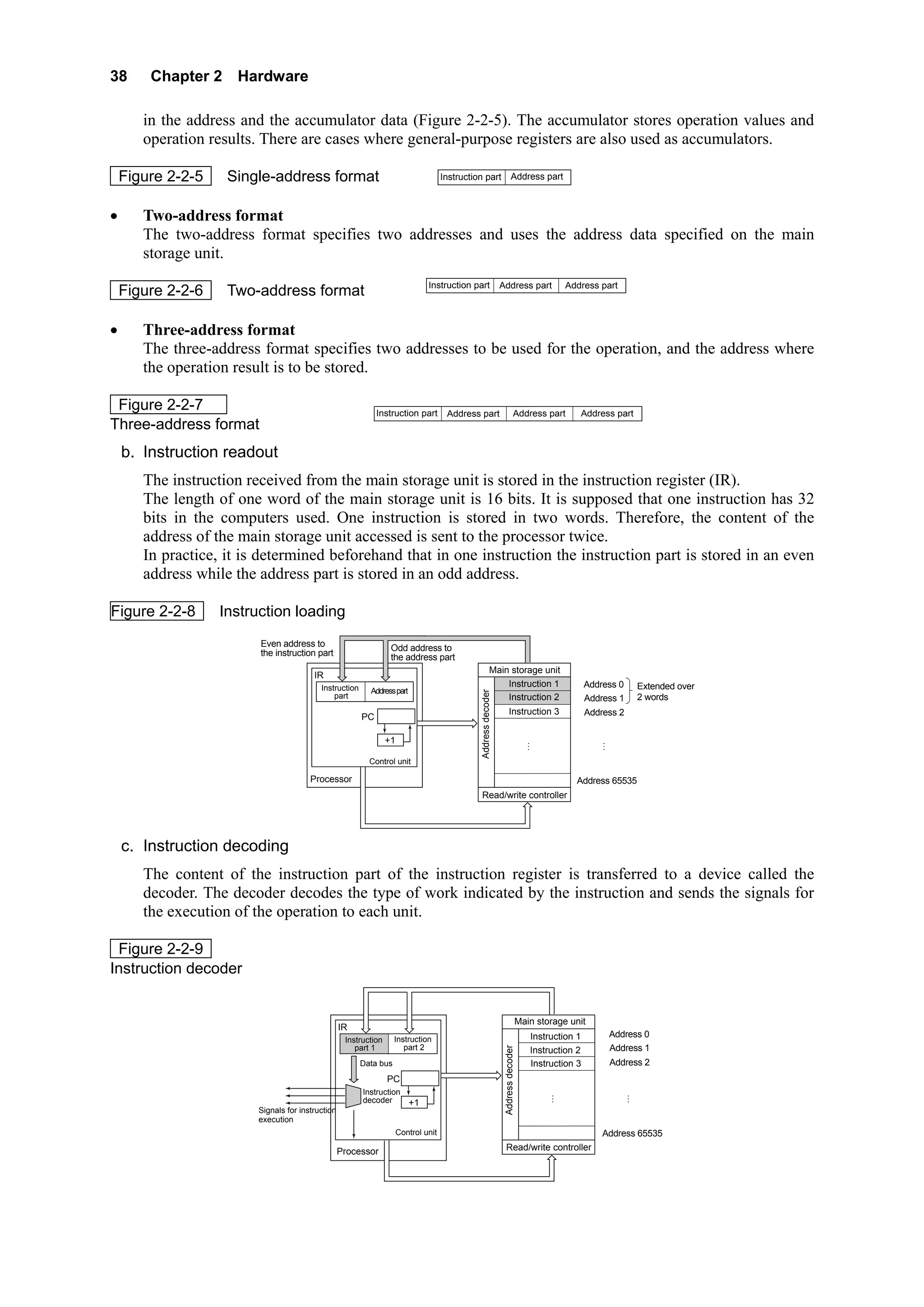
2.3.2 Memory capacity and performance
(1) Memory hierarchical structure
The computer memory is composed of the register inside the processor, the main storage unit, the auxiliary
storage devices, etc. The storage capacity and the processing speed of each of these devices differ. As is
shown in Figure 2-3-3, the access speed is as follows:
(High speed) Register inside the processor > Main storage unit > Auxiliary storage devices (Low speed)
This access speed difference is absorbed by a device called the buffer.
Figure 2-3-3 Memory hierarchical structure
[Access speed] [Storage capacity]
1 to 10 nanoseconds Register 100 bytes
1 to 100 nanoseconds Cache memory 100 k bytes
Hundreds of nanoseconds Main storage unit 10 to 100M bytes
100 microseconds 100M bytes
Disk cache
to 10 milliseconds to 1G byte
Hundreds of milliseconds Magnetic disk unit, magnetic tape unit, Over tens of M bytes
to hundreds of seconds optical disk unit, magneto-optical disk unit, etc. to 100G bytes
(2) Access time
The access time and cycle time indicate the operation speed of the storage units.
The access time is the time elapsed from when the processor sends the read/write instruction to the storage
unit until the data delivery/acceptance is completed.
For the processor to access the main storage unit data, the following three stages are necessary:
The time during which the processor requests the data readout
The time during which the processor selects the main storage unit address with the address bus
The time during which the data of the selected address is transferred through the data bus.
In other words, + + represent the time elapsed from when the data access request is sent until the data
transfer is completed. This lapse of time is called the access time.
(3) Cycle time
Among the storage elements of the storage unit, when data is to be stored in the capacitor, there are some
whose memory fades with time, as the DRAM. In this case, the refreshing operation that rewrites data at
regular intervals becomes necessary. For that reason, after the data transfer is completed, a preparation time
in order to receive the next request becomes necessary. The lapse of time that includes the point up to this
preparation is called cycle time.](https://image.slidesharecdn.com/no-1part1chap2-120309003504-phpapp02/75/Processor-architecture-26-2048.jpg)
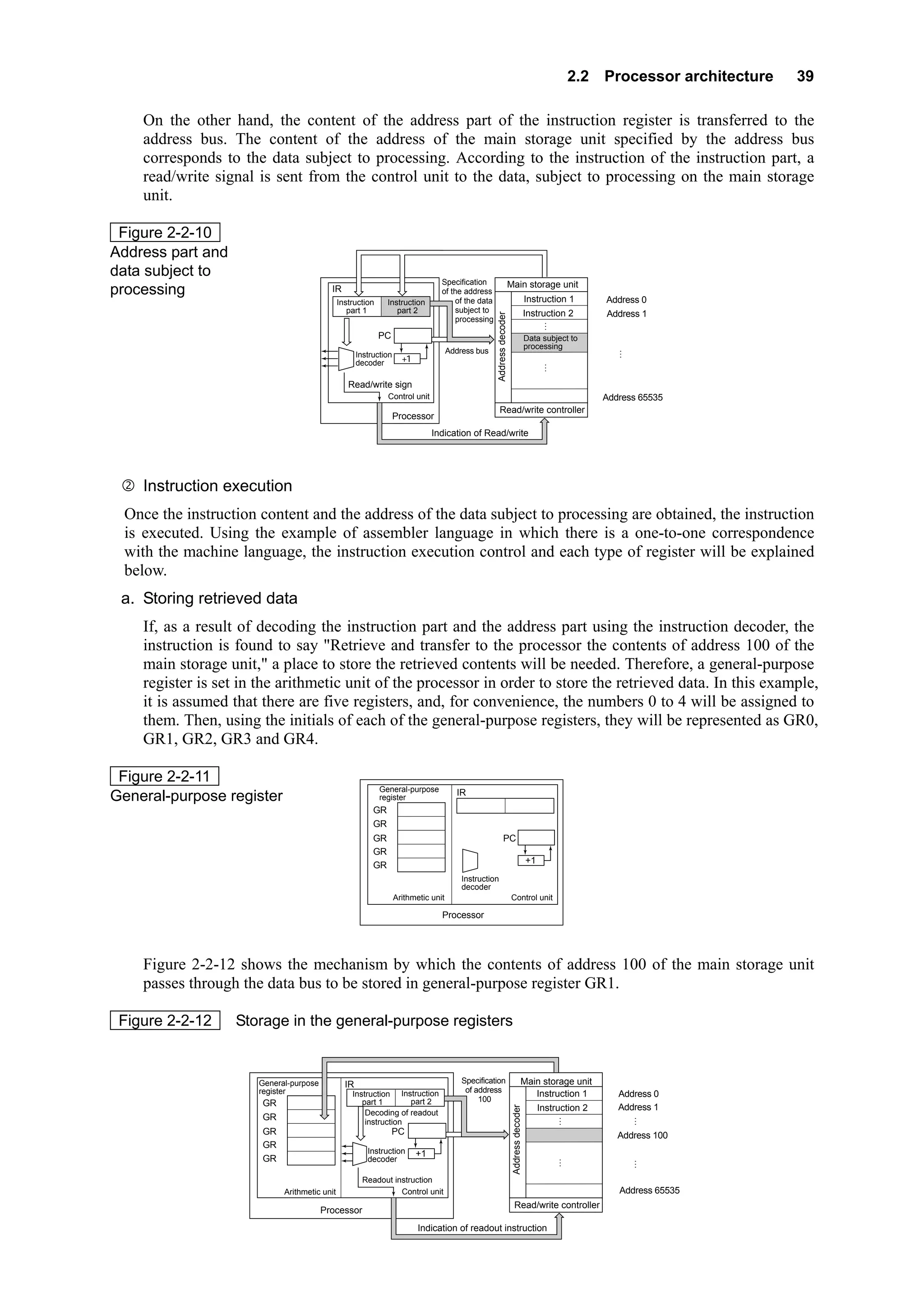
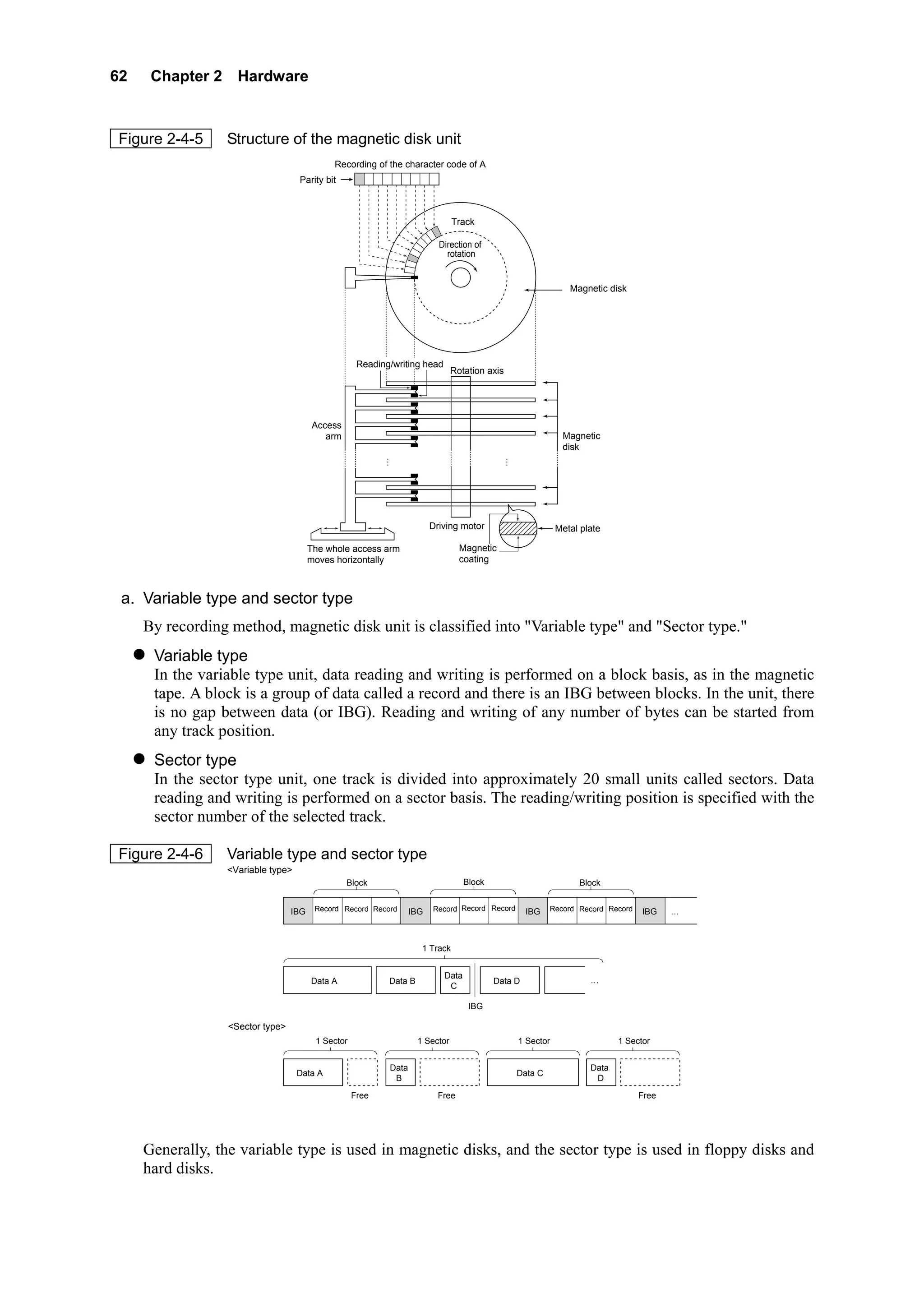
![60 Chapter 2 Hardware
Magnetic disk
a. Track
The magnetic disk is a circle-shaped magnetic body in which data is recorded along rings called tracks.
There are several tracks concentrically set on the magnetic disk. The length of the outer tracks and that
of the inner tracks differ, because of the difference of the storage capacity, the volume of data stored is
the same in every track. (Figure 2-4-3).
Outer side track
Figure 2-4-3 Inner side track
Same storage capacity
Data recording side
of the magnetic disk
Storage density: High
Storage density: Low
The storage density of the disk is based on the average track length and the storage capacity of the
magnetic disk is determined by the number of tracks and the storage density of one disk.
b. Cylinder
In a magnetic disk unit, which is composed of multiple magnetic disks, the group of tracks with the
same radius on each of the disks is set as one data storage area. This storage area is called a cylinder.
When data is stored in a cylinder, if, for example, the data cannot be completely stored on track 0 of
cylinder 1, it can be stored on track 1, track 2, etc. of the same cylinder. Therefore, since data access
can be performed without moving the access arm (that is, the magnetic head), it is extremely efficient.
To put it in another way, the cylinder is a group of tracks that can be read and written by multiple
magnetic heads if the access arm of the magnetic disk unit is fixed.
Figure 2-4-4 Cylinder 2
Tracks and cylinders Cylinder 1
Cylinder 0
Tracks
0
1
2
⋮
⋮
c. Storage capacity
The storage capacity of the magnetic disk can be determined as follows:
Storage capacity of 1 track × Track number of 1 cylinder × Cylinder number of the magnetic disk
Example
Given a magnetic disk with the following specifications, the storage capacity of this magnetic disk
is calculated:
[Magnetic disk specifications]
• Cylinder number: 800 cylinders
• Track number/cylinder number: 19 tracks
• Storage capacity/track: 20,000 bytes
The storage capacity per cylinder is as follows:
20,000 bytes/track × 19 tracks/cylinder = 380,000 bytes/cylinder = 380 kB (kilo bytes)
Since the number of cylinders on this disk is 800, the storage capacity of the magnetic disk is as
follows:](https://image.slidesharecdn.com/no-1part1chap2-120309003504-phpapp02/75/Processor-architecture-29-2048.jpg)
![2.4 Auxiliary storage devices 61
380 kB/cylinder × 800 cylinders = 304,000 kB = 304 MB (Mega bytes)
An example of the calculation of storage capacity when blocking is performed is shown below.
Example
Given a magnetic disk with the following specifications, the number of cylinders required when 80
thousand records of 200 bytes each are stored in a sequential access file of 10 records/block per
magnetic disk is calculated. It should be noted that block recording cannot be extended over
multiple tracks.
[Magnetic disk specifications]
• Cylinder number: 400 cylinders
• Track number/cylinder number: 19 tracks
• Storage capacity/tracks: 20,000 bytes
• Inter-block gap (IBG): 120 bytes
1. First, the number of blocks of the whole file is calculated.
Since the number of records is 80,000 and the blocking factor is 10, the number of blocks is
determined as follows:
80,000 records ÷ 10 records/block = 8,000 blocks
2. The length of 1 block, including the inter-block gap is calculated.
200 bytes/record × 10 records/block + 120 bytes/block = 2,120 bytes/block
3. The number of blocks that can be recorded in 1 track is calculated.
20,000 bytes/track ÷ 2,120 bytes/block = 9.43… blocks/track
Since a block cannot be recorded across multiple tracks, the decimals are omitted, and the
number of blocks that can be recorded in 1 track becomes 9 blocks/track.
4. The number of tracks required for the whole file is calculated.
8,000 blocks ÷ 9 blocks/track =888.88… tracks
Rounding it up to the next whole number, it becomes 889 tracks.
5. The number of cylinders required to record the whole file is
889 tracks ÷ 19 tracks/cylinder = 46.78…cylinders
Rounding it up to the next whole number, it becomes 47 cylinders.
Magnetic disk unit structure and operation principles
The magnetic disk unit has multiple magnetic disks, which it rotates at high speeds in order to record data
along concentric tracks. On each recording side, an access arm with a magnetic head moves forward and
backward to reach the track position where data is to be read or recorded.
Compared to the sequential access of the magnetic tape unit, in which access can only be performed in
order from the beginning, in the magnetic disk unit, besides sequential access, direct access to the desired
recording position can also be performed. Auxiliary storage devices in which this direct access can be
performed are called direct access storage devices (DASD).](https://image.slidesharecdn.com/no-1part1chap2-120309003504-phpapp02/75/Processor-architecture-30-2048.jpg)
![64 Chapter 2 Hardware
Data transfer time
The time elapsed between when the magnetic head data access starts and when the transfer is
completed is called data transfer time.
Therefore, the time elapsed between when the magnetic disk unit starts the data access and when the data
transfer is completed, that is, the access time, is calculated as follows:
Seek time + Search time + Data transfer time
Strictly speaking, as in the above-mentioned formula, the time elapsed between when the access request
occurs and the magnetic disk unit starts operating is the access time.
Access time of the magnetic disk unit = Average seek time + Average search time +
Data transfer time
Example
Given a magnetic disk unit with the following specifications, the access time of this magnetic disk
when a record of 9,000 bytes is processed is calculated.
[Magnetic disk unit specifications]
· Capacity per track: 15,000 bytes
· Magnetic disk rotation speed: 3,000 revolutions/minute
· Average seek time: 20 milliseconds
1. First, the average search time is calculated.
Since the rotation speed of the magnetic disk is 3,000 revolutions/minute, through the following
operation,
3,000 revolutions/minute ÷ 60 seconds/minute = 50 revolutions/second,
it is determined that the magnetic disk makes 50 revolutions per second. Therefore, the time
required to make 1 revolution is as follows:
1 revolution ÷ 50 revolutions/second = 0.02 seconds/revolution = 20 milliseconds
Since the average search time is the time required to make 1/2 revolution, it is as follows:
20 milliseconds ÷ 2 = 10 milliseconds
2. Since in 1 revolution, the information contained in 1 track passes through the magnetic head,
considering that the disk makes 50 revolutions per second, the data transfer speed is as follows:
Data transfer speed = 50 tracks/second × 15,000 bytes/track = 750 × 103 bytes/second
Based on this data transfer speed, the time to transfer 9,000 bytes of data can be calculated as
follows.
(9 × 103 bytes) ÷ (750 × 103 bytes/second) = 0.012 seconds = 12 milliseconds
3. Therefore, the access time is as follows:
Average seek time + Average search time + Data transfer time
= 20 milliseconds + 10 milliseconds + 12 milliseconds = 42 milliseconds
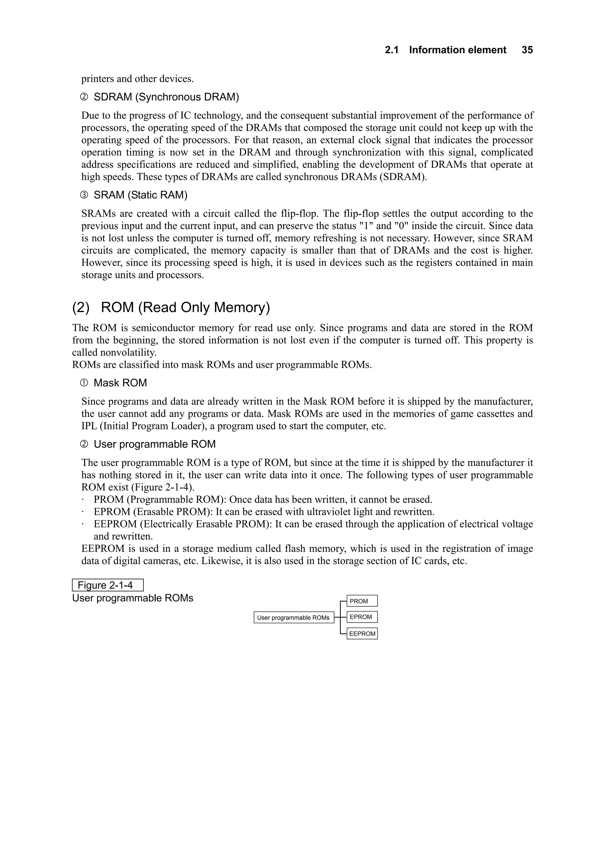
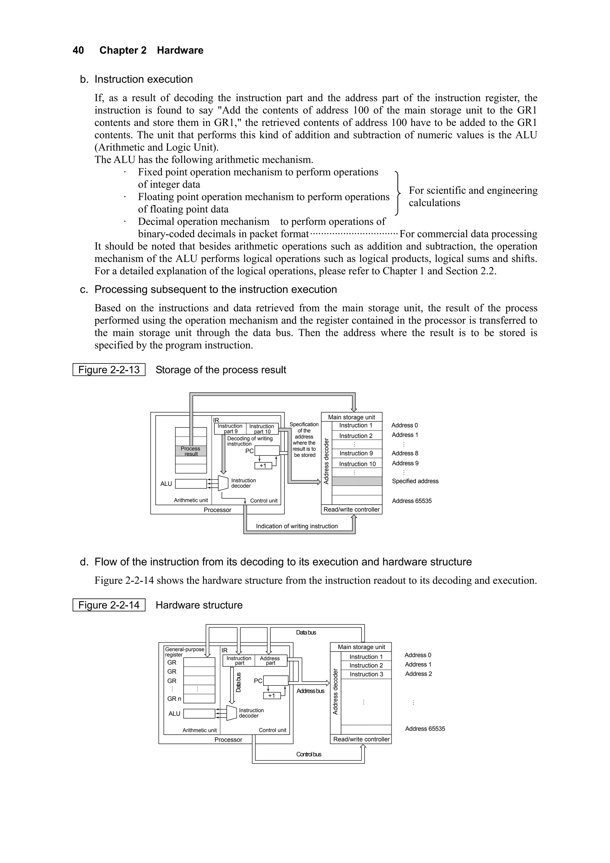
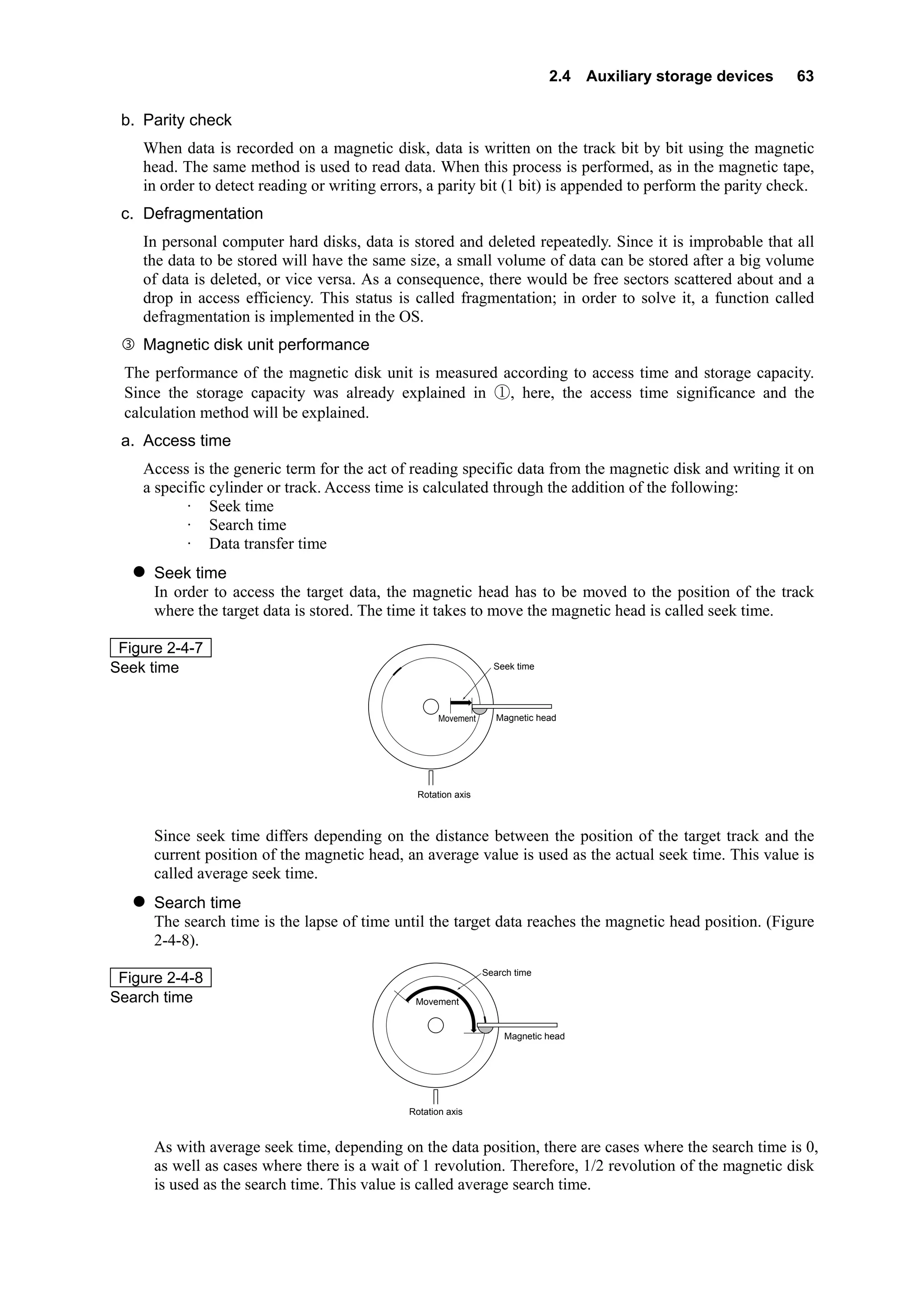
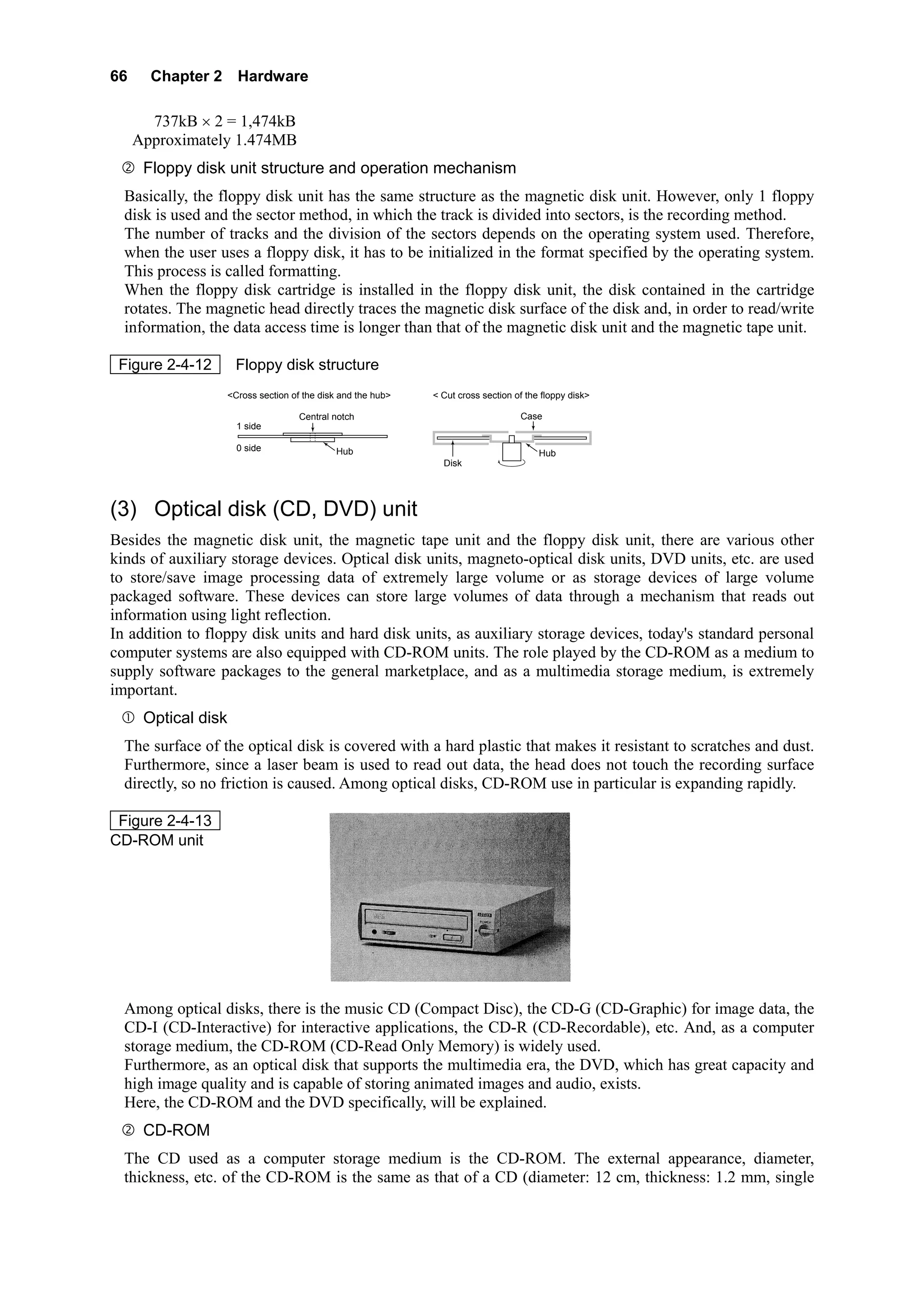
(2) Floppy disk unit
The floppy disk unit is also called a flexible disk unit. In floppy disk units data random access is possible,
and, since the floppy disk itself, which is a storage medium, is low-priced and easy to carry about, its use
has widely spread. As an auxiliary storage device of personal computers, it is the most ordinarily used
device.
Figure 2-4-9 <Floppy disk (0 side)> <Floppy disk (1 side)>
Floppy disk Head window
Shutter
Head window
Second standard notch
(Flexible disk)
Notch
First standard
notch
Case
Hub operative notch
Label area
Write-protect
notch
3.5 inches
(There are also disks of 5 inches and 8 inches)](https://image.slidesharecdn.com/no-1part1chap2-120309003504-phpapp02/75/Processor-architecture-33-2048.jpg)
![2.4 Auxiliary storage devices 65
The recording method of the floppy disk is the sector method, and as it is shown in Figure 2-4-10; the track
is divided into sectors, and the data is recorded on a sector basis.
Figure 2-4-10
Data recording side
of the floppy disk
Tracks
Sector
Floppy disk
a. Types
Among floppy disks, there are magnetic disks that measure 8 inches, 5 inches and 3.5 inches, but, the
most common disks today are 3.5 inch-disks, while 8- and 5-inch disks are almost never used. There are
also the following 2 types of 3.5-inch floppy disks, depending on the storage density.
· 3.5 inch 2 HD (double side High Density)
Storage capacity: 1.2 to 1.4 megabytes (MB)
· 3.5 inch 2 DD (double side Double Density)
Storage capacity: 640 to 730 kilobytes (kB)
Figure 2-4-11 1.4MB 1.2MB
Example of the specifications Sides available for use 2 2
of a floppy disk (2HD) Track number/side 80 77
Sector number/track 18 8
Storage capacity (B)/sector 512 1,024
Likewise, there is a floppy disk whose storage capacity is 120MB (UHD) and a disk called Zip whose
storage capacity is 100MB. Both of them are compatible with the 3.5-inch disk (2DD/2HD), but they have
not come into wide use.
b. Storage capacity
The calculation of the access time of floppy disk units is the same as that for magnetic disk units.
Therefore, here, the storage capacity of the sector method will be explained.
As was shown in Figure 2-4-11, among floppy disks, the sides available for use, the number of tracks
per side, the number of sectors per track, etc. differ.
The storage capacity of a floppy disk is calculated using the following values:
Storage capacity per sector × Number of sectors per track × Number of tracks per side ×
Number of sides (One side or both sides)
Example
Given a floppy disk with the following specifications, the storage capacity is calculated.
[Specification of a floppy disk unit]
• Sides available for use: 2 sides
• Track number/side: 80 tracks
• Sector number/track: 9 sectors
• Storage capacity/sector: 1,024 bytes
The storage capacity of 1 track is as follows:
1,024 bytes/sector × 9 sectors/track = 9,216 bytes/track
Therefore, the storage capacity of 1 side is as follows:
9,216 bytes/track × 80 tracks = 737,280 bytes ≤ 737kB
And, since the sides available for use of the floppy disk are 2 (sides), the following is the storage
capacity:](https://image.slidesharecdn.com/no-1part1chap2-120309003504-phpapp02/75/Processor-architecture-34-2048.jpg)


![Ise iv-computer organization [10 cs46]-notes new](https://cdn.slidesharecdn.com/ss_thumbnails/ise-iv-computerorganization10cs46-notesnew-140624013827-phpapp01-thumbnail.jpg?width=640&height=640&fit=bounds)


