Downloaded 620 times
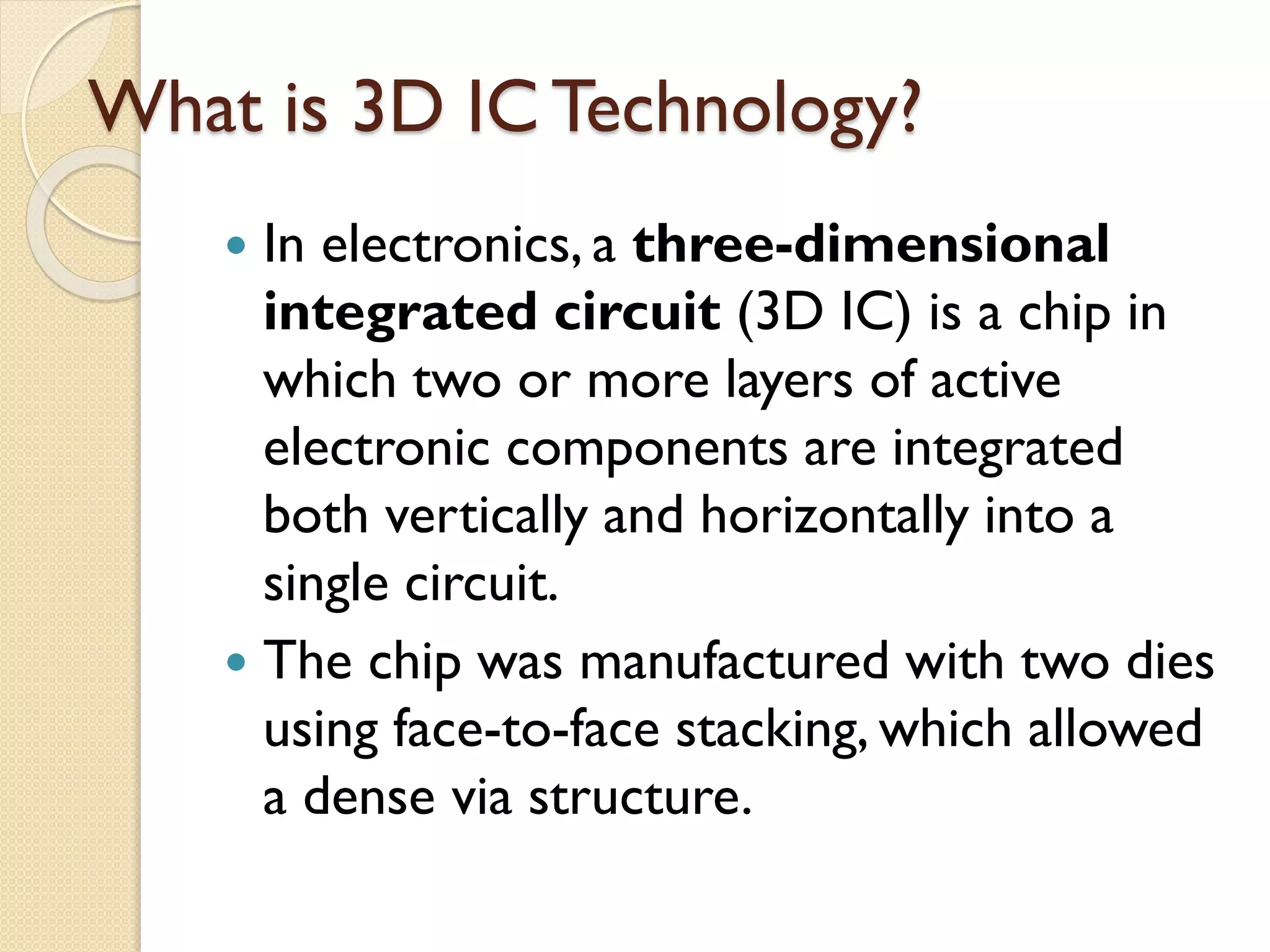
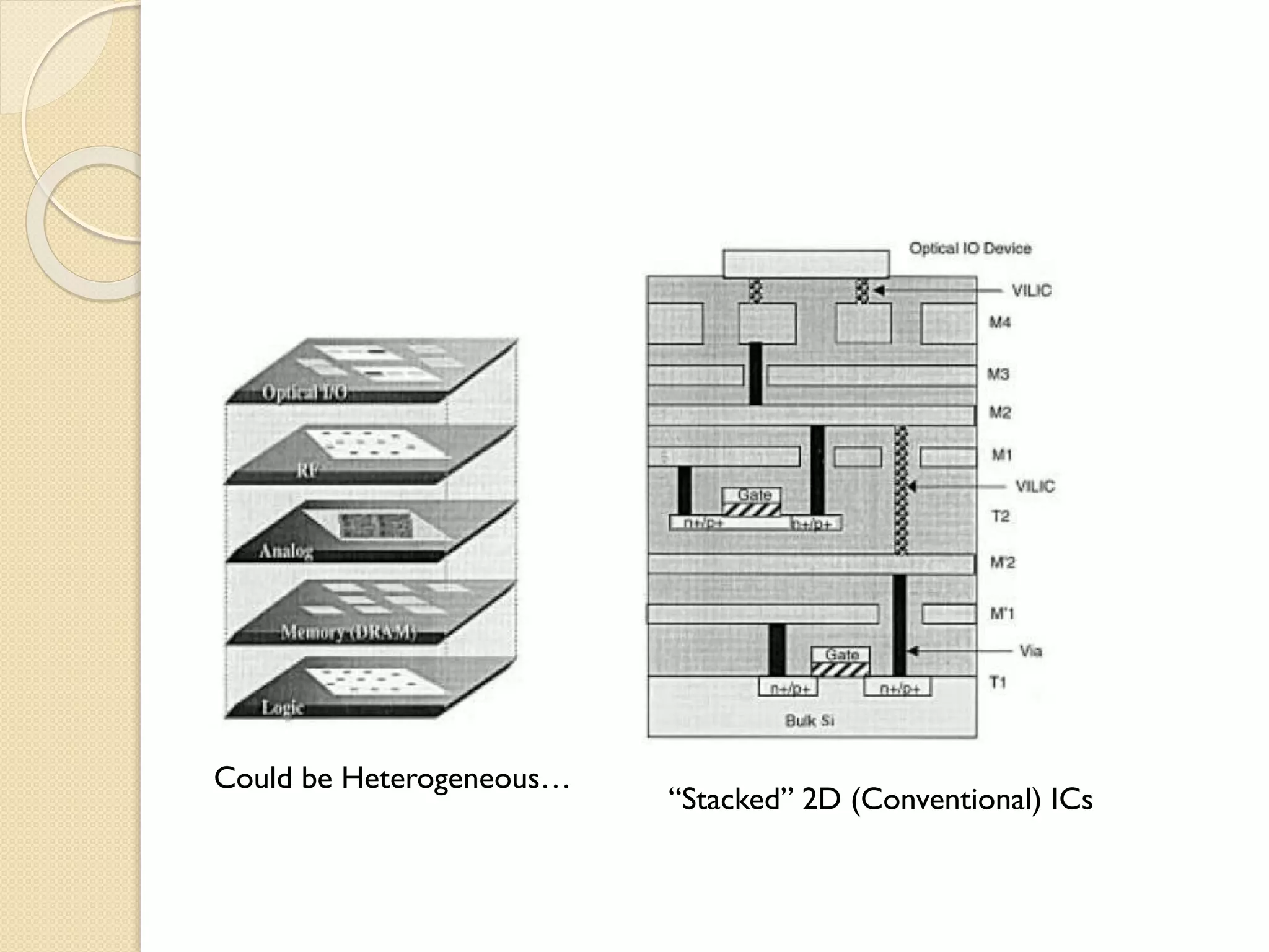
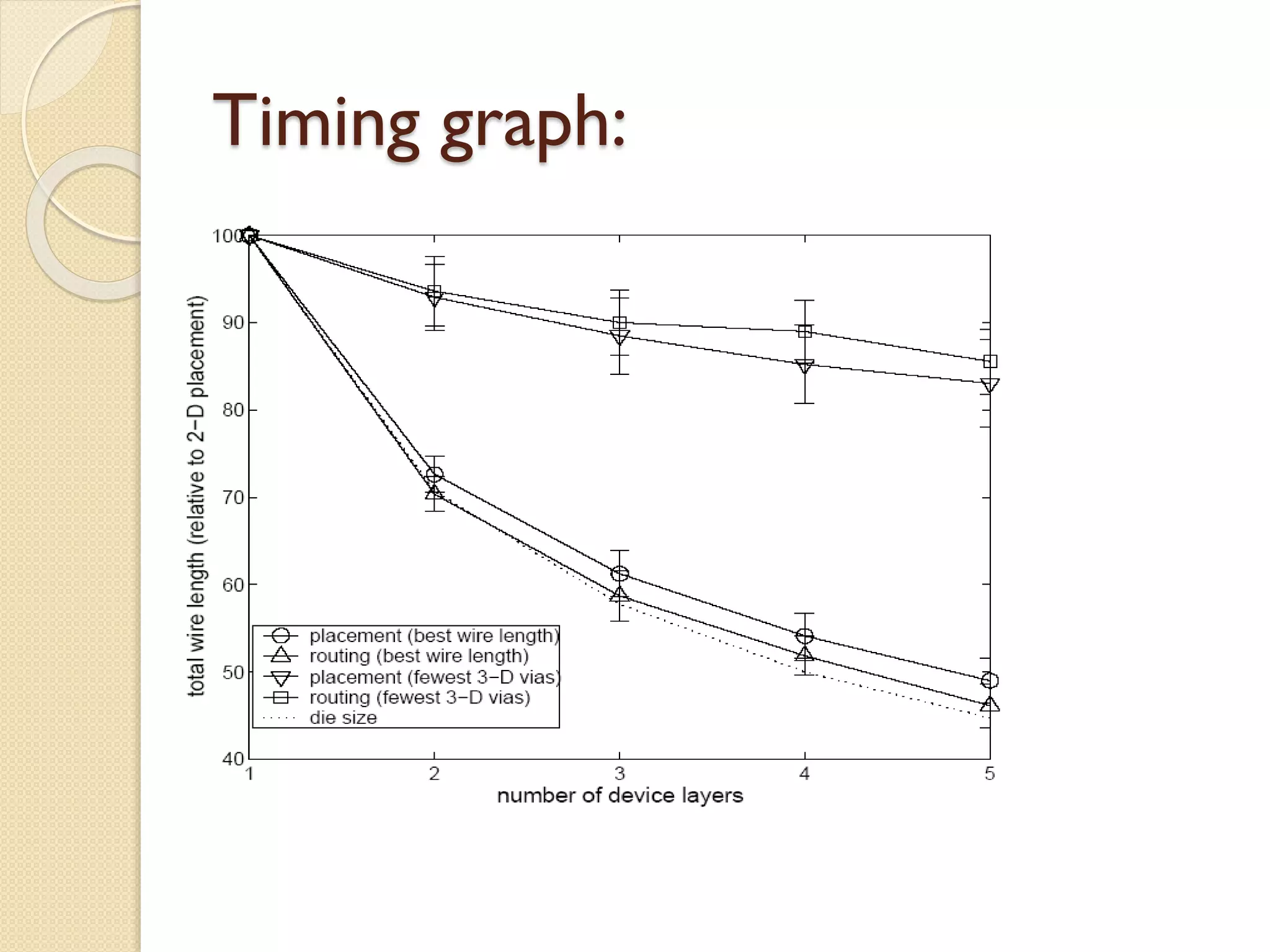
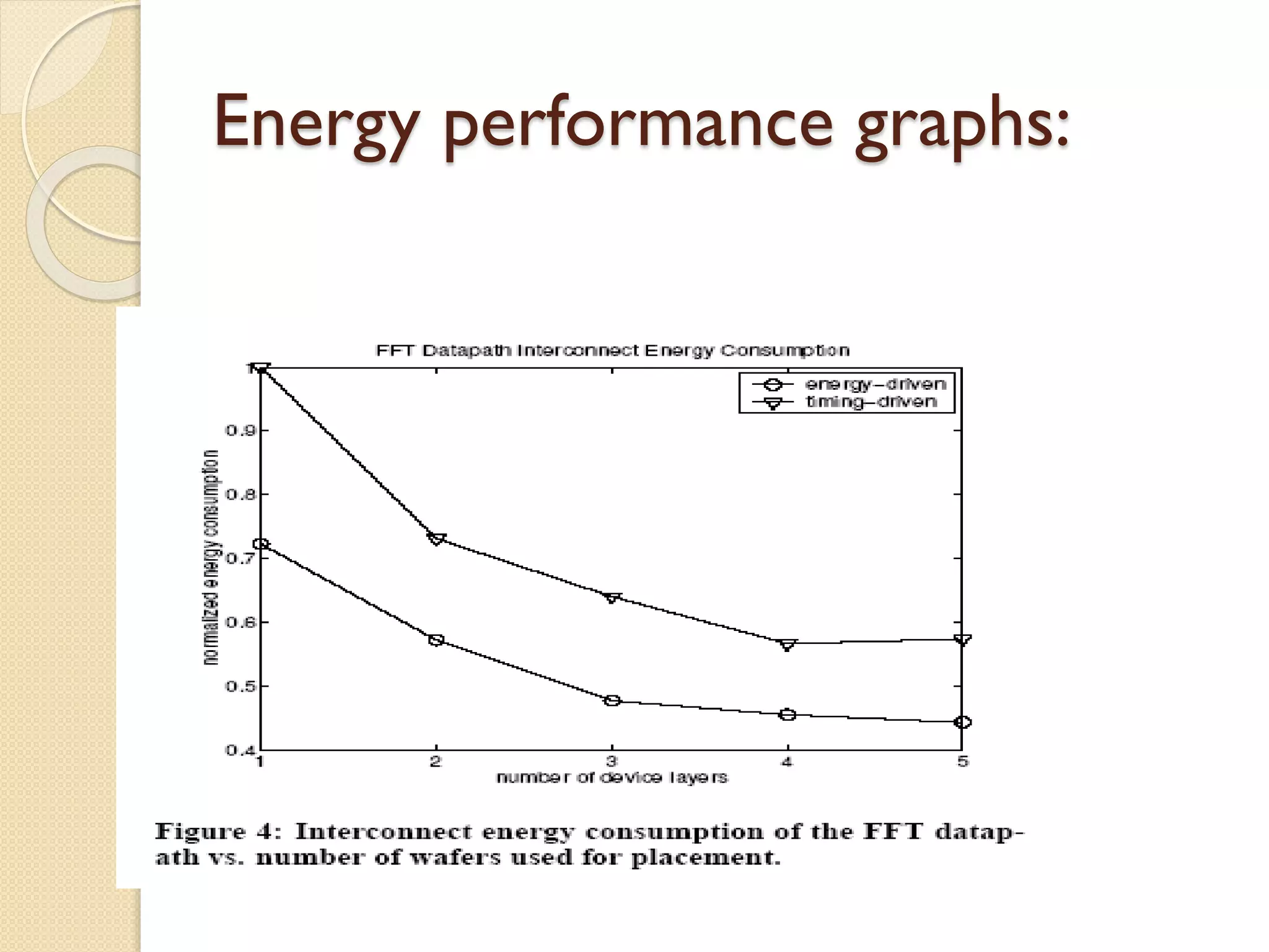
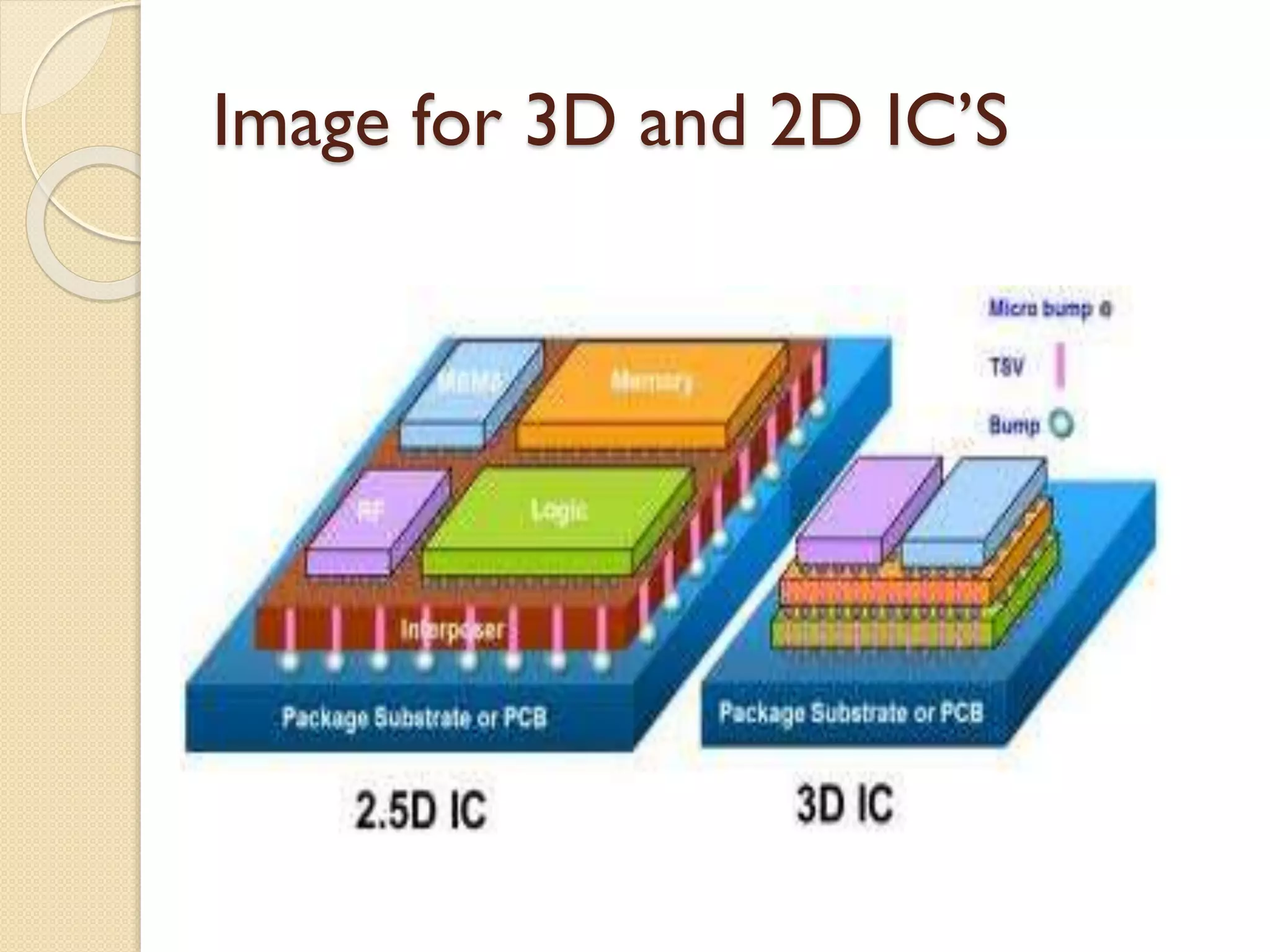
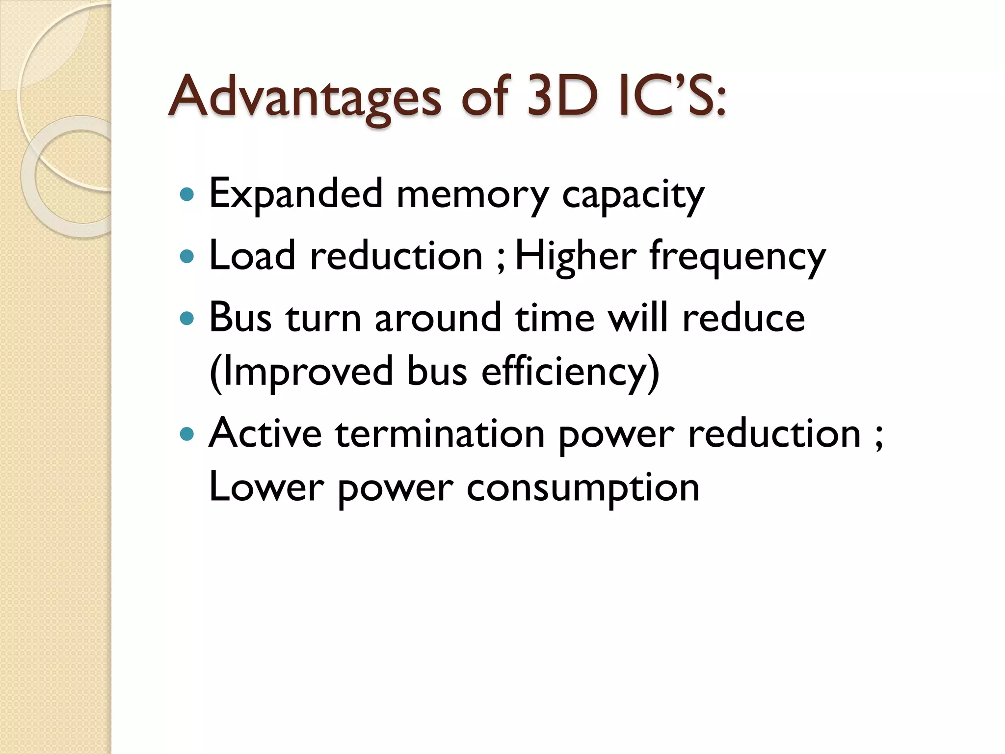
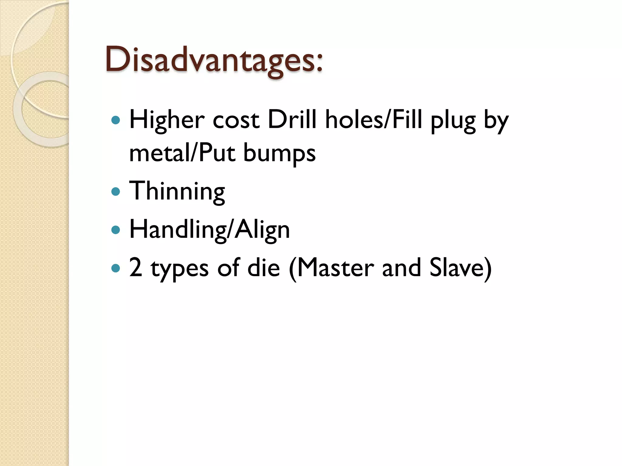


This document summarizes a technical seminar on 3D IC technology. It defines 3D ICs as having two or more layers of electronic components integrated vertically and horizontally. 3D ICs offer performance benefits like reduced timing/delays and energy usage due to shorter interconnects compared to conventional 2D chip designs. However, 3D ICs also present challenges like increased costs, handling issues during manufacturing, heat dissipation, complex design/testing, and lack of standards.