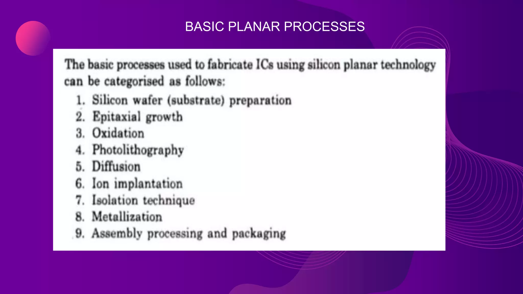
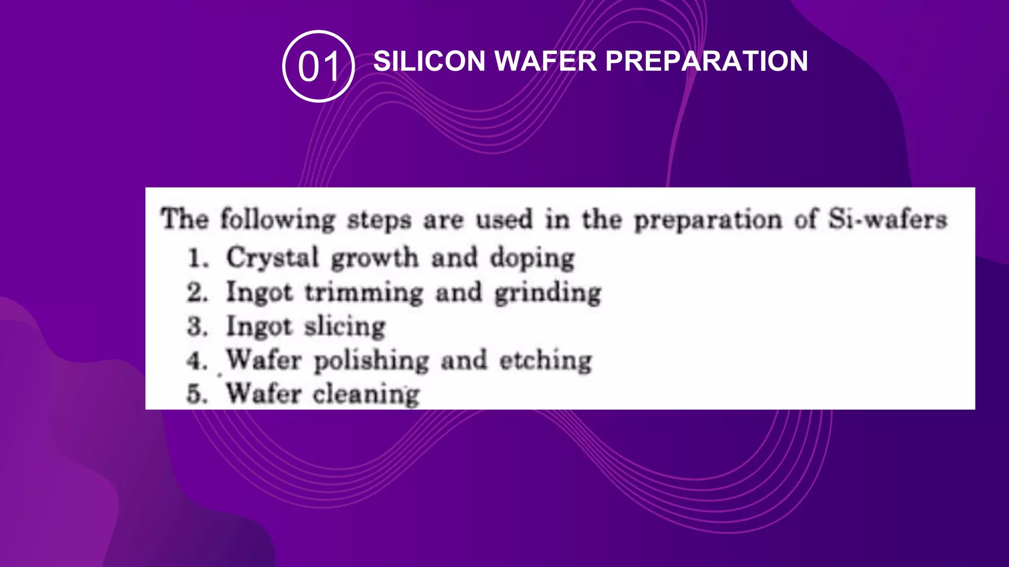
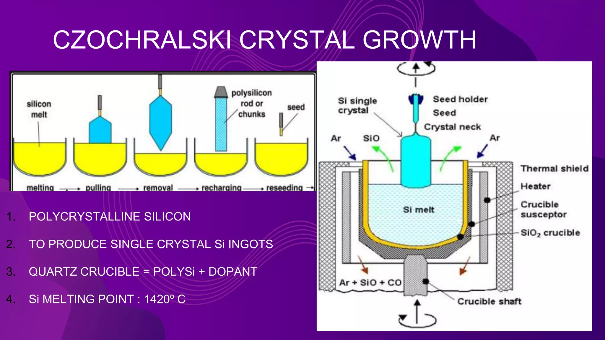
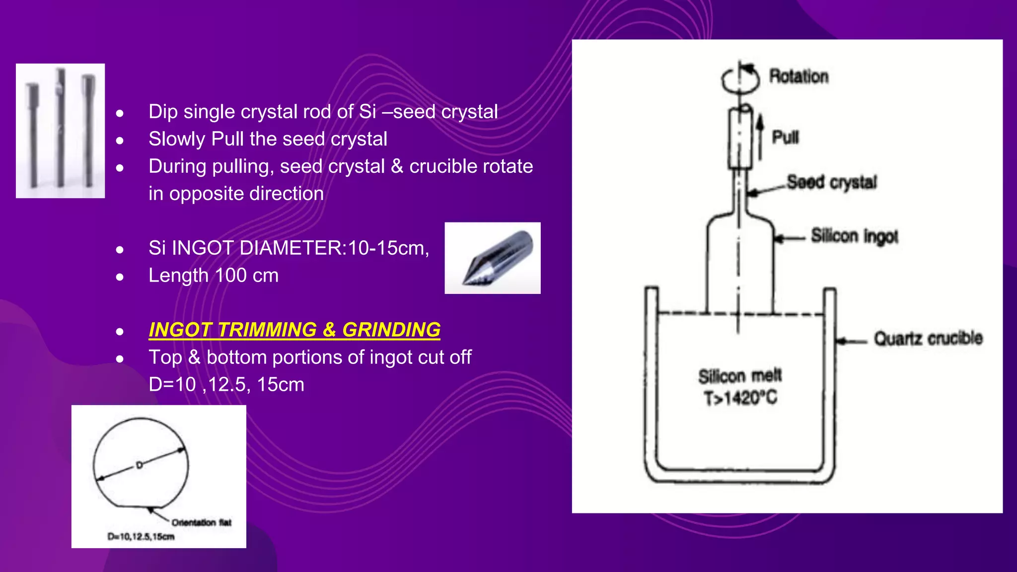
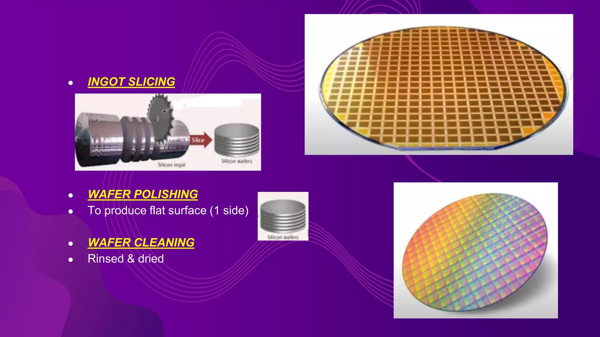
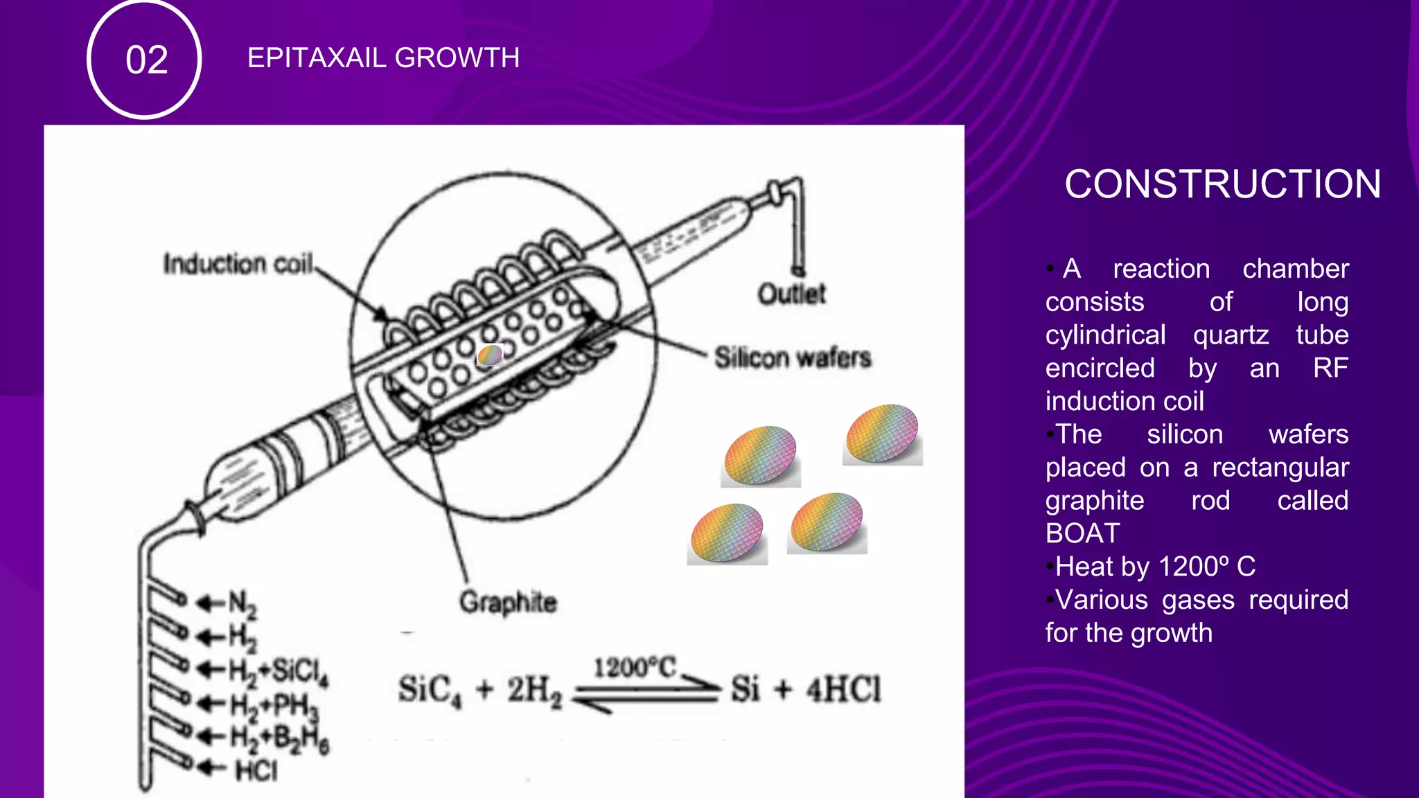
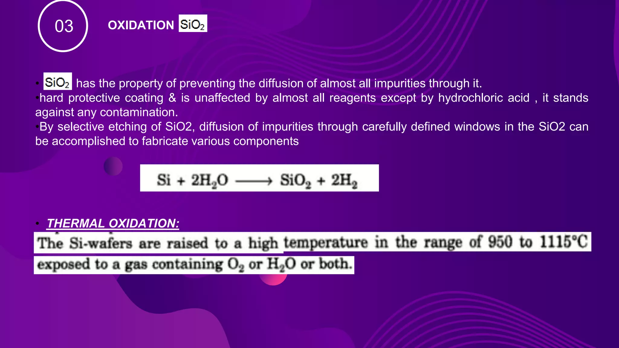
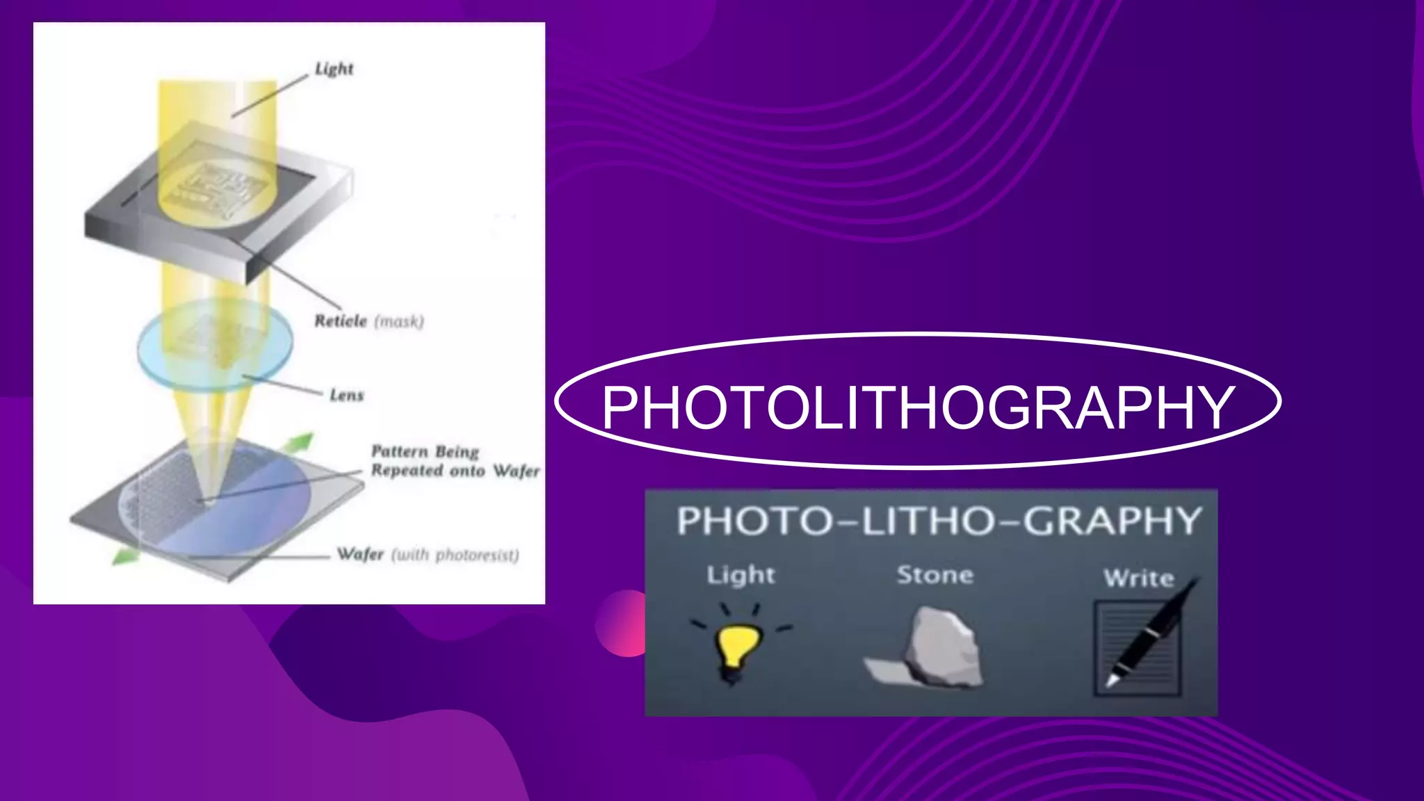
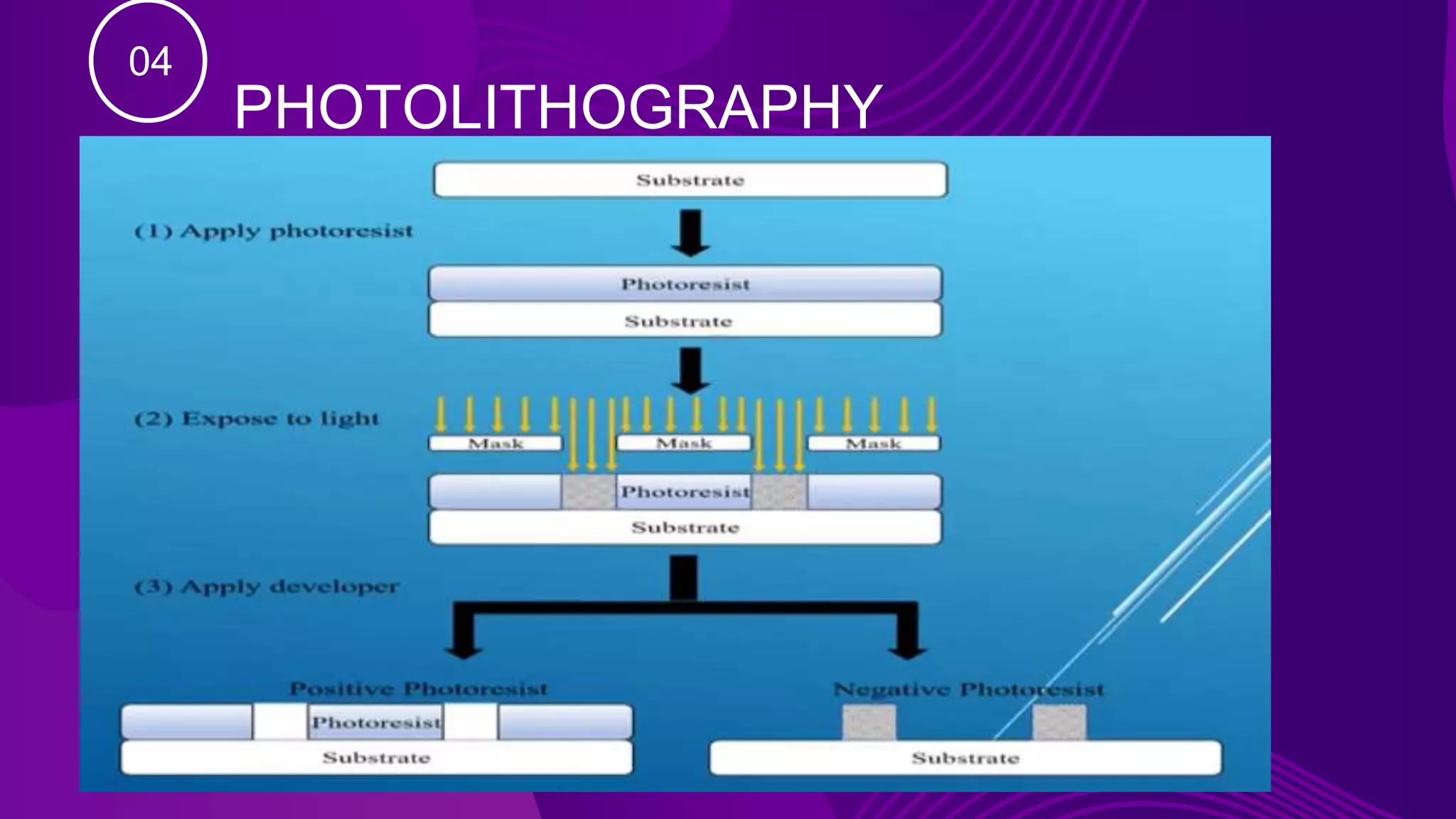
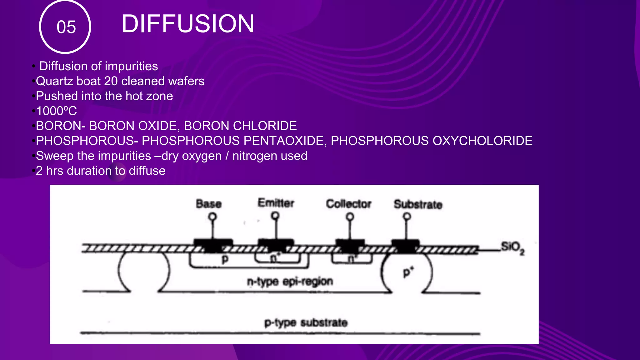
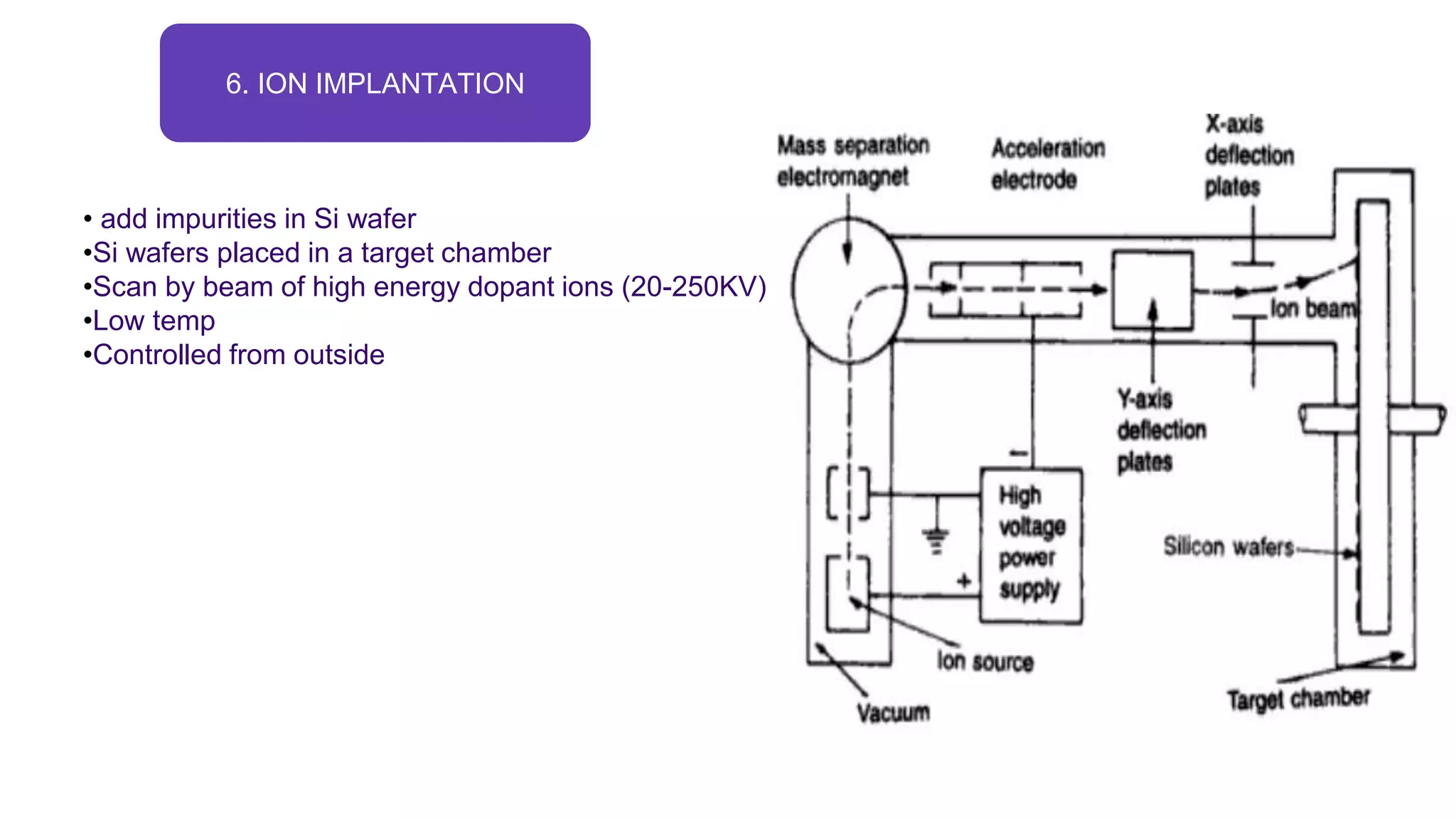
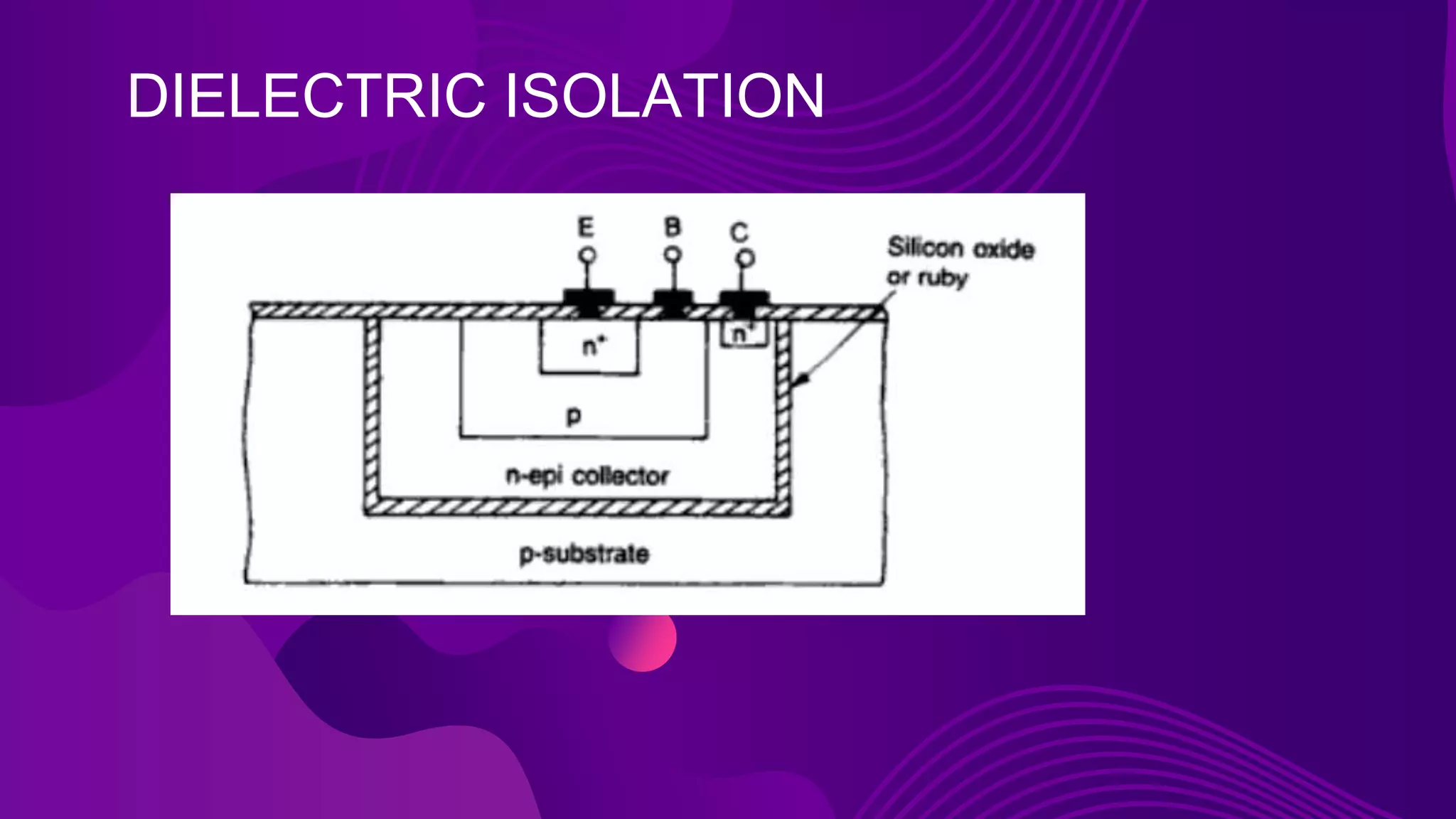
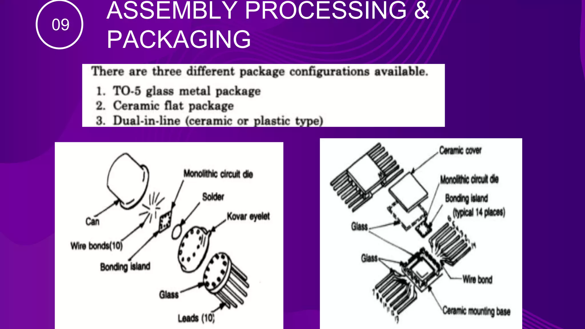
FABRICATION OF
MONOLITHIC IC
TECHNOLOGY
Mr .C.KARTHIKEYAN,
ASSISTANT PROFESSOR,
ECE, RMKCET
BASIC PLANAR PROCESSES
01 SILICON WAFER PREPARATION
CZOCHRALSKI CRYSTAL GROWTH
1. POLYCRYSTALLINE SILICON
2. TO PRODUCE SINGLE CRYSTAL Si INGOTS
3. QUARTZ CRUCIBLE = POLYSi + DOPANT
4. Si MELTING POINT : 1420º C
● Dip single crystal rod of Si –seed crystal
● Slowly Pull the seed crystal
● During pulling, seed crystal & crucible rotate
in opposite direction
● Si INGOT DIAMETER:10-15cm,
● Length 100 cm
● INGOT TRIMMING & GRINDING
● Top & bottom portions of ingot cut off
D=10 ,12.5, 15cm
● INGOT SLICING
● WAFER POLISHING
● To produce flat surface (1 side)
● WAFER CLEANING
● Rinsed & dried
EPITAXAIL GROWTH
EPI- upon
TAXY- arrangement
02 EPITAXAIL GROWTH
• A reaction chamber
consists of long
cylindrical quartz tube
encircled by an RF
induction coil
•The silicon wafers
placed on a rectangular
graphite rod called
BOAT
•Heat by 1200º C
•Various gases required
for the growth
CONSTRUCTION
03 OXIDATION
• has the property of preventing the diffusion of almost all impurities through it.
•hard protective coating & is unaffected by almost all reagents except by hydrochloric acid , it stands
against any contamination.
•By selective etching of SiO2, diffusion of impurities through carefully defined windows in the SiO2 can
be accomplished to fabricate various components
• THERMAL OXIDATION:
PHOTOLITHOGRAPHY
PHOTOLITHOGRAPHY
04
2 Processes:
(i) PHOTOGRAPHIC MASK – to generate the patterns
(ii) Photo etching – to remove from desired regions
• coat wafer with photosensitive emulsion
•Film thickness: 5000-10000Aº
•UV rays exposed – KPR Kodak photoresist to be polymerized
•Remove the mask
•Dip wafer in trichloroethylene chemical
•Pattern generated
•Dip in Hydrofluoric acid
•Removes silicondioxide
•TECHNIQUES
•X-ray
•Electron Beam Lithography
DIFFUSION
05
• Diffusion of impurities
•Quartz boat 20 cleaned wafers
•Pushed into the hot zone
•1000ºC
•BORON- BORON OXIDE, BORON CHLORIDE
•PHOSPHOROUS- PHOSPHOROUS PENTAOXIDE, PHOSPHOROUS OXYCHOLORIDE
•Sweep the impurities –dry oxygen / nitrogen used
•2 hrs duration to diffuse
Fonts & colors used
(https://fonts.google.com/specimen/Mukta)
#38076e #6e009a #861a97
#ffffff
6. ION IMPLANTATION
• add impurities in Si wafer
•Si wafers placed in a target chamber
•Scan by beam of high energy dopant ions (20-250KV)
•Low temp
•Controlled from outside
ISOLATION TECHNIQUES
07
•ISOLATION?
•2 Types
•(i) PN junction isolation
•Creation of islands for n & p regions
DIELECTRIC ISOLATION
METALLIZATION
08
ASSEMBLY PROCESSING &
PACKAGING
09
THANKS!

Unit 1 ic fab

  • 1.
    FABRICATION OF MONOLITHIC IC TECHNOLOGY Mr.C.KARTHIKEYAN, ASSISTANT PROFESSOR, ECE, RMKCET
  • 2.
  • 3.
    01 SILICON WAFERPREPARATION
  • 4.
    CZOCHRALSKI CRYSTAL GROWTH 1.POLYCRYSTALLINE SILICON 2. TO PRODUCE SINGLE CRYSTAL Si INGOTS 3. QUARTZ CRUCIBLE = POLYSi + DOPANT 4. Si MELTING POINT : 1420º C
  • 5.
    ● Dip singlecrystal rod of Si –seed crystal ● Slowly Pull the seed crystal ● During pulling, seed crystal & crucible rotate in opposite direction ● Si INGOT DIAMETER:10-15cm, ● Length 100 cm ● INGOT TRIMMING & GRINDING ● Top & bottom portions of ingot cut off D=10 ,12.5, 15cm
  • 6.
    ● INGOT SLICING ●WAFER POLISHING ● To produce flat surface (1 side) ● WAFER CLEANING ● Rinsed & dried
  • 7.
  • 8.
    02 EPITAXAIL GROWTH •A reaction chamber consists of long cylindrical quartz tube encircled by an RF induction coil •The silicon wafers placed on a rectangular graphite rod called BOAT •Heat by 1200º C •Various gases required for the growth CONSTRUCTION
  • 9.
    03 OXIDATION • hasthe property of preventing the diffusion of almost all impurities through it. •hard protective coating & is unaffected by almost all reagents except by hydrochloric acid , it stands against any contamination. •By selective etching of SiO2, diffusion of impurities through carefully defined windows in the SiO2 can be accomplished to fabricate various components • THERMAL OXIDATION:
  • 10.
  • 11.
  • 12.
    2 Processes: (i) PHOTOGRAPHICMASK – to generate the patterns (ii) Photo etching – to remove from desired regions • coat wafer with photosensitive emulsion •Film thickness: 5000-10000Aº •UV rays exposed – KPR Kodak photoresist to be polymerized •Remove the mask •Dip wafer in trichloroethylene chemical •Pattern generated •Dip in Hydrofluoric acid •Removes silicondioxide •TECHNIQUES •X-ray •Electron Beam Lithography
  • 13.
    DIFFUSION 05 • Diffusion ofimpurities •Quartz boat 20 cleaned wafers •Pushed into the hot zone •1000ºC •BORON- BORON OXIDE, BORON CHLORIDE •PHOSPHOROUS- PHOSPHOROUS PENTAOXIDE, PHOSPHOROUS OXYCHOLORIDE •Sweep the impurities –dry oxygen / nitrogen used •2 hrs duration to diffuse
  • 14.
    Fonts & colorsused (https://fonts.google.com/specimen/Mukta) #38076e #6e009a #861a97 #ffffff 6. ION IMPLANTATION • add impurities in Si wafer •Si wafers placed in a target chamber •Scan by beam of high energy dopant ions (20-250KV) •Low temp •Controlled from outside
  • 15.
    ISOLATION TECHNIQUES 07 •ISOLATION? •2 Types •(i)PN junction isolation •Creation of islands for n & p regions
  • 16.
  • 17.
  • 18.
  • 19.