P n junction.
•
0 likes•76 views
The document outlines the basic fabrication steps used in manufacturing integrated circuits: 1) Oxidation grows a silicon dioxide layer on the wafer which functions as an insulator and barrier for diffusion and implantation. Two common oxidation methods are dry and wet oxidation. 2) Lithography coats the wafer with photoresist which is exposed to ultraviolet light to define the geometry of the P-N junction. 3) Diffusion and ion implantation introduce opposite type impurities into the semiconductor to form the P-N junction, either through solid state diffusion or by accelerating impurity ions. 4) Metallization deposits metal films using physical or chemical vapor deposition to form contacts and interconnections, completing the P-N
Report
Share
Report
Share
Download to read offline

Recommended
Fabrication of complex shaped microparticles for self-assembly applications -...
This document discusses the fabrication and assembly of complex shaped microparticles for self-assembly applications. It summarizes that (1) photolithography is used to fabricate a variety of shapes of SU-8 microparticles including squares, cylinders, and hexagons, (2) these particles can be modified with fluorescence or metal coatings, and (3) initial assembly experiments using evaporation and liquid-liquid interfaces have shown promise, but a liquid-liquid interface method is proposed to better control the assembly of the complex shaped particles.
Unit 1 ic fab
The document discusses the basic processes involved in the fabrication of monolithic integrated circuits. It describes the key steps which include silicon wafer preparation using the Czochralski crystal growth technique, epitaxial growth, oxidation, photolithography, diffusion, ion implantation, isolation techniques, metallization, and assembly/packaging. The overall goal is to introduce various impurities into a silicon wafer in precise locations and patterns to create the different components of an integrated circuit such as transistors, resistors and interconnects on a single silicon chip.
FABRICATION PROCESS
Process of IC Fabrication with steps.
The content presented are taken from various sources and explained using my understanding.
Lecture4 nmos process
The document describes the fabrication process of NMOS transistors. It involves 10 main steps: 1) using a p-doped silicon substrate, 2) growing a thick silicon dioxide layer, 3) patterning using photoresist and masks to expose areas for doping, 4) doping exposed areas to form the source and drain, 5) growing a thin silicon dioxide layer, 6) depositing polysilicon and patterning it to form the gate, 7) growing contacts through another oxide layer, and 8) depositing metal to connect the gate, source and drain. The process is self-aligning and forms enhancement mode transistors, while an extra ion implantation step is needed to form depletion mode transistors that have
Xaioling Ding-NM
This document describes a simple method for creating patterned SiO2/TiO2 films through photo and chemical reactions at room temperature. TiO2 films are patterned using UV light and a photosensitive organic-titanium solution. SiO2 particles are precipitated from silicate solution by adjusting the pH, which are then deposited on the TiO2 films due to attraction between TiO2 and SiO2 surfaces. The films are characterized using SEM and EDS, showing uniform deposition of SiO2 crystals on TiO2. The SiO2 films are further modified with amino groups using aminosilane to enable protein immobilization applications.
Ic fab
An integrated circuit is a semiconductor wafer containing thousands of tiny resistors, capacitors and transistors. There are several key steps in the fabrication of integrated circuits:
1. Silicon wafers are created by slicing purified silicon crystals into thin discs.
2. A patterned oxide layer is formed on the wafer through a photolithography process using a mask to transfer circuit patterns to the wafer.
3. The wafer then undergoes several post-processing steps like dicing, die bonding, wire bonding and encapsulation before electrical testing verifies its functioning.
A NOVEL PRECURSOR IN PREPARATION AND CHARACTERIZATION OF NICKEL OXIDE (NIO) A...
Synthesis of Nickel Oxide (NiO) nanoparticles and cobalt oxide (CO3O4) materials synthesis by aqueous chemical growth (ACG) Techniques. Oxide based material having a wide band gap, and suitable for optical devices,Optoelectronic devices, UV photodetector, and Light emitting diode LEDs. The analysis
and characterizationof Nickel Oxide (NiO) and cobalt oxide (CO3O4) nanoparticles by(1) X-ray diffraction (XRD), (2) Scanning electron microscopy (SEM), and (3) Ultraviolet–visible (UV–Vis) spectroscopy.
High speed semiconductor devices
EPITAXY GROWTH TOPIC
MADE BY- ASHISH JOSHI
PONDHICHERRY UNIVERSITY
DEPARTMENT OF ELECTRONICS ENGINEERING
Vlsi assembly technology
The document discusses VLSI assembly technology and the fabrication process for integrated circuits. It describes the key steps in assembly such as wafer back grinding, die preparation, die bonding, wire bonding, flip chip bonding, molding, package sealing, marking, and singulation. It also summarizes the major steps in IC fabrication including silicon crystal growth, lithography, oxidation, etching, diffusion/implantation, and annealing.
Manufacturing of microprocessor
The manufacturing of microprocessors involves growing pure silicon crystals, slicing wafers, and fabricating integrated circuits through repeated photolithography, etching, deposition, and doping steps in a clean room environment. Key steps include slicing silicon ingots into wafers, layering and patterning materials like insulators and conductors through photolithography and etching, and implanting dopants using ion implantation. After fabrication, the wafers are tested, cut into chips, and packaged into protective casings before use in electronic devices.
MONOLITHIC IC PROCESSES ppt.pptx
MONOLITHIC IC PROCESSES A monolithic integrated circuit (IC) is a set of circuitry on a single semiconductor plate or chip rather than built of separate elements as a discrete circuit is.
Unit-6 Semiconductor Manufacturing Process.pptx
The document discusses integrated circuit fabrication processes. It introduces basic steps like oxidation, diffusion, ion implantation, deposition, etching, and epitaxy. Photolithography is used to apply these steps selectively through masking. The fabrication process involves growing thin oxides, doping silicon through diffusion or implantation, depositing materials, and selectively removing layers with etching. Top-down and bottom-up are two approaches, with top-down using masking and etching and bottom-up growing structures from seed crystals or polymers.
2.ic fabrication
An integrated circuit consists of active and passive components fabricated together on a single crystal of silicon. It offers advantages like miniaturization, cost reduction, improved reliability and performance. The basic processes to fabricate monolithic ICs include silicon wafer preparation, epitaxial growth, oxidation, photolithography, diffusion, ion implantation, isolation techniques and metallization. Each process involves multiple steps to introduce impurities, create circuit patterns and interconnect components on a chip, which is then packaged.
Planar fabrication technology
This is one of the fabrication technology used in IC fabrication. This technique is mostly used in flexible electronics. It contains various other subprocesses in it.
How is a silicon substrate helpful to the electronics industry? What is it?
A semiconductor material that is extremely flat is used to make silicon substrate. It can be produced in a variety of ways, including the Float Zone (FZ) growing method and the Czochralski (CZ) pulling method.
https://waferpro.com/what-is-a-silicon-wafer/
Fabrication process flow
The document describes the key steps in the fabrication process of integrated circuits, including crystal growth, epitaxial growth, oxidation, doping, deposition, lithography, and etching. Crystal growth involves slowly withdrawing a silicon seed crystal from a melt of polycrystalline silicon to form a single crystal ingot. Epitaxial growth uses chemical vapor deposition or molecular beam epitaxy to form single-crystal layers on a substrate. Oxidation grows silicon dioxide layers via thermal oxidation. Doping introduces impurities via diffusion or ion implantation to modify conductivity. Lithography transfers circuit patterns to photoresist using a mask and photochemical processes.
silicon ic fabrican technology
This document describes the process for fabricating a silicon integrated circuit. It begins with an overview of the basic steps, which include cleaning silicon wafers, oxidation, photolithography, etching, diffusion, thin film deposition, and testing. It then focuses on the specific process for fabricating a P-N junction diode, outlining 10 steps: cleaning, oxidation, photolithography, etching, diffusion, metal deposition, photolithography, etching, contact formation, and testing. Diagrams and descriptions are provided for each step in the P-N diode fabrication process.
vlsi fabrication
The document discusses the key process steps in integrated circuit fabrication. It describes (1) preparing silicon wafers through processes like growing silicon crystals from sand and cutting the crystals into wafers, (2) diffusing impurities like boron and phosphorus into the wafers through high-temperature processes to dope the silicon, and (3) implanting ions of desired impurities into the wafers through acceleration and bombardment. The document also covers other important steps like annealing to activate the dopants, oxidizing the silicon to form insulating silicon dioxide layers, and lithography among others.
Epitaxial growth
This document provides information on various processes involved in integrated circuit fabrication, including epitaxial growth, oxidation, photolithography, diffusion, ion implantation, isolation techniques, and metallization. Epitaxial growth is used to grow silicon layers on substrates with the same crystal structure. Oxidation grows a silicon dioxide layer for protection and selective doping. Photolithography and etching are used to pattern doped regions. Diffusion and ion implantation introduce impurities. Isolation techniques like PN junctions and dielectric layers separate components. Metallization deposits aluminum for interconnections.
MOSFET fabrication 12
The document discusses the fabrication process of MOSFET transistors. It begins by introducing common semiconductor materials like silicon and compound semiconductors. Lithography is then described as the process of selectively patterning layers using a photomask and photoresist. The basic CMOS fabrication process involves growing oxide layers, creating wells, depositing polysilicon for gates, and doping the source and drain regions. Specifically, the n-MOS transistor fabrication process is outlined, showing the steps of oxidizing silicon, patterning field oxide, depositing gate oxide and polysilicon, doping the source and drain areas, and finally depositing contacts and interconnects.
IJSRED-V2I4P3
The document summarizes research on the effects of aging time of a silicon oxide (SiOx) sol-gel solution on the properties of nano crystalline silicon thin films produced using the sol-gel method. Nano silicon powders were mixed into a sol-gel of tetraethylorthosilicate and ethanol. The silicon dioxide films synthesized from this sol-gel were studied in terms of optical properties like refractive index by varying the aging time and annealing temperatures. The composition of the resulting SiOx films was found to vary from 1.1 to 2.0 as aging time increased. Characterization techniques like Raman spectroscopy, XRD, AFM and SEM were used to study the chemical composition, crystallinity and morphology of the
Oxidation
This document discusses oxidation growth kinetics in integrated circuit fabrication. It describes how silicon dioxide is formed through thermal oxidation of silicon wafers in oxygen or water vapor. Silicon dioxide is important in IC fabrication as it can act as an insulator, gate electrode in MOS devices, and provide electrical isolation. The growth rate of silicon dioxide is initially limited by the chemical reaction rate, then by the diffusion rate of oxygen or water molecules through the silicon dioxide layer. Impurities and processing parameters like temperature and exposure time are critical factors that influence the oxidation growth rate.
Fabrication of IC
The document summarizes key steps in the fabrication of integrated circuits: thermal oxidation grows a silicon dioxide layer on the wafer for diffusion barriers and insulation; photolithography patterns the oxide layer using a mask, photoresist, and etching; dopant diffusion introduces impurities into the silicon by heating to allow movement; and metal evaporation deposits a thin aluminum film to connect components. These process steps are precisely controlled to build up the circuit structures layer-by-layer on the silicon wafer.
REPORT
The document is a project report on Silicon on Insulator (SOI) devices submitted by two students, Kashish Grover and Sanket Gawade, to their professor. The report provides an overview of SOI technology, including the different manufacturing methods like SIMOX, Smart Cut, and ELTRAN processes. It describes the two main types of SOI devices - partially depleted SOI and fully depleted SOI. The students conducted simulations of SOI MOSFETs in SENTAURUS software and obtained the ID-VG characteristics. The report summarizes the key advantages of SOI devices like lower parasitic capacitance and better performance compared to conventional silicon substrates.
VLSI Design(Fabrication)
this ppt provides fabrication on SI wafer, CMOS fabrication process, basic CMOS inverter, future, application, advantage, disadvantage etc.
CMOS N-WELL.pptx
The document outlines the 20 step process for fabricating an N-well CMOS transistor on a silicon substrate. Key steps include:
1) Growing a silicon dioxide layer on the P-type substrate through oxidation.
2) Depositing and patterning a photoresist layer using a mask to selectively expose regions for diffusion.
3) Forming the N-well region by diffusing N-type impurities into the exposed areas of the substrate.
4) Depositing polysilicon and patterning it to form the transistor gates.
5) Creating source and drain regions through masked diffusion of N-type and P-type impurities.
6) Forming metal interconnections
Mems unit 1-lec_2
The basic steps of IC fabrication involve wafer production, epitaxial growth, etching, masking, doping, atomic diffusion, ion implantation, and metallization. These steps include growing high purity silicon crystals, slicing wafers, depositing and patterning layers, and adding impurities to alter conductivity. Lithography is used with photoresists and masks to pattern layers by selectively exposing and removing material. Oxidation forms insulating silicon dioxide layers through controlled heating processes. Etching then transfers the mask patterns by removing exposed material using wet chemical baths or plasma reactions.
The cost of acquiring information by natural selection
This is a short talk that I gave at the Banff International Research Station workshop on Modeling and Theory in Population Biology. The idea is to try to understand how the burden of natural selection relates to the amount of information that selection puts into the genome.
It's based on the first part of this research paper:
The cost of information acquisition by natural selection
Ryan Seamus McGee, Olivia Kosterlitz, Artem Kaznatcheev, Benjamin Kerr, Carl T. Bergstrom
bioRxiv 2022.07.02.498577; doi: https://doi.org/10.1101/2022.07.02.498577
More Related Content
Similar to P n junction.
Vlsi assembly technology
The document discusses VLSI assembly technology and the fabrication process for integrated circuits. It describes the key steps in assembly such as wafer back grinding, die preparation, die bonding, wire bonding, flip chip bonding, molding, package sealing, marking, and singulation. It also summarizes the major steps in IC fabrication including silicon crystal growth, lithography, oxidation, etching, diffusion/implantation, and annealing.
Manufacturing of microprocessor
The manufacturing of microprocessors involves growing pure silicon crystals, slicing wafers, and fabricating integrated circuits through repeated photolithography, etching, deposition, and doping steps in a clean room environment. Key steps include slicing silicon ingots into wafers, layering and patterning materials like insulators and conductors through photolithography and etching, and implanting dopants using ion implantation. After fabrication, the wafers are tested, cut into chips, and packaged into protective casings before use in electronic devices.
MONOLITHIC IC PROCESSES ppt.pptx
MONOLITHIC IC PROCESSES A monolithic integrated circuit (IC) is a set of circuitry on a single semiconductor plate or chip rather than built of separate elements as a discrete circuit is.
Unit-6 Semiconductor Manufacturing Process.pptx
The document discusses integrated circuit fabrication processes. It introduces basic steps like oxidation, diffusion, ion implantation, deposition, etching, and epitaxy. Photolithography is used to apply these steps selectively through masking. The fabrication process involves growing thin oxides, doping silicon through diffusion or implantation, depositing materials, and selectively removing layers with etching. Top-down and bottom-up are two approaches, with top-down using masking and etching and bottom-up growing structures from seed crystals or polymers.
2.ic fabrication
An integrated circuit consists of active and passive components fabricated together on a single crystal of silicon. It offers advantages like miniaturization, cost reduction, improved reliability and performance. The basic processes to fabricate monolithic ICs include silicon wafer preparation, epitaxial growth, oxidation, photolithography, diffusion, ion implantation, isolation techniques and metallization. Each process involves multiple steps to introduce impurities, create circuit patterns and interconnect components on a chip, which is then packaged.
Planar fabrication technology
This is one of the fabrication technology used in IC fabrication. This technique is mostly used in flexible electronics. It contains various other subprocesses in it.
How is a silicon substrate helpful to the electronics industry? What is it?
A semiconductor material that is extremely flat is used to make silicon substrate. It can be produced in a variety of ways, including the Float Zone (FZ) growing method and the Czochralski (CZ) pulling method.
https://waferpro.com/what-is-a-silicon-wafer/
Fabrication process flow
The document describes the key steps in the fabrication process of integrated circuits, including crystal growth, epitaxial growth, oxidation, doping, deposition, lithography, and etching. Crystal growth involves slowly withdrawing a silicon seed crystal from a melt of polycrystalline silicon to form a single crystal ingot. Epitaxial growth uses chemical vapor deposition or molecular beam epitaxy to form single-crystal layers on a substrate. Oxidation grows silicon dioxide layers via thermal oxidation. Doping introduces impurities via diffusion or ion implantation to modify conductivity. Lithography transfers circuit patterns to photoresist using a mask and photochemical processes.
silicon ic fabrican technology
This document describes the process for fabricating a silicon integrated circuit. It begins with an overview of the basic steps, which include cleaning silicon wafers, oxidation, photolithography, etching, diffusion, thin film deposition, and testing. It then focuses on the specific process for fabricating a P-N junction diode, outlining 10 steps: cleaning, oxidation, photolithography, etching, diffusion, metal deposition, photolithography, etching, contact formation, and testing. Diagrams and descriptions are provided for each step in the P-N diode fabrication process.
vlsi fabrication
The document discusses the key process steps in integrated circuit fabrication. It describes (1) preparing silicon wafers through processes like growing silicon crystals from sand and cutting the crystals into wafers, (2) diffusing impurities like boron and phosphorus into the wafers through high-temperature processes to dope the silicon, and (3) implanting ions of desired impurities into the wafers through acceleration and bombardment. The document also covers other important steps like annealing to activate the dopants, oxidizing the silicon to form insulating silicon dioxide layers, and lithography among others.
Epitaxial growth
This document provides information on various processes involved in integrated circuit fabrication, including epitaxial growth, oxidation, photolithography, diffusion, ion implantation, isolation techniques, and metallization. Epitaxial growth is used to grow silicon layers on substrates with the same crystal structure. Oxidation grows a silicon dioxide layer for protection and selective doping. Photolithography and etching are used to pattern doped regions. Diffusion and ion implantation introduce impurities. Isolation techniques like PN junctions and dielectric layers separate components. Metallization deposits aluminum for interconnections.
MOSFET fabrication 12
The document discusses the fabrication process of MOSFET transistors. It begins by introducing common semiconductor materials like silicon and compound semiconductors. Lithography is then described as the process of selectively patterning layers using a photomask and photoresist. The basic CMOS fabrication process involves growing oxide layers, creating wells, depositing polysilicon for gates, and doping the source and drain regions. Specifically, the n-MOS transistor fabrication process is outlined, showing the steps of oxidizing silicon, patterning field oxide, depositing gate oxide and polysilicon, doping the source and drain areas, and finally depositing contacts and interconnects.
IJSRED-V2I4P3
The document summarizes research on the effects of aging time of a silicon oxide (SiOx) sol-gel solution on the properties of nano crystalline silicon thin films produced using the sol-gel method. Nano silicon powders were mixed into a sol-gel of tetraethylorthosilicate and ethanol. The silicon dioxide films synthesized from this sol-gel were studied in terms of optical properties like refractive index by varying the aging time and annealing temperatures. The composition of the resulting SiOx films was found to vary from 1.1 to 2.0 as aging time increased. Characterization techniques like Raman spectroscopy, XRD, AFM and SEM were used to study the chemical composition, crystallinity and morphology of the
Oxidation
This document discusses oxidation growth kinetics in integrated circuit fabrication. It describes how silicon dioxide is formed through thermal oxidation of silicon wafers in oxygen or water vapor. Silicon dioxide is important in IC fabrication as it can act as an insulator, gate electrode in MOS devices, and provide electrical isolation. The growth rate of silicon dioxide is initially limited by the chemical reaction rate, then by the diffusion rate of oxygen or water molecules through the silicon dioxide layer. Impurities and processing parameters like temperature and exposure time are critical factors that influence the oxidation growth rate.
Fabrication of IC
The document summarizes key steps in the fabrication of integrated circuits: thermal oxidation grows a silicon dioxide layer on the wafer for diffusion barriers and insulation; photolithography patterns the oxide layer using a mask, photoresist, and etching; dopant diffusion introduces impurities into the silicon by heating to allow movement; and metal evaporation deposits a thin aluminum film to connect components. These process steps are precisely controlled to build up the circuit structures layer-by-layer on the silicon wafer.
REPORT
The document is a project report on Silicon on Insulator (SOI) devices submitted by two students, Kashish Grover and Sanket Gawade, to their professor. The report provides an overview of SOI technology, including the different manufacturing methods like SIMOX, Smart Cut, and ELTRAN processes. It describes the two main types of SOI devices - partially depleted SOI and fully depleted SOI. The students conducted simulations of SOI MOSFETs in SENTAURUS software and obtained the ID-VG characteristics. The report summarizes the key advantages of SOI devices like lower parasitic capacitance and better performance compared to conventional silicon substrates.
VLSI Design(Fabrication)
this ppt provides fabrication on SI wafer, CMOS fabrication process, basic CMOS inverter, future, application, advantage, disadvantage etc.
CMOS N-WELL.pptx
The document outlines the 20 step process for fabricating an N-well CMOS transistor on a silicon substrate. Key steps include:
1) Growing a silicon dioxide layer on the P-type substrate through oxidation.
2) Depositing and patterning a photoresist layer using a mask to selectively expose regions for diffusion.
3) Forming the N-well region by diffusing N-type impurities into the exposed areas of the substrate.
4) Depositing polysilicon and patterning it to form the transistor gates.
5) Creating source and drain regions through masked diffusion of N-type and P-type impurities.
6) Forming metal interconnections
Mems unit 1-lec_2
The basic steps of IC fabrication involve wafer production, epitaxial growth, etching, masking, doping, atomic diffusion, ion implantation, and metallization. These steps include growing high purity silicon crystals, slicing wafers, depositing and patterning layers, and adding impurities to alter conductivity. Lithography is used with photoresists and masks to pattern layers by selectively exposing and removing material. Oxidation forms insulating silicon dioxide layers through controlled heating processes. Etching then transfers the mask patterns by removing exposed material using wet chemical baths or plasma reactions.
Similar to P n junction. (20)
How is a silicon substrate helpful to the electronics industry? What is it?
How is a silicon substrate helpful to the electronics industry? What is it?
Recently uploaded
The cost of acquiring information by natural selection
This is a short talk that I gave at the Banff International Research Station workshop on Modeling and Theory in Population Biology. The idea is to try to understand how the burden of natural selection relates to the amount of information that selection puts into the genome.
It's based on the first part of this research paper:
The cost of information acquisition by natural selection
Ryan Seamus McGee, Olivia Kosterlitz, Artem Kaznatcheev, Benjamin Kerr, Carl T. Bergstrom
bioRxiv 2022.07.02.498577; doi: https://doi.org/10.1101/2022.07.02.498577
Compexometric titration/Chelatorphy titration/chelating titration
Classification
Metal ion ion indicators
Masking and demasking reagents
Estimation of Magnisium sulphate
Calcium gluconate
Complexometric Titration/ chelatometry titration/chelating titration, introduction, Types-
1.Direct Titration
2.Back Titration
3.Replacement Titration
4.Indirect Titration
Masking agent, Demasking agents
formation of complex
comparition between masking and demasking agents,
Indicators/Metal ion indicators/ Metallochromic indicators/pM indicators,
Visual Technique,PM indicators (metallochromic), Indicators of pH, Redox Indicators
Instrumental Techniques-Photometry
Potentiometry
Miscellaneous methods.
Complex titration with EDTA.
Gadgets for management of stored product pests_Dr.UPR.pdf
Insectsplayamajorroleinthedeteriorationoffoodgrainscausingbothquantitativeandqualitativelosses
Wellprovedthatnogranariescanbefilledwithgrainswithoutinsectsastheharvestedproducecontainegg(or)larvae(or)pupae(or)adultinsectinthembecauseoffieldcarryoverinfestationwhichcannotbeavoidedindevelopingcountrieslikeIndia
Simpletechnologiesfortimelydetectionofinsectsinthestoredproduceandtherebyplantimelycontrolmeasures
Micronuclei test.M.sc.zoology.fisheries.
Current Ms word generated power point presentation covers major details about the micronuclei test. It's significance and assays to conduct it. It is used to detect the micronuclei formation inside the cells of nearly every multicellular organism. It's formation takes place during chromosomal sepration at metaphase.
8.Isolation of pure cultures and preservation of cultures.pdf
Isolation of pure culture, its various method.
在线办理(salfor毕业证书)索尔福德大学毕业证毕业完成信一模一样
学校原件一模一样【微信:741003700 】《(salfor毕业证书)索尔福德大学毕业证》【微信:741003700 】学位证,留信认证(真实可查,永久存档)原件一模一样纸张工艺/offer、雅思、外壳等材料/诚信可靠,可直接看成品样本,帮您解决无法毕业带来的各种难题!外壳,原版制作,诚信可靠,可直接看成品样本。行业标杆!精益求精,诚心合作,真诚制作!多年品质 ,按需精细制作,24小时接单,全套进口原装设备。十五年致力于帮助留学生解决难题,包您满意。
本公司拥有海外各大学样板无数,能完美还原。
1:1完美还原海外各大学毕业材料上的工艺:水印,阴影底纹,钢印LOGO烫金烫银,LOGO烫金烫银复合重叠。文字图案浮雕、激光镭射、紫外荧光、温感、复印防伪等防伪工艺。材料咨询办理、认证咨询办理请加学历顾问Q/微741003700
【主营项目】
一.毕业证【q微741003700】成绩单、使馆认证、教育部认证、雅思托福成绩单、学生卡等!
二.真实使馆公证(即留学回国人员证明,不成功不收费)
三.真实教育部学历学位认证(教育部存档!教育部留服网站永久可查)
四.办理各国各大学文凭(一对一专业服务,可全程监控跟踪进度)
如果您处于以下几种情况:
◇在校期间,因各种原因未能顺利毕业……拿不到官方毕业证【q/微741003700】
◇面对父母的压力,希望尽快拿到;
◇不清楚认证流程以及材料该如何准备;
◇回国时间很长,忘记办理;
◇回国马上就要找工作,办给用人单位看;
◇企事业单位必须要求办理的
◇需要报考公务员、购买免税车、落转户口
◇申请留学生创业基金
留信网认证的作用:
1:该专业认证可证明留学生真实身份
2:同时对留学生所学专业登记给予评定
3:国家专业人才认证中心颁发入库证书
4:这个认证书并且可以归档倒地方
5:凡事获得留信网入网的信息将会逐步更新到个人身份内,将在公安局网内查询个人身份证信息后,同步读取人才网入库信息
6:个人职称评审加20分
7:个人信誉贷款加10分
8:在国家人才网主办的国家网络招聘大会中纳入资料,供国家高端企业选择人才
The binding of cosmological structures by massless topological defects
Assuming spherical symmetry and weak field, it is shown that if one solves the Poisson equation or the Einstein field
equations sourced by a topological defect, i.e. a singularity of a very specific form, the result is a localized gravitational
field capable of driving flat rotation (i.e. Keplerian circular orbits at a constant speed for all radii) of test masses on a thin
spherical shell without any underlying mass. Moreover, a large-scale structure which exploits this solution by assembling
concentrically a number of such topological defects can establish a flat stellar or galactic rotation curve, and can also deflect
light in the same manner as an equipotential (isothermal) sphere. Thus, the need for dark matter or modified gravity theory is
mitigated, at least in part.
Travis Hills of MN is Making Clean Water Accessible to All Through High Flux ...
By harnessing the power of High Flux Vacuum Membrane Distillation, Travis Hills from MN envisions a future where clean and safe drinking water is accessible to all, regardless of geographical location or economic status.
Sexuality - Issues, Attitude and Behaviour - Applied Social Psychology - Psyc...
A proprietary approach developed by bringing together the best of learning theories from Psychology, design principles from the world of visualization, and pedagogical methods from over a decade of training experience, that enables you to: Learn better, faster!
ESA/ACT Science Coffee: Diego Blas - Gravitational wave detection with orbita...
ESA/ACT Science Coffee: Diego Blas - Gravitational wave detection with orbita...Advanced-Concepts-Team
Presentation in the Science Coffee of the Advanced Concepts Team of the European Space Agency on the 07.06.2024.
Speaker: Diego Blas (IFAE/ICREA)
Title: Gravitational wave detection with orbital motion of Moon and artificial
Abstract:
In this talk I will describe some recent ideas to find gravitational waves from supermassive black holes or of primordial origin by studying their secular effect on the orbital motion of the Moon or satellites that are laser ranged.快速办理(UAM毕业证书)马德里自治大学毕业证学位证一模一样
学校原件一模一样【微信:741003700 】《(UAM毕业证书)马德里自治大学毕业证学位证》【微信:741003700 】学位证,留信认证(真实可查,永久存档)原件一模一样纸张工艺/offer、雅思、外壳等材料/诚信可靠,可直接看成品样本,帮您解决无法毕业带来的各种难题!外壳,原版制作,诚信可靠,可直接看成品样本。行业标杆!精益求精,诚心合作,真诚制作!多年品质 ,按需精细制作,24小时接单,全套进口原装设备。十五年致力于帮助留学生解决难题,包您满意。
本公司拥有海外各大学样板无数,能完美还原。
1:1完美还原海外各大学毕业材料上的工艺:水印,阴影底纹,钢印LOGO烫金烫银,LOGO烫金烫银复合重叠。文字图案浮雕、激光镭射、紫外荧光、温感、复印防伪等防伪工艺。材料咨询办理、认证咨询办理请加学历顾问Q/微741003700
【主营项目】
一.毕业证【q微741003700】成绩单、使馆认证、教育部认证、雅思托福成绩单、学生卡等!
二.真实使馆公证(即留学回国人员证明,不成功不收费)
三.真实教育部学历学位认证(教育部存档!教育部留服网站永久可查)
四.办理各国各大学文凭(一对一专业服务,可全程监控跟踪进度)
如果您处于以下几种情况:
◇在校期间,因各种原因未能顺利毕业……拿不到官方毕业证【q/微741003700】
◇面对父母的压力,希望尽快拿到;
◇不清楚认证流程以及材料该如何准备;
◇回国时间很长,忘记办理;
◇回国马上就要找工作,办给用人单位看;
◇企事业单位必须要求办理的
◇需要报考公务员、购买免税车、落转户口
◇申请留学生创业基金
留信网认证的作用:
1:该专业认证可证明留学生真实身份
2:同时对留学生所学专业登记给予评定
3:国家专业人才认证中心颁发入库证书
4:这个认证书并且可以归档倒地方
5:凡事获得留信网入网的信息将会逐步更新到个人身份内,将在公安局网内查询个人身份证信息后,同步读取人才网入库信息
6:个人职称评审加20分
7:个人信誉贷款加10分
8:在国家人才网主办的国家网络招聘大会中纳入资料,供国家高端企业选择人才
(June 12, 2024) Webinar: Development of PET theranostics targeting the molecu...
(June 12, 2024) Webinar: Development of PET theranostics targeting the molecu...Scintica Instrumentation
Targeting Hsp90 and its pathogen Orthologs with Tethered Inhibitors as a Diagnostic and Therapeutic Strategy for cancer and infectious diseases with Dr. Timothy Haystead.EWOCS-I: The catalog of X-ray sources in Westerlund 1 from the Extended Weste...
Context. With a mass exceeding several 104 M⊙ and a rich and dense population of massive stars, supermassive young star clusters
represent the most massive star-forming environment that is dominated by the feedback from massive stars and gravitational interactions
among stars.
Aims. In this paper we present the Extended Westerlund 1 and 2 Open Clusters Survey (EWOCS) project, which aims to investigate
the influence of the starburst environment on the formation of stars and planets, and on the evolution of both low and high mass stars.
The primary targets of this project are Westerlund 1 and 2, the closest supermassive star clusters to the Sun.
Methods. The project is based primarily on recent observations conducted with the Chandra and JWST observatories. Specifically,
the Chandra survey of Westerlund 1 consists of 36 new ACIS-I observations, nearly co-pointed, for a total exposure time of 1 Msec.
Additionally, we included 8 archival Chandra/ACIS-S observations. This paper presents the resulting catalog of X-ray sources within
and around Westerlund 1. Sources were detected by combining various existing methods, and photon extraction and source validation
were carried out using the ACIS-Extract software.
Results. The EWOCS X-ray catalog comprises 5963 validated sources out of the 9420 initially provided to ACIS-Extract, reaching a
photon flux threshold of approximately 2 × 10⁻⁸ photons cm−2
s
−1
. The X-ray sources exhibit a highly concentrated spatial distribution,
with 1075 sources located within the central 1 arcmin. We have successfully detected X-ray emissions from 126 out of the 166 known
massive stars of the cluster, and we have collected over 71 000 photons from the magnetar CXO J164710.20-455217.
Recently uploaded (20)
The cost of acquiring information by natural selection
The cost of acquiring information by natural selection
GBSN - Biochemistry (Unit 6) Chemistry of Proteins
GBSN - Biochemistry (Unit 6) Chemistry of Proteins
Compexometric titration/Chelatorphy titration/chelating titration
Compexometric titration/Chelatorphy titration/chelating titration
Gadgets for management of stored product pests_Dr.UPR.pdf
Gadgets for management of stored product pests_Dr.UPR.pdf
8.Isolation of pure cultures and preservation of cultures.pdf
8.Isolation of pure cultures and preservation of cultures.pdf
The binding of cosmological structures by massless topological defects
The binding of cosmological structures by massless topological defects
Travis Hills of MN is Making Clean Water Accessible to All Through High Flux ...
Travis Hills of MN is Making Clean Water Accessible to All Through High Flux ...
Sexuality - Issues, Attitude and Behaviour - Applied Social Psychology - Psyc...
Sexuality - Issues, Attitude and Behaviour - Applied Social Psychology - Psyc...
ESA/ACT Science Coffee: Diego Blas - Gravitational wave detection with orbita...
ESA/ACT Science Coffee: Diego Blas - Gravitational wave detection with orbita...
(June 12, 2024) Webinar: Development of PET theranostics targeting the molecu...
(June 12, 2024) Webinar: Development of PET theranostics targeting the molecu...
EWOCS-I: The catalog of X-ray sources in Westerlund 1 from the Extended Weste...
EWOCS-I: The catalog of X-ray sources in Westerlund 1 from the Extended Weste...
P n junction.
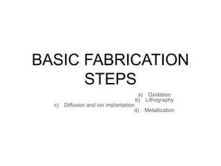
- 1. BASIC FABRICATION STEPS a) Oxidation b) Lithography c) Diffusion and ion implantation d) Metallization
- 2. Description 1) Oxidation: The development of high quality silicon dioxide(SiO2) has helped to establish the dominance of Si in the production of commercial ICs .Generally silicon dioxide functions as an insulator In a number of device structures or as a Barrier to diffusion or implantation in device fabrication. In fabrication of p-n junction the SiO2 film is used to define the junction area. There are two Sio2 growth methods,dry and wet oxidation. Fig:silicon Dioxide
- 3. 2) Lithography Another technology called photolithography is used to define the geometry of the P-N junction.After the formation of SiO2 wafer it is coted with an ultraviolet light sensitive material called photoresist.Which is spun on the surface of the wafer with a high speed spinner.
- 4. 3)Diffusion and Ion implantation In the diffusion process the semiconductor surface not protected by the oxide is exposed to a source with a high concentration of opposite type impurity.the impurity moves to the surface of the semiconductor crystal by solid state diffusion. In the Ion implantation method ,the intended impurity is introduced into the semiconductor by accelerating the impurity ions to a high energy level.
- 5. 4) Metallization After the Ion implantation process the mettalization process is continued toi form Ohmic contacts and interconnections.Metal film can be formed vby physical vapour deposition and chemical vapour deposition.with the completion of the metallization the P-N junction becomes functional.