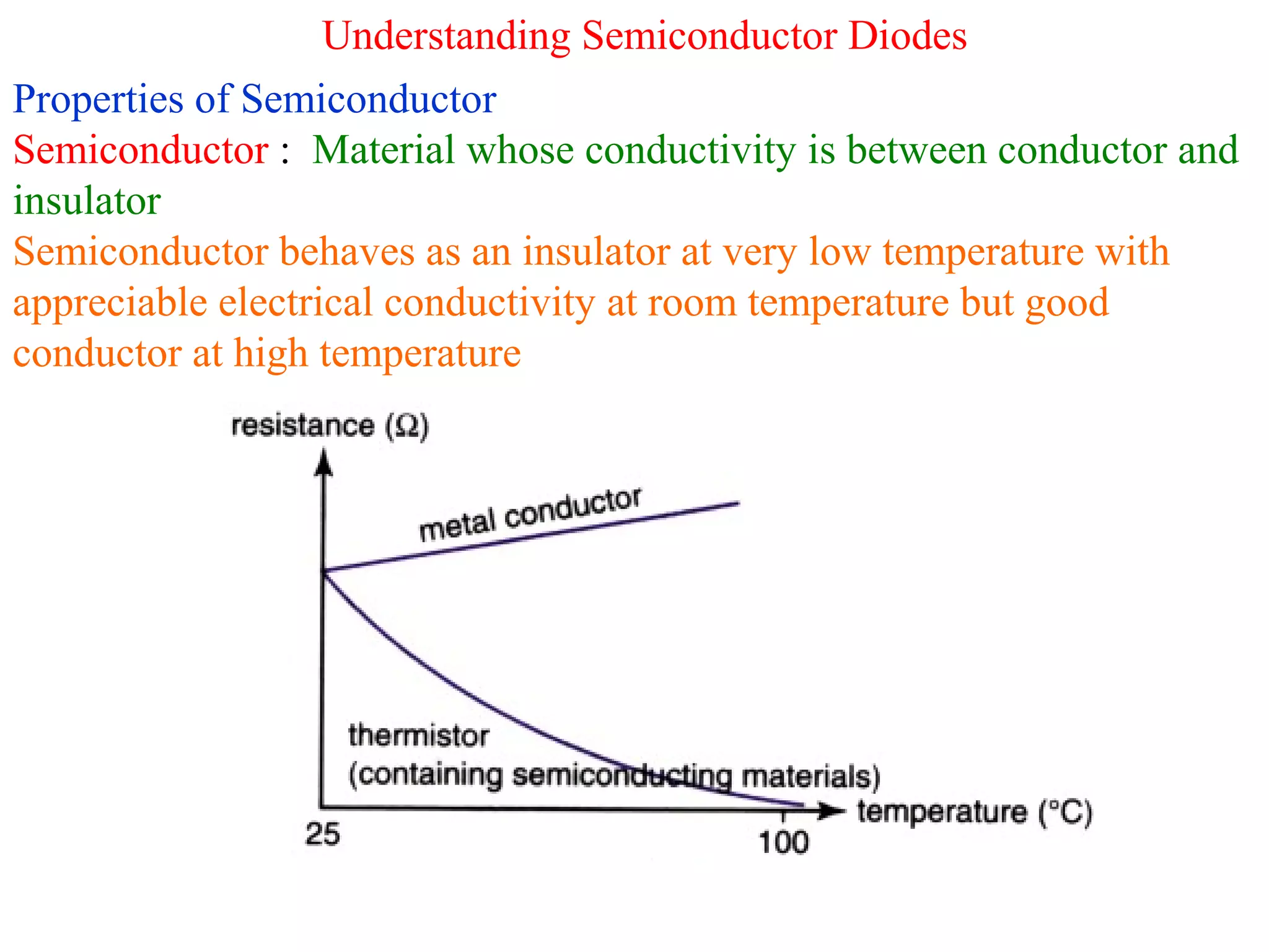
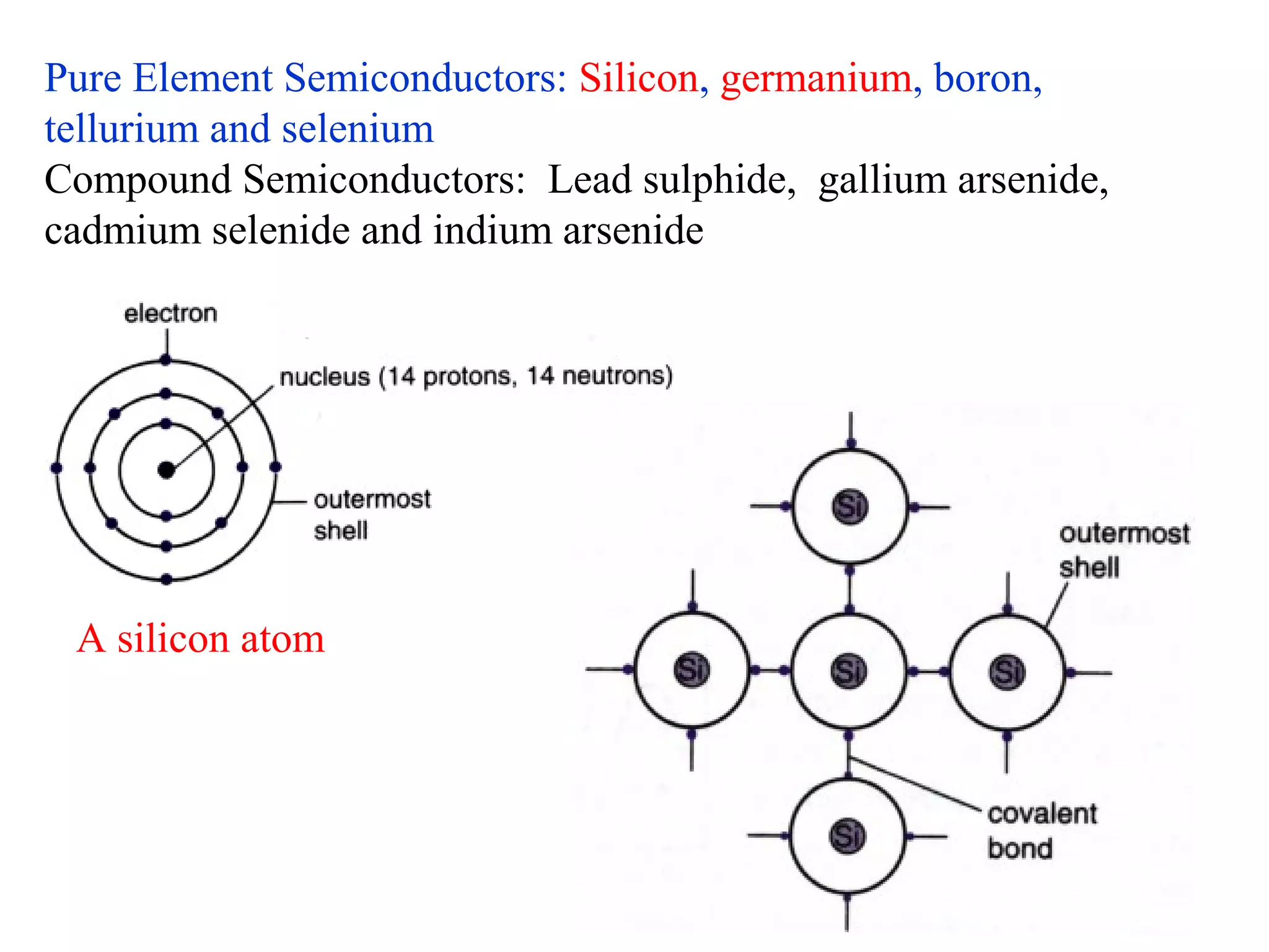
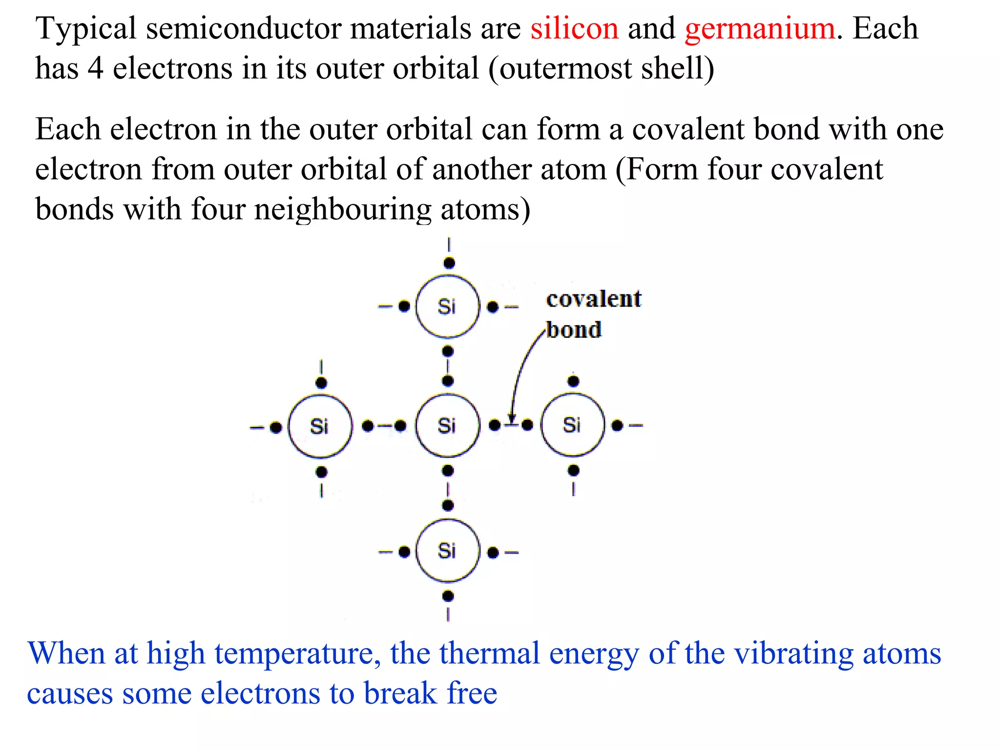
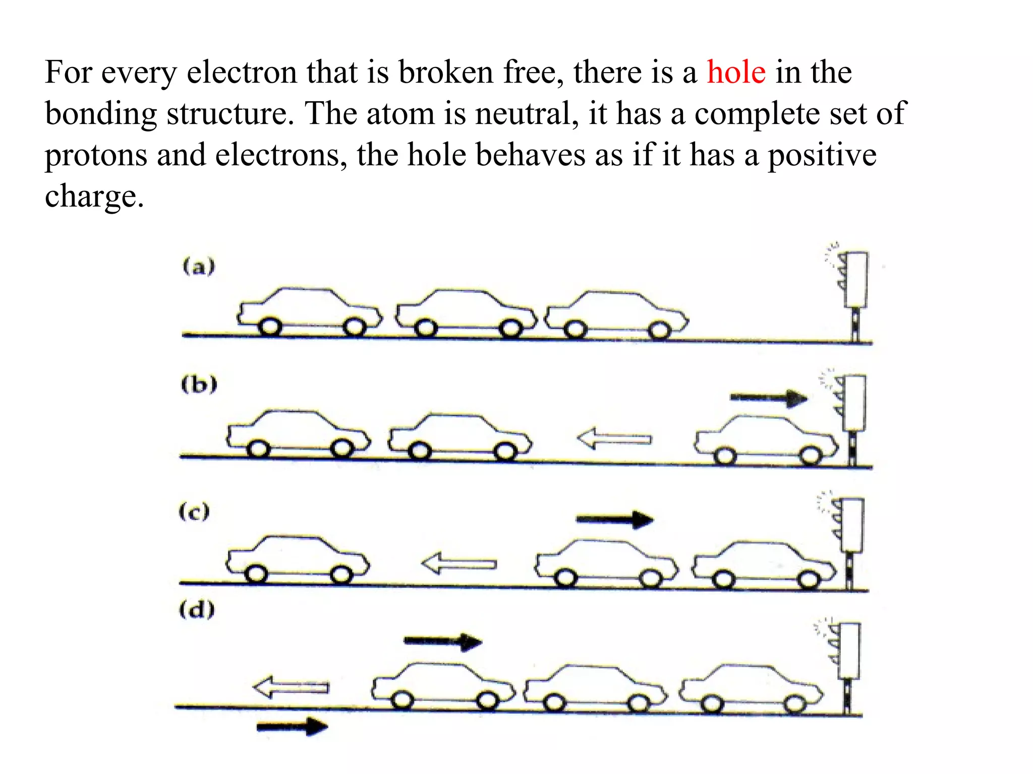
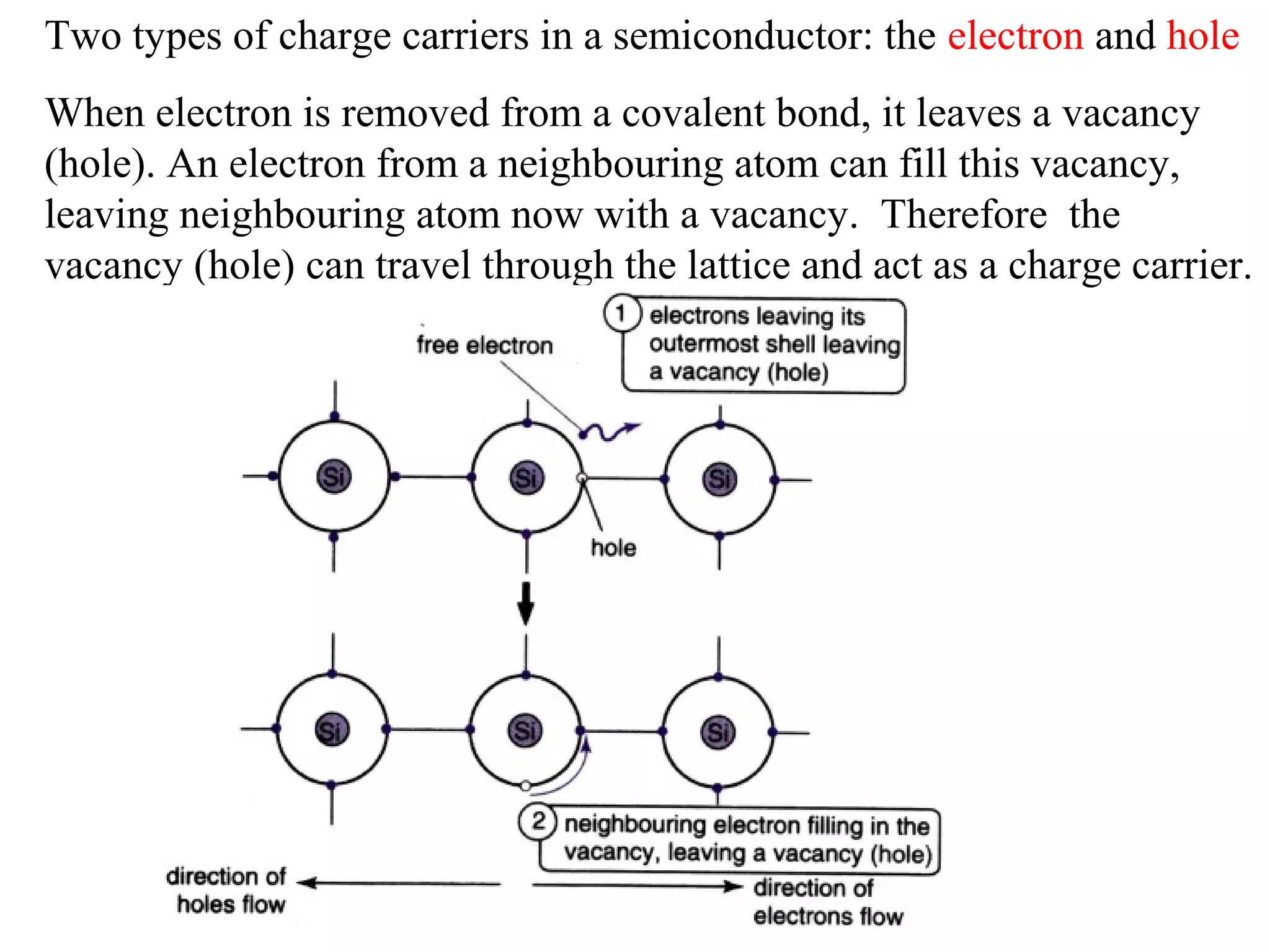
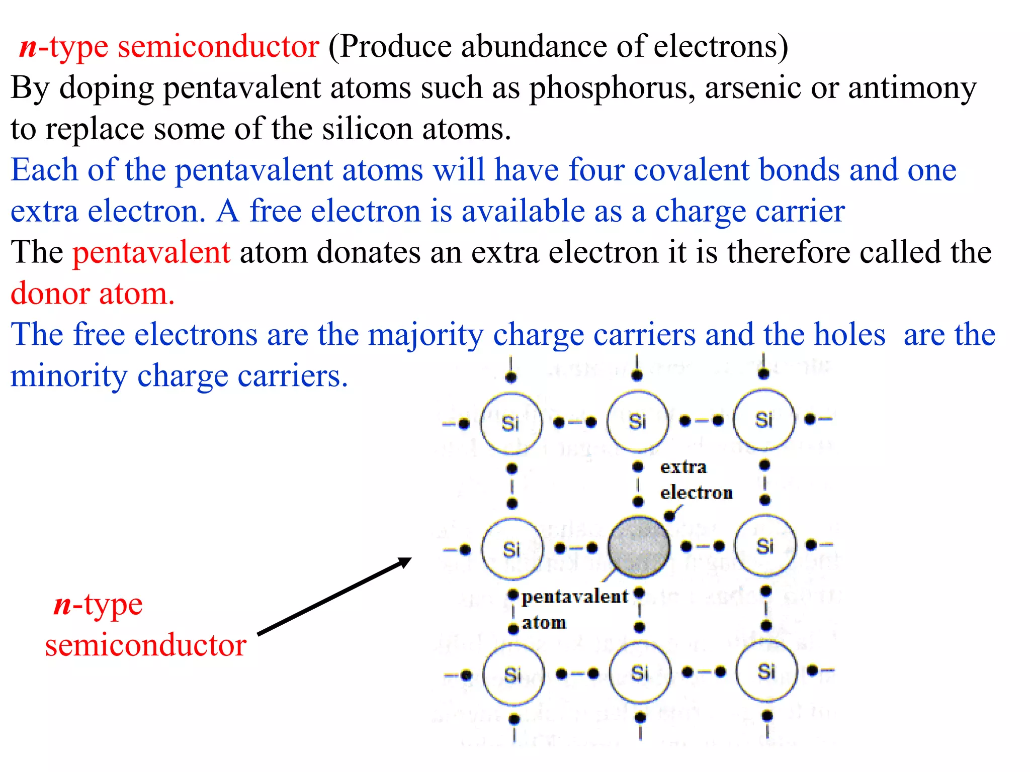
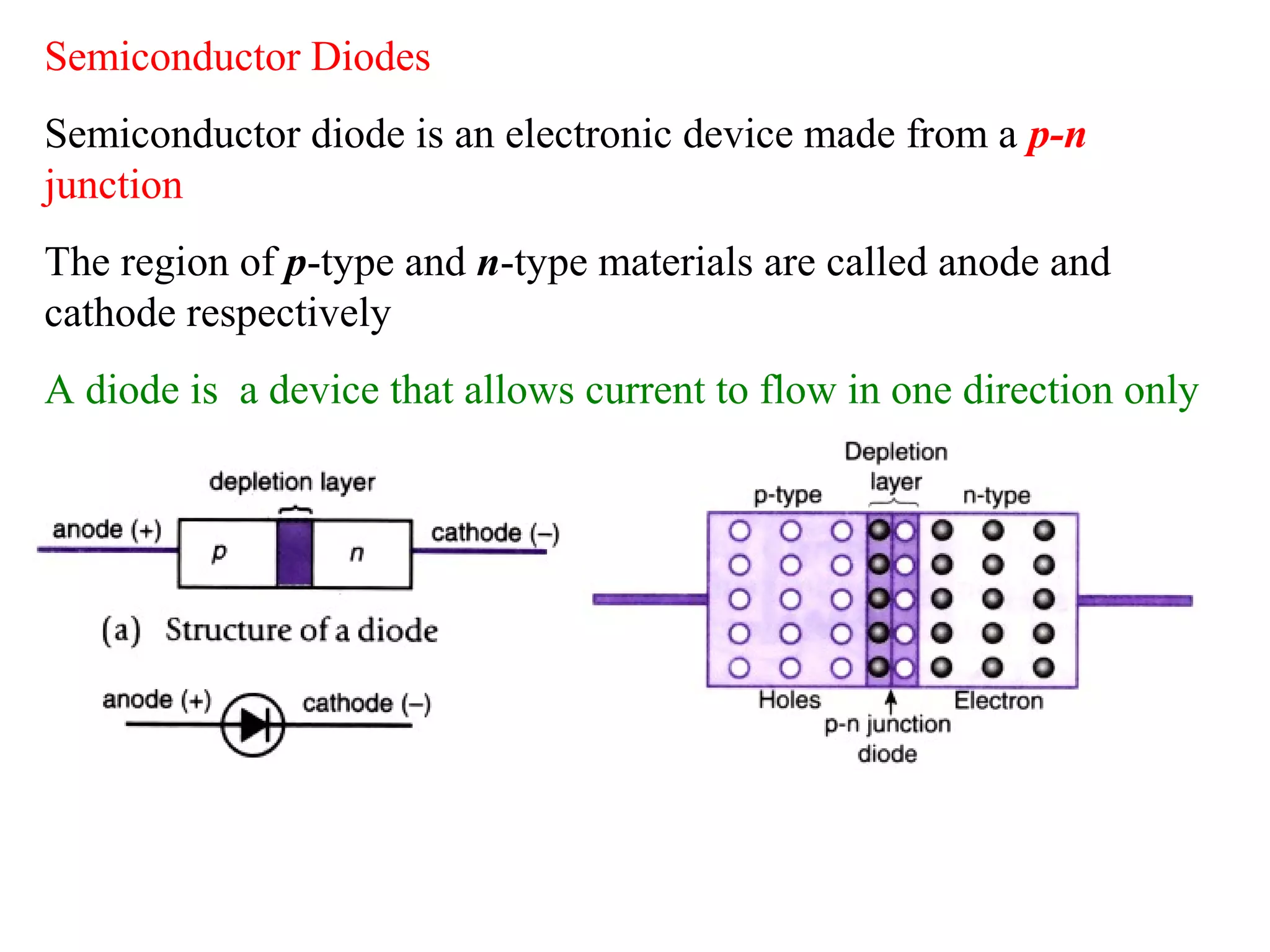
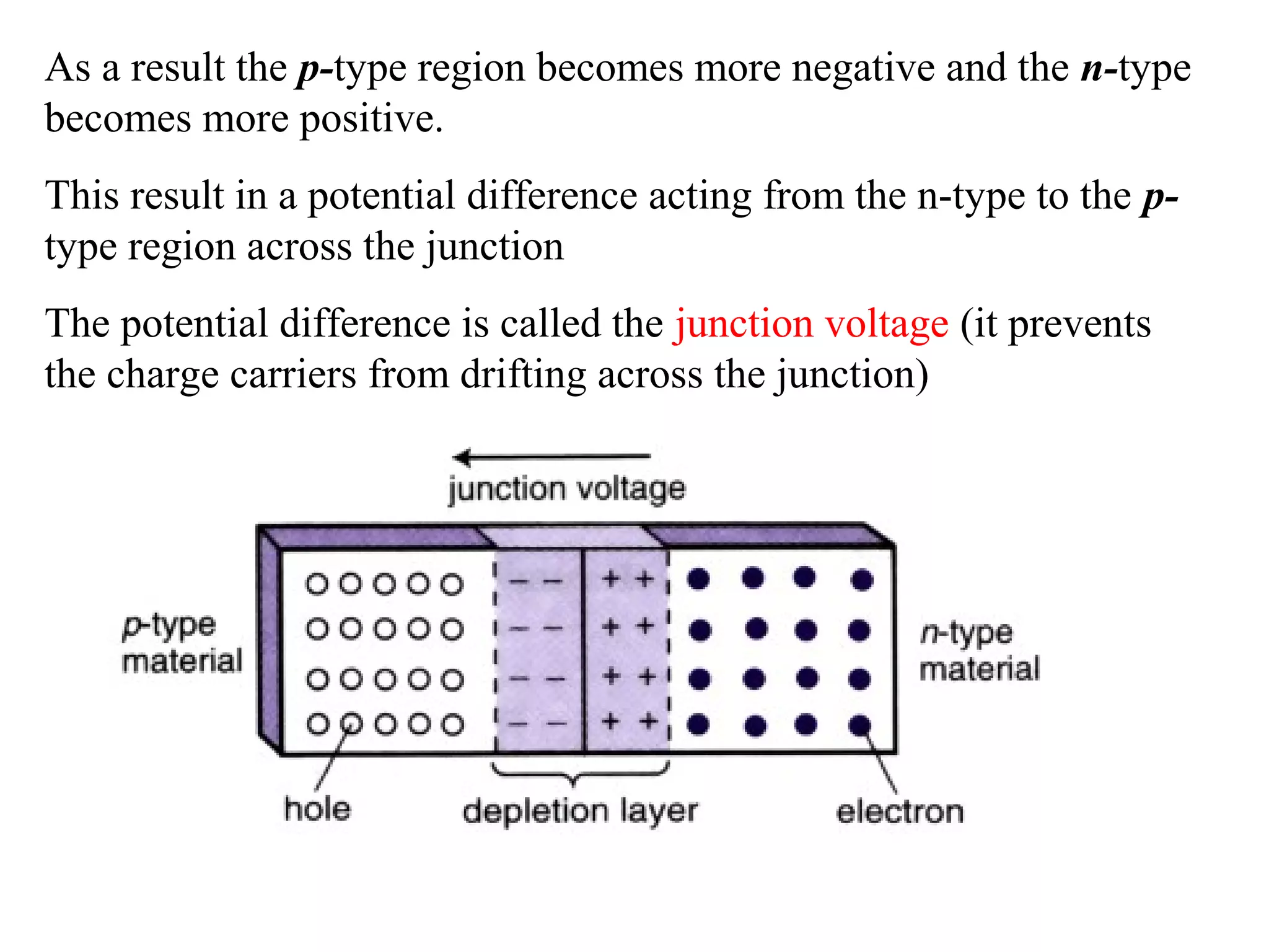
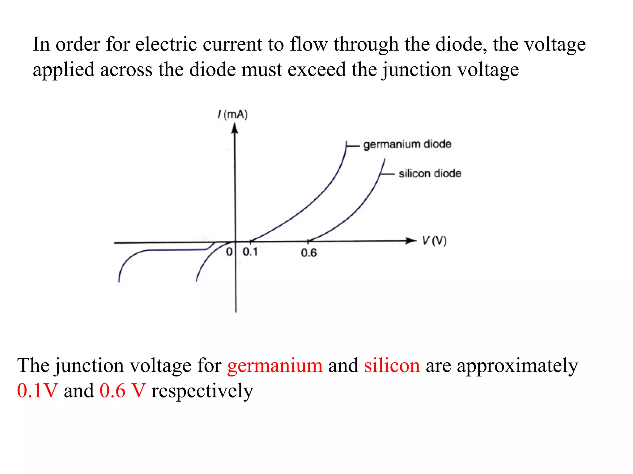
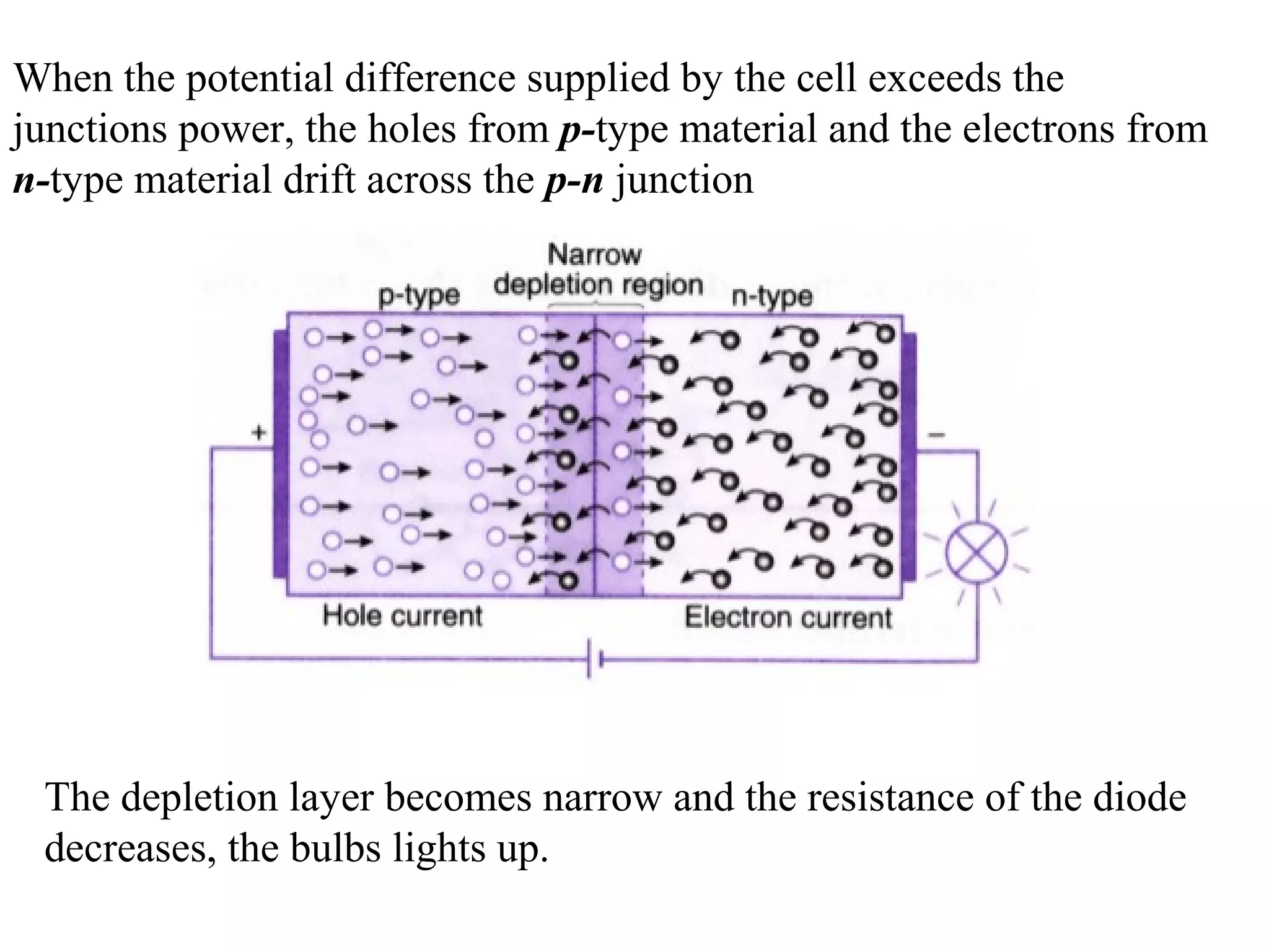
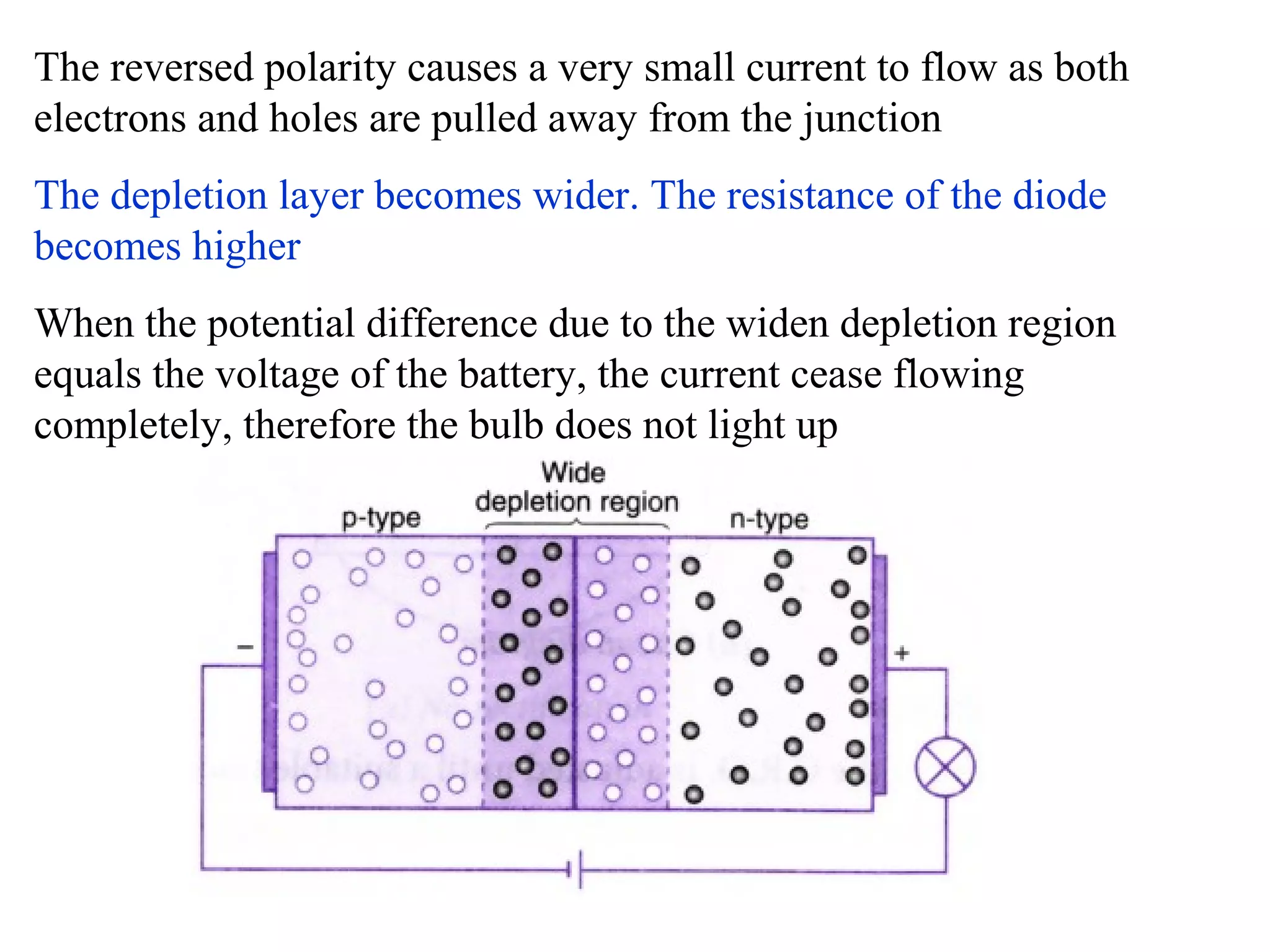
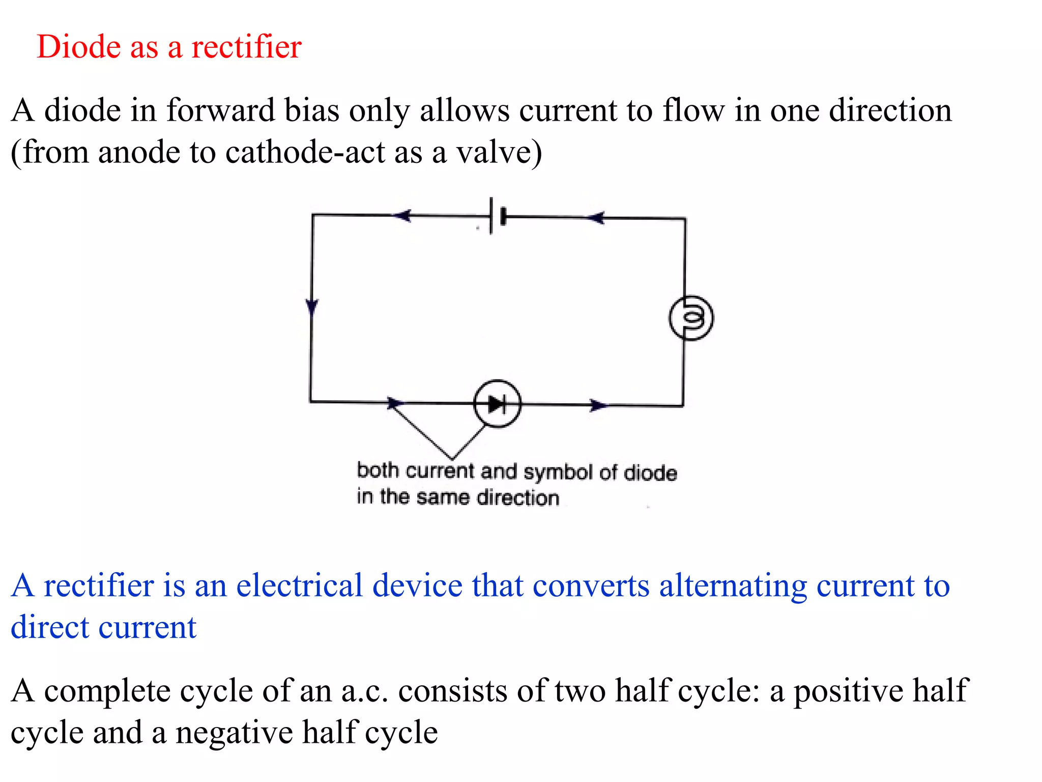
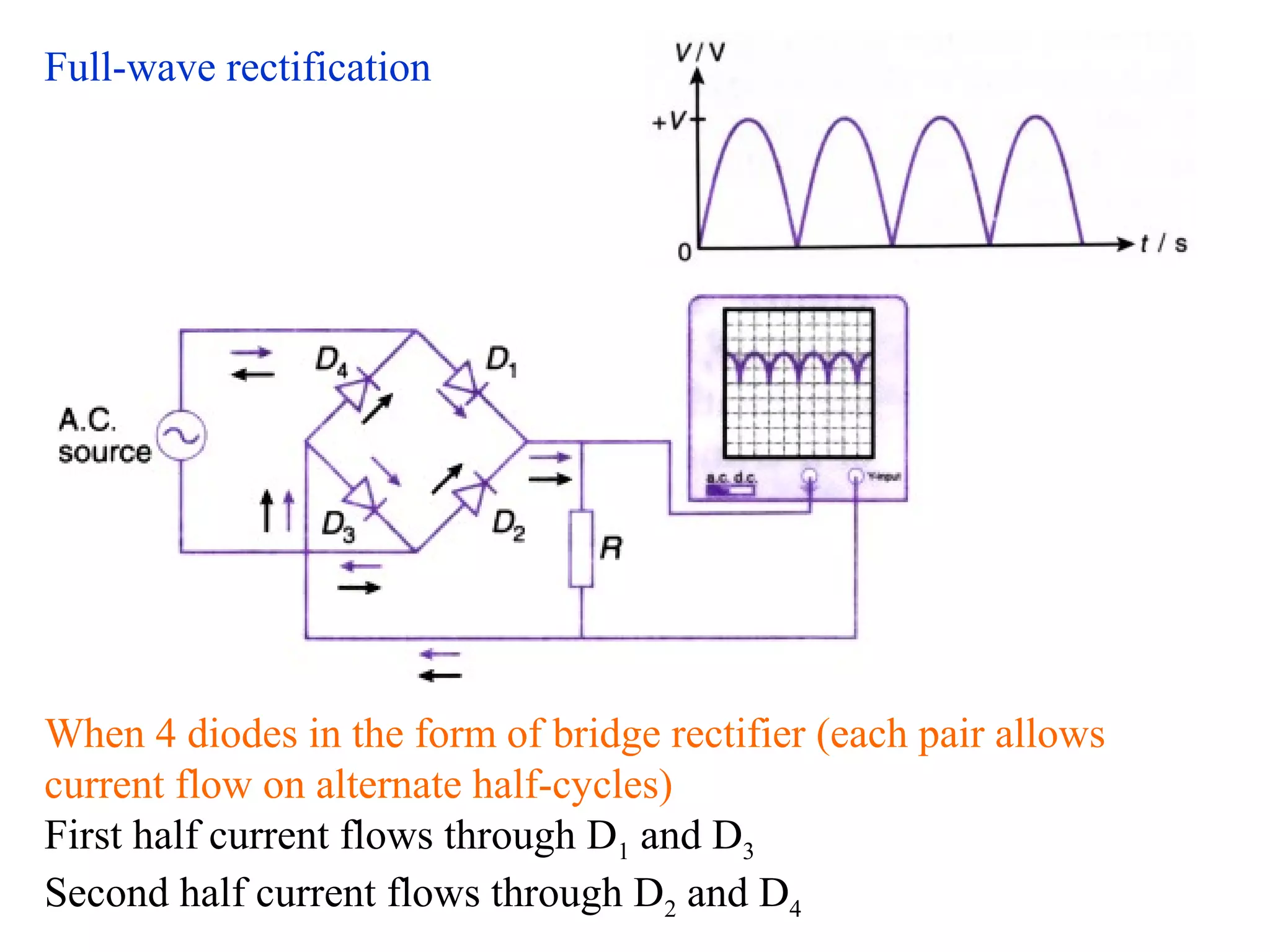
This document discusses semiconductors and semiconductor diodes. It defines semiconductors and describes their properties. It explains how doping semiconductors creates an excess of either electrons or holes, resulting in n-type or p-type materials. It then discusses how a p-n junction diode works, including the formation of a depletion region and the forward and reverse bias connections. The document also covers how diodes can be used for rectification of alternating current into direct current, including half-wave and full-wave rectification, and how a capacitor can smooth the rectified output.
Patrick Henry is at a great position in Entropic Communication As CEO. This company founded in 2001. Entropic Communications is a provider of semiconductor solutions for the connected home.
Introduction
Semiconductor is a solid substance that has conductivity between that of an insulator and that of most metals, either due to the addition of an impurity or because of temperature effects. Devices made of semiconductors, notably silicon, are essential components of most electronic circuits.
Examples: Silicon, Germanium, Carbon
Intrinsic & Extrinsic Semiconductor
Semiconductors are mainly classified into two categories: Intrinsic and Extrinsic. An intrinsic semiconductor material is chemically very pure and possesses poor conductivity. It has equal numbers of negative carriers (electrons) and positive carriers (holes). Where as an extrinsic semiconductor is an improved intrinsic semiconductor with a small amount of impurities added.
The Doping of Semiconductors
The addition of a small percentage of foreign atoms in the regular crystal lattice of silicon or germanium produces dramatic changes in their electrical properties, producing n-type and p-type semiconductors.
Pentavalent impurities
Impurity atoms with 5 valence electrons produce n-type semiconductors by contributing extra electrons.
Trivalent impurities
Impurity atoms with 3 valence electrons produce p-type semiconductors by producing a "hole" or electron deficiency.
N-Type Semiconductor
The addition of pentavalent impurities such as antimony, arsenic or phosphorous contributes free electrons, greatly increasing the conductivity of the intrinsic semiconductor. Phosphorous may be added by diffusion of phosphine gas (PH3).
P-Type Semiconductor
The addition of trivalent impurities such as boron, aluminum or gallium to an intrinsic semiconductor creates deficiencies of valence electrons,called "holes". It is typical to use B2H6 diborane gas to diffuse boron into the silicon material.
Diodes
A device that blocks current in one direction while letting current flow in another direction is called a diode. Diodes can be used in a number of ways. For example, a device that uses batteries often contains a diode that protects the device if you insert the batteries backward. The diode simply blocks any current from leaving the battery if it is reversed -- this protects the sensitive electronics in the device.
Introduction to Semiconductor Devices.
In modern world no other technology permeates every nook and cranny of our existence as does electronics.
Application of electronics are : Televisions, radios, stereo equipment, computers, scanners, electronic control systems (in cars for example) etc.
This ppt is about semiconductor diodes.You can get every basic information about PN junction diode and its working and some more information about the semiconductors.
This presentation gives a lot of information about
Semiconductor Devices.This is presented by Rajesh Kumar Sangani from Rajiv Gandhi University of Knowledge Technologies,Basar Dist
Adilabad,A.P,India.
Outline
Gaya pd muatan bergerak
Gaya pd unsur arus diferensial
Gaya antara unsur arus diferensial
Gaya dan torka
Magnetisasi
Syarat batas magnetik
Rangkaian magnetik
Induktansi & induktansi bersama
Kuliah Medan Elektro magnetik 1. Dasar-dasar dari vektor (Basic of vector).
Meliputi
Skalar dan Vektor
Aljabar dan perkalian vektor (Dot and cross product)
Komponen vektor dan vektor satuan
Contoh soal
Voltage multipliers are AC-to-DC power conversion devices, comprised of diodes and capacitors, that produce a high potential DC voltage from a lower voltage AC source. Multipliers are made up of multiple stages. Each stage is comprised of one diode and one capacitor.
Materi power point adalah sebagai berikut
1. Medan Magnet Konstan
2. Gaya-gaya magnet, Bahan Magnetik, dan Induktansi
3. Medan Fungsi Waktu dan Persamaan-persamaan Maxwell
4. Gelombang Datar Serbasama
Introduction to semiconductor lasers, and its working. construction of semiconductor laser, Ga As laser, and construction, achievement of population inversion, pumping.
Electronics and Communication Engineering is the Branch of Engineering. Electronics and Communication Engineering field requires an understanding of core areas including Engineering Graphics, Computer Programming,Electronics Devices and Circuits-I, Network Analysis, Signals and Systems, Communication Systems, Electromagnetics Engineering, Digital Signal Processing, Embedded Systems, Microprocessor and Computer Architecture. Ekeeda offers Online Mechanical Engineering Courses for all the Subjects as per the Syllabus. Visit : https://ekeeda.com/streamdetails/stream/Electronics-and-Communication-Engineering
Penerangan tentangan aspek-aspek pelaksanaan peperiksaan berpusat amali sains yang akan dilaksanakan dalam SPM 2015. Termasuk contoh arahan persediaan amali untuk penyelia mata pelajaran dan juga contoh soalan untuk calon peperiksaan
A Strategic Approach: GenAI in EducationPeter Windle
Artificial Intelligence (AI) technologies such as Generative AI, Image Generators and Large Language Models have had a dramatic impact on teaching, learning and assessment over the past 18 months. The most immediate threat AI posed was to Academic Integrity with Higher Education Institutes (HEIs) focusing their efforts on combating the use of GenAI in assessment. Guidelines were developed for staff and students, policies put in place too. Innovative educators have forged paths in the use of Generative AI for teaching, learning and assessments leading to pockets of transformation springing up across HEIs, often with little or no top-down guidance, support or direction.
This Gasta posits a strategic approach to integrating AI into HEIs to prepare staff, students and the curriculum for an evolving world and workplace. We will highlight the advantages of working with these technologies beyond the realm of teaching, learning and assessment by considering prompt engineering skills, industry impact, curriculum changes, and the need for staff upskilling. In contrast, not engaging strategically with Generative AI poses risks, including falling behind peers, missed opportunities and failing to ensure our graduates remain employable. The rapid evolution of AI technologies necessitates a proactive and strategic approach if we are to remain relevant.
Safalta Digital marketing institute in Noida, provide complete applications that encompass a huge range of virtual advertising and marketing additives, which includes search engine optimization, virtual communication advertising, pay-per-click on marketing, content material advertising, internet analytics, and greater. These university courses are designed for students who possess a comprehensive understanding of virtual marketing strategies and attributes.Safalta Digital Marketing Institute in Noida is a first choice for young individuals or students who are looking to start their careers in the field of digital advertising. The institute gives specialized courses designed and certification.
for beginners, providing thorough training in areas such as SEO, digital communication marketing, and PPC training in Noida. After finishing the program, students receive the certifications recognised by top different universitie, setting a strong foundation for a successful career in digital marketing.
Unit 8 - Information and Communication Technology (Paper I).pdfThiyagu K
This slides describes the basic concepts of ICT, basics of Email, Emerging Technology and Digital Initiatives in Education. This presentations aligns with the UGC Paper I syllabus.
Acetabularia Information For Class 9 .docxvaibhavrinwa19
Acetabularia acetabulum is a single-celled green alga that in its vegetative state is morphologically differentiated into a basal rhizoid and an axially elongated stalk, which bears whorls of branching hairs. The single diploid nucleus resides in the rhizoid.
Operation “Blue Star” is the only event in the history of Independent India where the state went into war with its own people. Even after about 40 years it is not clear if it was culmination of states anger over people of the region, a political game of power or start of dictatorial chapter in the democratic setup.
The people of Punjab felt alienated from main stream due to denial of their just demands during a long democratic struggle since independence. As it happen all over the word, it led to militant struggle with great loss of lives of military, police and civilian personnel. Killing of Indira Gandhi and massacre of innocent Sikhs in Delhi and other India cities was also associated with this movement.
Macroeconomics- Movie Location
This will be used as part of your Personal Professional Portfolio once graded.
Objective:
Prepare a presentation or a paper using research, basic comparative analysis, data organization and application of economic information. You will make an informed assessment of an economic climate outside of the United States to accomplish an entertainment industry objective.
Model Attribute Check Company Auto PropertyCeline George
In Odoo, the multi-company feature allows you to manage multiple companies within a single Odoo database instance. Each company can have its own configurations while still sharing common resources such as products, customers, and suppliers.
June 3, 2024 Anti-Semitism Letter Sent to MIT President Kornbluth and MIT Cor...Levi Shapiro
Letter from the Congress of the United States regarding Anti-Semitism sent June 3rd to MIT President Sally Kornbluth, MIT Corp Chair, Mark Gorenberg
Dear Dr. Kornbluth and Mr. Gorenberg,
The US House of Representatives is deeply concerned by ongoing and pervasive acts of antisemitic
harassment and intimidation at the Massachusetts Institute of Technology (MIT). Failing to act decisively to ensure a safe learning environment for all students would be a grave dereliction of your responsibilities as President of MIT and Chair of the MIT Corporation.
This Congress will not stand idly by and allow an environment hostile to Jewish students to persist. The House believes that your institution is in violation of Title VI of the Civil Rights Act, and the inability or
unwillingness to rectify this violation through action requires accountability.
Postsecondary education is a unique opportunity for students to learn and have their ideas and beliefs challenged. However, universities receiving hundreds of millions of federal funds annually have denied
students that opportunity and have been hijacked to become venues for the promotion of terrorism, antisemitic harassment and intimidation, unlawful encampments, and in some cases, assaults and riots.
The House of Representatives will not countenance the use of federal funds to indoctrinate students into hateful, antisemitic, anti-American supporters of terrorism. Investigations into campus antisemitism by the Committee on Education and the Workforce and the Committee on Ways and Means have been expanded into a Congress-wide probe across all relevant jurisdictions to address this national crisis. The undersigned Committees will conduct oversight into the use of federal funds at MIT and its learning environment under authorities granted to each Committee.
• The Committee on Education and the Workforce has been investigating your institution since December 7, 2023. The Committee has broad jurisdiction over postsecondary education, including its compliance with Title VI of the Civil Rights Act, campus safety concerns over disruptions to the learning environment, and the awarding of federal student aid under the Higher Education Act.
• The Committee on Oversight and Accountability is investigating the sources of funding and other support flowing to groups espousing pro-Hamas propaganda and engaged in antisemitic harassment and intimidation of students. The Committee on Oversight and Accountability is the principal oversight committee of the US House of Representatives and has broad authority to investigate “any matter” at “any time” under House Rule X.
• The Committee on Ways and Means has been investigating several universities since November 15, 2023, when the Committee held a hearing entitled From Ivory Towers to Dark Corners: Investigating the Nexus Between Antisemitism, Tax-Exempt Universities, and Terror Financing. The Committee followed the hearing with letters to those institutions on January 10, 202
2024.06.01 Introducing a competency framework for languag learning materials ...Sandy Millin
http://sandymillin.wordpress.com/iateflwebinar2024
Published classroom materials form the basis of syllabuses, drive teacher professional development, and have a potentially huge influence on learners, teachers and education systems. All teachers also create their own materials, whether a few sentences on a blackboard, a highly-structured fully-realised online course, or anything in between. Despite this, the knowledge and skills needed to create effective language learning materials are rarely part of teacher training, and are mostly learnt by trial and error.
Knowledge and skills frameworks, generally called competency frameworks, for ELT teachers, trainers and managers have existed for a few years now. However, until I created one for my MA dissertation, there wasn’t one drawing together what we need to know and do to be able to effectively produce language learning materials.
This webinar will introduce you to my framework, highlighting the key competencies I identified from my research. It will also show how anybody involved in language teaching (any language, not just English!), teacher training, managing schools or developing language learning materials can benefit from using the framework.
2024.06.01 Introducing a competency framework for languag learning materials ...
Understanding semiconductor diodes
1. Understanding Semiconductor Diodes
Properties of Semiconductor
Semiconductor : Material whose conductivity is between conductor and
insulator
Semiconductor behaves as an insulator at very low temperature with
appreciable electrical conductivity at room temperature but good
conductor at high temperature
2. Pure Element Semiconductors: Silicon, germanium, boron,
tellurium and selenium
Compound Semiconductors: Lead sulphide, gallium arsenide,
cadmium selenide and indium arsenide
A silicon atom
3. Typical semiconductor materials are silicon and germanium. Each
has 4 electrons in its outer orbital (outermost shell)
Each electron in the outer orbital can form a covalent bond with one
electron from outer orbital of another atom (Form four covalent
bonds with four neighbouring atoms)
When at high temperature, the thermal energy of the vibrating atoms
causes some electrons to break free
4. For every electron that is broken free, there is a hole in the
bonding structure. The atom is neutral, it has a complete set of
protons and electrons, the hole behaves as if it has a positive
charge.
5. Two types of charge carriers in a semiconductor: the electron and hole
When electron is removed from a covalent bond, it leaves a vacancy
(hole). An electron from a neighbouring atom can fill this vacancy,
leaving neighbouring atom now with a vacancy. Therefore the
vacancy (hole) can travel through the lattice and act as a charge carrier.
6. Doping of Semiconductor
Doping: Process of adding a certain amount of specific impurities
(dopants) to a crystalline lattice of semiconductor, to increase the
conductivity.
Type of semiconductors produced by doping: p-type semiconductor
and n-type semiconductor
p-type
semiconductor
7. p-type doping (Create an abundance of holes in the material)
By doping trivalent atoms such as boron, gallium or aluminium to
replace some of the silicon atoms.
One electron is missing from one of the four covalent bond
The trivalent atoms are called acceptor atoms, because they accept
any free electrons to fill the holes. When accepting an electron
from its neighbouring atom, a hole is created due to deficiency of
electron.
If more trivalent atoms are added, there will be more holes than
free electrons, hence holes are now majority carriers and free
electrons are the minority carriers
8. n-type semiconductor (Produce abundance of electrons)
By doping pentavalent atoms such as phosphorus, arsenic or antimony
to replace some of the silicon atoms.
Each of the pentavalent atoms will have four covalent bonds and one
extra electron. A free electron is available as a charge carrier
The pentavalent atom donates an extra electron it is therefore called the
donor atom.
The free electrons are the majority charge carriers and the holes are the
minority charge carriers.
n-type
semiconductor
9. Semiconductor Diodes
Semiconductor diode is an electronic device made from a p-n
junction
The region of p-type and n-type materials are called anode and
cathode respectively
A diode is a device that allows current to flow in one direction only
10. The depletion layer is formed when there is a decrease in the free
electrons and holes in the region around the p-n junction.
The electrons from the n-type material drift across the junction to fill
in the holes in the p-type material. The holes from the p-type material
drift in the opposite direction
depletion layer
11. As a result the p-type region becomes more negative and the n-type
becomes more positive.
This result in a potential difference acting from the n-type to the p-
type region across the junction
The potential difference is called the junction voltage (it prevents
the charge carriers from drifting across the junction)
12. In order for electric current to flow through the diode, the voltage
applied across the diode must exceed the junction voltage
The junction voltage for germanium and silicon are approximately
0.1V and 0.6 V respectively
13. Ways of connection of diodes
Forward bias connection
The p-type (anode) is connected to the positive terminal and the n-
type (cathode) is connected to the negative terminal
14. When the potential difference supplied by the cell exceeds the
junctions power, the holes from p-type material and the electrons from
n-type material drift across the p-n junction
The depletion layer becomes narrow and the resistance of the diode
decreases, the bulbs lights up.
15. Reverse bias
The n-type is connected to the positive terminal and the p-type is
connected to the negative terminal
16. The reversed polarity causes a very small current to flow as both
electrons and holes are pulled away from the junction
The depletion layer becomes wider. The resistance of the diode
becomes higher
When the potential difference due to the widen depletion region
equals the voltage of the battery, the current cease flowing
completely, therefore the bulb does not light up
17. Diode as a rectifier
A diode in forward bias only allows current to flow in one direction
(from anode to cathode-act as a valve)
A rectifier is an electrical device that converts alternating current to
direct current
A complete cycle of an a.c. consists of two half cycle: a positive half
cycle and a negative half cycle
18.
19. Two type of rectification:
a) Half-wave rectification
b) Full-wave rectification
Half-wave rectification
The current will only flow in the first half-cycle when the diode is
forward bias and is blocked in the second half, when the diode is in
reverse bias.
Current flowing is half-wave rectified
20. Full-wave rectification
When 4 diodes in the form of bridge rectifier (each pair allows
current flow on alternate half-cycles)
First half current flows through D1 and D3
Second half current flows through D2 and D4
21. Full-wave rectification is a process where both halves of every cycle
of an alternating current is made to flow in the same direction
Capacitor Smoothing
Both half-wave and full-wave rectification do not provide a steady
direct current like battery.
A capacitor is used to smoothen the rectified output
capacitor
22. During the forward peaks (positive half-cycles), the capacitor is
charged up. Energy is stored in the capacitor.
In between the forward peaks (negative half-cycles), the capacitor
releases its charge (discharges). It acts as an reservoir and maintain
the p.d. across the load
24. The circuit in the figure below is a full-wave rectifier
a). Draw the symbol of diodes in the figure so that the current flow in
the direction indicated by the arrow
b). Draw the graph to show the effect of these diodes on the alternating
current
c). If a capacitor is connected across R, what is the effect on the
alternating current?
d). Is it possible to turn alternating current below into a constant direct
25. Current using a capacitor as shown below? Explain how this can be
done
Answer:
a).
b).
c). The alternating current will be “smoothed”.
d). Yes. By using a capacitor with higher capacitance.