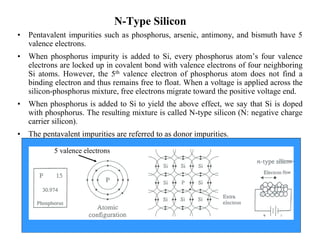
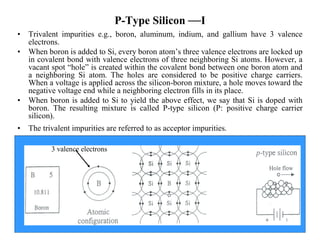
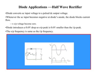
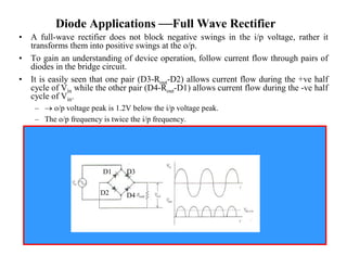
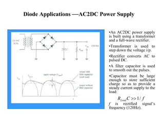
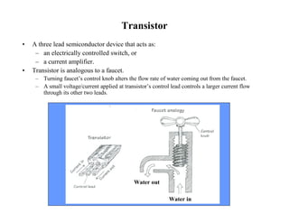
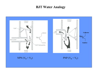
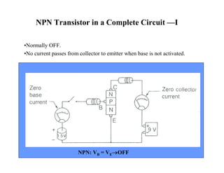
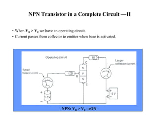
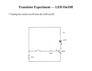
SlideShare a Scribd company logo
Basic Electronics
Semiconductor —I 
• Materials that permit flow of electrons are called 
conductors (e.g., gold, silver, copper, etc.). 
• Materials that block flow of electrons are called 
insulators (e.g., rubber, glass, Teflon, mica, etc.). 
• Materials whose conductivity falls between those 
of conductors and insulators are called 
semiconductors. 
• Semiconductors are “part-time” conductors 
whose conductivity can be controlled. 
germanium 
Semiconductors 
silicon
Semiconductor —II 
• Silicon is the most common material used to build semiconductor devices. 
• Si is the main ingredient of sand and it is estimated that a cubic mile of seawater 
contains 15,000 tons of Si. 
• Si is spun and grown into a crystalline structure and cut into wafers to make 
electronic devices.
Semiconductor —III 
• Atoms in a pure silicon wafer contains four electrons in outer orbit (called valence 
electrons). 
– Germanium is another semiconductor material with four valence electrons. 
• In the crystalline lattice structure of Si, the valence electrons of every Si atom are 
locked up in covalent bonds with the valence electrons of four neighboring Si atoms. 
– In pure form, Si wafer does not contain any free charge carriers. 
– An applied voltage across pure Si wafer does not yield electron flow through the wafer. 
– A pure Si wafer is said to act as an insulator. 
• In order to make useful semiconductor devices, materials such as phosphorus (P) and 
boron (B) are added to Si to change Si’s conductivity. 
4 valence electrons
N-Type Silicon 
• Pentavalent impurities such as phosphorus, arsenic, antimony, and bismuth have 5 
valence electrons. 
• When phosphorus impurity is added to Si, every phosphorus atom’s four valence 
electrons are locked up in covalent bond with valence electrons of four neighboring 
Si atoms. However, the 5th valence electron of phosphorus atom does not find a 
binding electron and thus remains free to float. When a voltage is applied across the 
silicon-phosphorus mixture, free electrons migrate toward the positive voltage end. 
• When phosphorus is added to Si to yield the above effect, we say that Si is doped 
with phosphorus. The resulting mixture is called N-type silicon (N: negative charge 
carrier silicon). 
• The pentavalent impurities are referred to as donor impurities. 
5 valence electrons
P-Type Silicon —I 
• Trivalent impurities e.g., boron, aluminum, indium, and gallium have 3 valence 
electrons. 
• When boron is added to Si, every boron atom’s three valence electrons are locked up 
in covalent bond with valence electrons of three neighboring Si atoms. However, a 
vacant spot “hole” is created within the covalent bond between one boron atom and 
a neighboring Si atom. The holes are considered to be positive charge carriers. 
When a voltage is applied across the silicon-boron mixture, a hole moves toward the 
negative voltage end while a neighboring electron fills in its place. 
• When boron is added to Si to yield the above effect, we say that Si is doped with 
boron. The resulting mixture is called P-type silicon (P: positive charge carrier 
silicon). 
• The trivalent impurities are referred to as acceptor impurities. 
3 valence electrons
P-Type Silicon —II 
• The hole of boron atom points towards the negative terminal. 
• The electron of neighboring silicon atom points toward 
positive terminal. 
• The electron from neighboring silicon atom falls into the 
boron atom filling the hole in boron atom and creating a “new” 
hole in the silicon atom. 
• It appears as though a hole moves toward the negative 
terminal!
Diode 
•A diode is a 2 lead semiconductor that acts as a one way gate to electron flow. 
– Diode allows current to pass in only one direction. 
•A pn-junction diode is formed by joining together n-type and p-type silicon. 
•In practice, as the n-type Si crystal is being grown, the process is abruptly altered to 
grow p-type Si crystal. Finally, a glass or plastic coating is placed around the joined 
crystal. 
•The p-side is called anode and the n-side is called cathode. 
•When the anode and cathode of a pn-junction diode are connected to external voltage 
such that the potential at anode is higher than the potential at cathode, the diode is said 
to be forward biased. 
–In a forward-biased diode current is allowed to flow through the device. 
•When potential at anode is smaller than the potential at cathode, the diode is said to 
be reverse biased. In a reverse-biased diode current is blocked. 
+ - + -
Water Analogy of Diodes 
• When water pressure on left overcomes the restoring force of spring, the gate is 
opened and water is allowed to flow . 
• When water pressure is from right to left, the gate is pressed against the solid stop 
and no water is allowed to flow. 
• Spring restoring force is analogous to 0.6V needed to forward bias a Si diode.
Diode: How it Works —I 
• When a diode is 
connected to a battery as 
shown, electrons from 
the n-side and holes from 
the p-side are forced 
toward the center by the 
electrical field supplied 
by the battery. The 
electrons and holes 
combine causing the 
current to pass through 
the diode. When a diode 
is arranged in this way, it 
is said to be forward-biased. 
Repels holes 
Repels electrons 
Forward-biased (“open door”)
Diode: How it Works—II 
• A diode’s one-way gate feature does not work all the time. 
• Typically for silicon diodes, an applied voltage of 0.6V or greater is needed, 
otherwise, the diode will not conduct. 
• This feature is useful in forming a voltage-sensitive switch. 
• I-V characteristics for silicon and germanium diodes is shown below.
Diode: How it doesn’t work 
• When a diode is 
connected to a battery as 
shown, holes in the n-side 
are forced to the 
left while electrons in 
the p-side are forced to 
the right. This results in 
an empty zone around 
the pn- junction that is 
free of charge carries 
creating a depletion 
region. This depletion 
region acts as an 
insulator preventing 
current from flowing 
through the diode. 
When a diode is 
arranged in this way, it 
is said to be reverse-biased. 
Attracts holes Attracts electrons 
Reverse-biased (“closed door”)
Diode Applications —Half Wave Rectifier 
•Diode converts ac input voltage to a pulsed dc output voltage. 
•Whenever the ac input becomes negative at diode’s anode, the diode blocks current 
flow. 
– o/p voltage become zero. 
•Diode introduces a 0.6V drop so o/p peak is 0.6V smaller than the i/p peak. 
•The o/p frequency is same as the i/p frequency. 
Vin
Diode Applications —Full Wave Rectifier 
• A full-wave rectifier does not block negative swings in the i/p voltage, rather it 
transforms them into positive swings at the o/p. 
• To gain an understanding of device operation, follow current flow through pairs of 
diodes in the bridge circuit. 
• It is easily seen that one pair (D3-Rout-D2) allows current flow during the +ve half 
cycle of Vin while the other pair (D4-Rout-D1) allows current flow during the -ve half 
cycle of Vin. 
–  o/p voltage peak is 1.2V below the i/p voltage peak. 
– The o/p frequency is twice the i/p frequency. 
D1 D3 
D2 D4
Diode Applications —AC2DC Power Supply 
•An AC2DC power supply 
is built using a transformer 
and a full-wave rectifier. 
•Transformer is used to 
step down the voltage i/p. 
•Rectifier converts AC to 
pulsed DC. 
•A filter capacitor is used 
to smooth out the pulses. 
•Capacitor must be large 
enough to store sufficient 
charge so as to provide a 
steady current supply to the 
load: 
RLoadC 1/ f 
f is rectified signal’s 
frequency (120Hz).
Transistor 
• A three lead semiconductor device that acts as: 
– an electrically controlled switch, or 
– a current amplifier. 
• Transistor is analogous to a faucet. 
– Turning faucet’s control knob alters the flow rate of water coming out from the faucet. 
– A small voltage/current applied at transistor’s control lead controls a larger current flow 
through its other two leads. 
Water in 
Water out
Transistor Types: BJT, JFET, and MOSFET 
• Bipolar Junction Transistor (BJT) 
– NPN and PNP 
• Junction Field Effect Transistor (JFET) 
– N-channel and P-channel 
• Metal Oxide Semiconductor FET (MOSFET) 
– Depletion type (n- and p-channel) and enhancement type (n- and p-channel) 
BJT JFET MOSFET
BJT Types 
• NPN and PNP. 
– NPN: a small input current and a positive voltage applied @ its base (with VB>VE) 
allows a large current to flow from collector to emitter. 
– PNP: a small output current and a negative voltage @ its base (with VB<VE) allows a 
much larger current to flow from emitter to collector.
NPN BJT: How it works —I 
• When no voltage is applied at 
transistor’s base, electrons in the 
emitter are prevented from passing 
to the collector side because of the 
pn junction. 
• If a negative voltage is applied to 
the base, things get even worse as 
the pn junction between the base 
and emitter becomes reverse-biased 
resulting in the formation of 
a depletion region that prevents 
current flow.
NPN BJT: How it works —II 
• If a positive voltage (>0.6V) is 
applied to the base of an npn 
transistor, the pn junction between 
the base and emitter becomes 
forward-biased. During forward 
bias, escaping electrons are drawn 
to the positive base. 
• Some electrons exit through the 
base, but because the p-type base 
is so thin, the onslaught of 
electrons that leave the emitter get 
close enough to the collector side 
that they begin jumping into the 
collector. Increasing the base 
voltage increases the emitter-to-collector 
electron flow. 
• Recall, positive current flow is in 
the direction opposite to the 
electron flow current flows from 
collector to emitter.
BJT Water Analogy 
NPN (VB > VE) PNP (VB < VE) 
Base 
Collector 
Emitter
NPN Transistor in a Complete Circuit —I 
•Normally OFF. 
•No current passes from collector to emitter when base is not activated. 
NPN: VB = VEOFF
NPN Transistor in a Complete Circuit —II 
• When VB > VE we have an operating circuit. 
• Current passes from collector to emitter when base is activated. 
NPN: VB > VE ON
Transistor Experiment —LED On/Off 
• Turning the switch on/off turns the LED on/off.
JFET 
• Junction field effect transistors like BJTs are three lead 
semiconductor devices. 
• JFETs are used as: 
– electrically controlled switches, 
– current amplifiers, and 
– voltage-controlled resistors. 
• Unlike BJTs, JFETs do not require a bias current and are controlled 
by using only a voltage. 
• JFETs are normally on when VG - VS = 0. 
• When VG - VS  0, then JFETs become resistive to current flow 
through the drain-source pair  “JFETs are depletion devices.”
JFET Types 
• Two types of JFETs: 
– n-channel and p-channel. 
• In n-channel JFET, a –ve voltage applied @ its gate (with VG < VS) reduces current 
flow from drain to source. It operates with VD > VS. 
• In p-channel JFET, a +ve voltage applied @ its gate (with VG > VS) reduces current 
flow from source to drain. It operates with VS > VD. 
• JFETs have very high input impedance and draw little or no input current 
–  if there is any circuit/component connected to the gate of a JFET, no current is drawn 
away from or sunk into this circuit.
MOSFET 
• Metal oxide semiconductor FET. 
• Similar to JFET. 
• A metal oxide insulator is placed @ the gate to obtain a high input impedance @ the 
gate 
– gate input impedance approx. 1014Ω. 
• Use of insulator as described above yields a low gate-to-channel capacitance. 
– If too much static electricity builds up on the gate, then the MOSFET may be damaged.
MOSFET Types 
• Enhancement type: 
– Normally off, thus no current flows through drain-source channel when VG = VS. 
– When a voltage applied @ the gate causes VG  VS the drain-source channel reduces 
resistance to current flow. 
• Depletion type: 
– Normally on, thus maximum current flows through drain-source channel when VG = VS. 
– When a voltage applied @ the gate causes VG  VS the drain-source channel increases 
resistance to current flow. 
Current flow increases with: Current flow decreases with: 
VG > VS VG < VS VG < VS VG > VS
Optoelectronics 
• In optoelectronics we deal with 2 types of electronic devices. 
• Light emitting electronic devices: ones that generate electromagnetic energy under 
the action of electrical field. Example: light emitting diodes (visible and infrared 
light). 
• Light detecting devices: ones that transform electromagnetic energy input into 
electrical current/voltage. Examples: photoresistors, photodiodes, phototransistors, 
etc. 
Light emitting diodes Infrared detector
Light-Emitting Diodes (LEDs)
LED 101—I 
• 2 lead semiconductor device. 
• Light emitting PN-junction diode. 
– Visible or infrared light. 
• Has polarity. 
• Recall diodes act as a one way gate to current flow. 
– A forward-biased PN-junction diode allows current flow from anode to cathode. 
• An LED conducts and emits light when its anode is made more positive (approx. 
1.4V) than its cathode. 
– With reverse polarity, LED stops conducting and emitting light.
LED 101—II 
• Similar to diodes, LEDs are current-dependent devices. 
– LED brightness is controlled by controlling current through LED. 
• Too little current through LED  LED remains OFF. 
• Small current through LED  dimly lit LED. 
• Large current through LED  brightly lit LED. 
• Too much current through LED  LED is destroyed. 
• A resistor placed in series with LED accomplishes current control 
+ 
Anode 
- 
Cathode 
LED symbol
LED 101—III 
• Let Vs be the supply voltage. 
• Let Vf be the required forward bias voltage for the 
LED. 
• Let I be the desired current flow through LED. 
• Then, the current limiting resistance R is sized as 
follow: 
V  V  
V 
R 
 V V  
V  
• If R is chosen smaller than the above value, a 
larger current will flow through the LED. 
– LEDs can handle only limited current (varies from 
20mA to 100mA). 
– If current through LED is larger than the maximum 
allowed value, than the LED will be damaged. 
Vs 
I VR 
Vf 
R 
R s f 
R s f 
I I
Visible-Light LED 
• Inexpensive and durable. 
• Typical usage: as indicator lights. 
• Common colors: green (~565nm), yellow (~585nm), orange (~615nm), and red 
(~650nm). 
• Maximum forward voltage:  1.8V. 
• Typical operating currents: 1 to 3mA. 
• Typical brightness levels: 1.0 to 3.0mcd/1mA to 3.0mcd /2mA. 
• High-brightness LEDs exist. 
– Used in high-brightness flashers (e.g., bicycle flashers).
Blinking LED 
• Contain a miniature integrated circuit that causes LED to flash from 1 to 6 times/second. 
• Typical usage: indicator flashers. May also be used as simple oscillators.
Tricolor LED 
• Two LEDs placed in parallel facing opposite directions. 
• One LED is red or orange, the other is green. 
• Current flow in one direction turns one LED ON while the other remains OFF due 
to reverse bias. 
• Current flow in the other direction turns the first LED OFF and the second LED ON. 
• Rapid switching of current flow direction will alternatively turn the two LEDs ON 
giving yellow light. 
• Used as a polarity indicator. 
• Maximum voltage rating: 3V 
• Operating range: 10 to 20mA
7-Segment LED Display 
• Used for displaying numbers and other characters. 
• 7 individual LEDs are used to make up the display. 
• When a voltage is applied across one of the LEDs, a portion of the 8 lights up. 
• Unlike liquid crystal displays (LCD), 7-segment LED displays tend to be more 
rugged, but they also consume more power.
How LED Works 
• The light-emitting section of an LED is made by joining n-type and p-type semiconductors 
together to form a pn junction. 
• When the pn junction is forward-biased, electrons in the n side are excited across the pn 
junction and into the p side, where they combine with holes. 
• As the electrons combine with the holes, photons are emitted. 
• The pn-junction section of an LED is encased in an epoxy shell that is doped with light 
scattering particles to diffuse light and make the LED appear brighter. 
• Often a reflector placed beneath the semiconductor is used to direct the light upward.
Photoresistors—I 
• Light sensitive variable resistors. 
• Its resistance depends on the intensity of light incident upon it. 
– Under dark condition, resistance is quite high (M: called dark resistance). 
– Under bright condition, resistance is lowered (few hundred ). 
• Response time: 
– When a photoresistor is exposed to light, it takes a few milliseconds, before it 
lowers its resistance. 
– When a photoresistor experiences removal of light, it may take a few seconds 
to return to its dark resistance. 
Symbol
Photoresistors—II 
• Some photoresistors respond better to light that contains 
photons within a particular wavelength of spectrum. 
– Example: Cadmium-sulfide photoresistos respond to 
light within 400-800nm range. 
– Example: Lead-sulfide photoresistos respond to infrared 
light.
How PhotoresistorWorks 
• Special semiconductor crystal, such as cadmium sulfide or lead sulfide is used to make 
photoresistors. 
• When this semiconductor is placed in dark, electrons within its structure resist flow through 
the resistor because they are too strongly bound to the crystal’s atoms. 
• When this semiconductor is illuminated, incoming photons of light collide with the bound 
electrons, stripping them from the binding atom, thus creating holes in the process. 
• Liberated electrons contribute to the current flowing through the device.
Photoresistor Application —Light Activated Relay 
• Light-sensitive voltage divider is being 
used to trip a relay whenever the light 
intensity change. 
• Light-activated circuit: 
– When the photoresistor is exposed to 
light, its resistance decreases. 
–  Transistor’s base current and 
voltage increase and if the base current 
and voltage are large enough, the 
collector-emitter pair of the transistor 
conducts triggering the relay. 
• The value of R1 in the light-activated 
circuit should be around 1 KΩ but 
may have to be adjusted. 
• Dark-activated relay works in a similar 
but opposite manner. 
• R1 in the dark-activated circuit 
(100KΩ) may also have to be adjusted. 
• A 6 to 9-V relay with a 500Ω coil can 
be used in either circuit. 
Light activated relay Dark activated relay
Photodiode 
• Photodiode is a 2 lead semiconductor device that transforms light energy to electric 
current. 
• Suppose anode and cathode of a photodiode are wired to a current meter. 
– When photodiode is placed in dark, the current meter displays zero current flow. 
– When the photodiode is expose to light, it acts a a current source, causing current flow 
from cathode to anode of photodiode through the current meter. 
• Photodiodes have very linear light v/s current characteristics. 
– Commonly used as light meters in cameras. 
• Photodiodes often have built-in lenses and optical filters. 
• Response time of a photodiode slows with increasing surface area. 
• Photodiodes are more sensitive than photoresistor. 
Symbol
How Photodiode Works 
• Photodiode: A thin n-type 
semiconductor sandwiched with a 
thicker p-type semiconductor. 
• N-side is cathode, p-side is anode. 
• Upon illumination, a # of photons pass 
from the n-side and into the p-side of 
photodiode. 
– Some photons making it into p-side 
collide with bound electrons within p-semiconductor, 
ejecting them and 
creating holes. 
– If these collisions are close to the pn-interface, 
the ejected electrons cross the 
junction, yielding extra electrons on the 
n-side and extra holes on the p-side. 
– Segregation of +ve and -ve charges 
leads to a potential difference across the 
pn-junction. 
– When a wire is connected between the 
cathode and anode, a conventionally 
positive current flow from the anode to 
cathode
Photodiode Applications—Photovoltaic Current Source 
• Photodiode converts light energy directly into electric current that can be 
measured with meter. 
• The input intensity of light and the output current are nearly linear.
• Solar cells are photodiodes with very large surface areas. 
• Compared to usual photodiodes, the large surface area in photodiode of a 
solar cell yields 
– a device that is more sensitive to incoming light. 
– a device that yields more power (larger current/volts). 
• Solar cells yield more power. 
• A single solar cell may provide up to 0.5V that can supply 0.1A when 
exposed to bright light. 
Solar Cell—I
Solar Cell—II
Solar Cell Basic Operation—Power Sources 
• Each solar cell produces an 
open-circuit voltage from 
around 0.45 to 0.5 V and may 
generate as much as 0.1 A in 
bright light. 
• Similar to batteries, solar cells 
can be combined in series or 
parallel. 
• Adding cells in series, yields 
output voltage that is the sum 
of the individual cell voltages. 
• Adding solar cells in parallel, 
yields an increased output 
current vis-à-vis a single solar 
cell.
Solar Cell Basic Operation—Battery Charger 
• Nine solar cells placed in series can 
be used to recharge two 1.5 V NiCd 
cells. 
• The diode is added to the circuit to 
prevent the NiCd cells from 
discharging through the solar cell 
during times of darkness. 
• It is important not to exceed the safe 
charging rate of NiCd cells. To slow 
the charge rate, a resistor can be 
placed in series with the batteries.
Phototransistor 
• Phototransistor is a light sensitive transistor. 
• In one common type of phototransistor, the base lead of a BJT is replaced by a light 
sensitive surface. 
• When the light sensitive surface @ the base is kept in darkness, the collector-emitter 
pair of the BJT does not conduct. 
• When the light sensitive surface @ the base is exposed to light, a small amount of 
current flows from the base to the emitter. The small base-emitter current controls 
the larger collector-emitter current. 
• Alternatively, one can also use a field-effect phototransistor (Photo FET). 
• In a photo FET, the light exposure generates a gate voltage which controls a 
drain-source current. 
Phototransistor Photo FET
How Phototransistor Works 
• The bipolar phototransistor resembles a 
bipolar transistor that has extra large p-type 
semiconductor region that is open for light 
exposure. 
• When photons from a light source collide 
with electrons within the p-type 
semiconductor, they gain enough energy to 
jump across the pn-junction energy barrier-provided 
the photons are of the right 
frequency/energy. 
• As electrons jump from the p-region into the 
lower n-region, holes are created in the p-type 
semiconductor. 
• The extra electrons injected into the lower n-type 
slab are drawn toward the positive 
terminal of the battery, while electrons from 
the negative terminal of the battery are draw 
into the upper n-type semiconductor and 
across the np junction, where they combine 
with the holes, the net result is an electrons 
current that flows from the emitter to the 
collector.
Phototransistor Applications—Light Activated Relay 
• A phototransistor is used to control the base current supplied to a power-switching 
transistor that is used to supply current to a relay. 
• When light comes in contact with the phototransistor, the phototransistor turns on, 
allowing current to pass from the supply into the base of the power-switching 
transistor. 
• This allows the power-switching transistor to turns on, and current flows through the 
relay, triggering it to switch states. 
• The 100K pot is used to adjust the sensitivity of device by controlling current flow 
through the phototransistor.
Phototransistor Applications—Dark Activated Relay 
• A phototransistor is used to control the base current supplied to a power-switching 
transistor that is used to supply current to a relay. 
• When light is removed from the phototransistor, the phototransistor turns off, 
allowing more current to enter into the base of the power-switching transistor. 
• This allows the power-switching transistor to turns on, and current flows through 
the relay, triggering it to switch states. 
• The 100K pot is used to adjust the sensitivity of device by controlling current flow 
through the phototransistor.
Phototransistor Applications—Tachometer 
• A phototransistor is being used as a frequency counter or tachometer. 
• A rotating disk is connected to a rotating shaft. The rotating disk has one hole in it. 
• For the given setup, the disk will allow light to pass through the hole once every 
revolution. 
• The light passing through the disk triggers the phototransistor into conduction. 
• A frequency counter is used to count the number of electrical pulses generated.

More Related Content

What's hot

basic electronics
basic  electronicsbasic  electronics
basic electronics
ATTO RATHORE
 
Transistor biasing
Transistor biasing Transistor biasing
Transistor biasing
Anisur Rahman
 
basic-electronics
basic-electronicsbasic-electronics
basic-electronics
ATTO RATHORE
 
Basic of Diode Rectifiers
Basic of Diode RectifiersBasic of Diode Rectifiers
Basic of Diode Rectifiers
ssuser4b487e1
 
Introduction to electronics - Third session
Introduction to electronics - Third sessionIntroduction to electronics - Third session
Introduction to electronics - Third session
Kareem Elzftawy
 
Diodes
Diodes Diodes
EC6202 ELECTRONIC DEVICES AND CIRCUITS Unit 1
EC6202 ELECTRONIC DEVICES AND CIRCUITS Unit 1EC6202 ELECTRONIC DEVICES AND CIRCUITS Unit 1
EC6202 ELECTRONIC DEVICES AND CIRCUITS Unit 1
RMK ENGINEERING COLLEGE, CHENNAI
 
Inductor
InductorInductor
Inductor
niket shah
 
Schottky diode
Schottky diodeSchottky diode
Schottky diode
Rakesh kumar jha
 
BASIC ELECTRONICS , By Ritwik Tripathi Dept Of EEE, Dr. C.V.Raman University
BASIC ELECTRONICS , By Ritwik Tripathi Dept Of EEE, Dr. C.V.Raman UniversityBASIC ELECTRONICS , By Ritwik Tripathi Dept Of EEE, Dr. C.V.Raman University
BASIC ELECTRONICS , By Ritwik Tripathi Dept Of EEE, Dr. C.V.Raman University
Rana Sharma
 
Basic Electronic Components used in PCB Designing
Basic Electronic Components used in PCB DesigningBasic Electronic Components used in PCB Designing
Basic Electronic Components used in PCB Designing
Sharan kumar
 
Diode
DiodeDiode
Circuit elements
Circuit elementsCircuit elements
Circuit elements
Maria Romina Angustia
 
Semiconductor devices
Semiconductor devicesSemiconductor devices
Semiconductor devices
GS Virdi
 
Active and passive
Active and passiveActive and passive
Active and passive
SUneel Gupta
 

What's hot (20)

Diode
DiodeDiode
Diode
 
basic electronics
basic  electronicsbasic  electronics
basic electronics
 
Transistor biasing
Transistor biasing Transistor biasing
Transistor biasing
 
basic-electronics
basic-electronicsbasic-electronics
basic-electronics
 
Basic of Diode Rectifiers
Basic of Diode RectifiersBasic of Diode Rectifiers
Basic of Diode Rectifiers
 
Introduction to electronics - Third session
Introduction to electronics - Third sessionIntroduction to electronics - Third session
Introduction to electronics - Third session
 
Diodes
Diodes Diodes
Diodes
 
EC6202 ELECTRONIC DEVICES AND CIRCUITS Unit 1
EC6202 ELECTRONIC DEVICES AND CIRCUITS Unit 1EC6202 ELECTRONIC DEVICES AND CIRCUITS Unit 1
EC6202 ELECTRONIC DEVICES AND CIRCUITS Unit 1
 
Inductor
InductorInductor
Inductor
 
Inductors
InductorsInductors
Inductors
 
Schottky diode
Schottky diodeSchottky diode
Schottky diode
 
BASIC ELECTRONICS , By Ritwik Tripathi Dept Of EEE, Dr. C.V.Raman University
BASIC ELECTRONICS , By Ritwik Tripathi Dept Of EEE, Dr. C.V.Raman UniversityBASIC ELECTRONICS , By Ritwik Tripathi Dept Of EEE, Dr. C.V.Raman University
BASIC ELECTRONICS , By Ritwik Tripathi Dept Of EEE, Dr. C.V.Raman University
 
Basic Electronic Components used in PCB Designing
Basic Electronic Components used in PCB DesigningBasic Electronic Components used in PCB Designing
Basic Electronic Components used in PCB Designing
 
Transistor configurations
Transistor configurationsTransistor configurations
Transistor configurations
 
Diode
DiodeDiode
Diode
 
Circuit elements
Circuit elementsCircuit elements
Circuit elements
 
Semiconductor diode
Semiconductor diodeSemiconductor diode
Semiconductor diode
 
Transistor notes
Transistor notesTransistor notes
Transistor notes
 
Semiconductor devices
Semiconductor devicesSemiconductor devices
Semiconductor devices
 
Active and passive
Active and passiveActive and passive
Active and passive
 

Viewers also liked

Transistor and it's working principle
Transistor and it's working principleTransistor and it's working principle
Transistor and it's working principle
Ekram Bin Mamun
 
Phototransistors
PhototransistorsPhototransistors
Phototransistors
Abisheik Samuel
 
Presentation on Transistors basic
Presentation on Transistors basicPresentation on Transistors basic
Presentation on Transistors basic
Himel Himo
 
Transistor , NPN & PNP Transistor
Transistor , NPN & PNP TransistorTransistor , NPN & PNP Transistor
Transistor , NPN & PNP Transistor
Preston University
 
Mosfet
MosfetMosfet
Mosfet
Pooja Shukla
 
Transistor jfet
Transistor jfetTransistor jfet
Transistor jfet
joselin33
 
Photo resistor devices its working and applications.
Photo resistor devices its working and applications.Photo resistor devices its working and applications.
Photo resistor devices its working and applications.
Soudip Sinha Roy
 
Lecture 8 bjt_1
Lecture 8 bjt_1Lecture 8 bjt_1
Lecture 8 bjt_1
Napex Terra
 
Components transistors
Components   transistorsComponents   transistors
Components transistorssld1950
 
Bipolar junction transistors working principle and applications
Bipolar junction transistors working principle and applicationsBipolar junction transistors working principle and applications
Bipolar junction transistors working principle and applications
elprocus
 
Some important tips for control systems
Some important tips for control systemsSome important tips for control systems
Some important tips for control systemsmanish katara
 
Light Dependent Resistor
Light Dependent ResistorLight Dependent Resistor
Light Dependent Resistor
Bibhu Prasad Sahu
 

Viewers also liked (13)

Transistor and it's working principle
Transistor and it's working principleTransistor and it's working principle
Transistor and it's working principle
 
Phototransistors
PhototransistorsPhototransistors
Phototransistors
 
Presentation on Transistors basic
Presentation on Transistors basicPresentation on Transistors basic
Presentation on Transistors basic
 
Transistor , NPN & PNP Transistor
Transistor , NPN & PNP TransistorTransistor , NPN & PNP Transistor
Transistor , NPN & PNP Transistor
 
Mosfet
MosfetMosfet
Mosfet
 
Transistor jfet
Transistor jfetTransistor jfet
Transistor jfet
 
Photo resistor devices its working and applications.
Photo resistor devices its working and applications.Photo resistor devices its working and applications.
Photo resistor devices its working and applications.
 
Lecture 8 bjt_1
Lecture 8 bjt_1Lecture 8 bjt_1
Lecture 8 bjt_1
 
Components transistors
Components   transistorsComponents   transistors
Components transistors
 
Bipolar junction transistors working principle and applications
Bipolar junction transistors working principle and applicationsBipolar junction transistors working principle and applications
Bipolar junction transistors working principle and applications
 
Some important tips for control systems
Some important tips for control systemsSome important tips for control systems
Some important tips for control systems
 
Light Dependent Resistor
Light Dependent ResistorLight Dependent Resistor
Light Dependent Resistor
 
Transistor as a switch
Transistor as a switch Transistor as a switch
Transistor as a switch
 

Similar to BASIC ELECTRONICS!!

Basic electronics
Basic electronicsBasic electronics
Basic electronics
CHINCHU THOMAS
 
Basic electronics
Basic electronicsBasic electronics
Basic electronics
morin moli
 
Basic electronics
Basic electronicsBasic electronics
Basic electronics
ejimaenemonaelijah
 
Basic electronics
Basic electronicsBasic electronics
Basic electronics
Muhammad Awais
 
Basic electronics
Basic electronicsBasic electronics
Basic electronics
Amit Khowala
 
unit-2.pdf
unit-2.pdfunit-2.pdf
unit-2.pdf
diriba chali
 
Unit 2 semiconductors
Unit 2  semiconductors Unit 2  semiconductors
Unit 2 semiconductors
Abhinay Potlabathini
 
4.2 semiconductor diodes
4.2 semiconductor diodes4.2 semiconductor diodes
4.2 semiconductor diodesSyiera Rahman
 
P n junction diode prabhakar
P n junction diode prabhakar P n junction diode prabhakar
P n junction diode prabhakar
PrabhakarPremUpreti
 
4.2 semiconductor diodes
4.2 semiconductor diodes4.2 semiconductor diodes
4.2 semiconductor diodes
poppin dragon
 
Introduction to semiconductors
Introduction to  semiconductorsIntroduction to  semiconductors
Introduction to semiconductors
VASUDEV SHRIVASTAVA
 
Semiconductor optoelectronic materials
Semiconductor optoelectronic materialsSemiconductor optoelectronic materials
Semiconductor optoelectronic materials
krishslide
 
PPT_1 Semiconductor.pptx
PPT_1 Semiconductor.pptxPPT_1 Semiconductor.pptx
PPT_1 Semiconductor.pptx
Bharat Tank
 
Semiconductor.pptx
Semiconductor.pptxSemiconductor.pptx
Semiconductor.pptx
ANMOLKUMARSINGH5
 
Basic Electronics UNIt1 PPT
Basic Electronics UNIt1 PPTBasic Electronics UNIt1 PPT
Basic Electronics UNIt1 PPT
Praveen Kunda
 
Rectifiers
RectifiersRectifiers
Rectifiers
Madhu Sudana
 
BE UNIT 1 PPT.ppt
BE UNIT 1 PPT.pptBE UNIT 1 PPT.ppt
BE UNIT 1 PPT.ppt
ashok kumar
 
Current Rectification.pptx
Current Rectification.pptxCurrent Rectification.pptx
Current Rectification.pptx
SaritaMahindrakar
 
4 semiconductor electronics
4 semiconductor electronics4 semiconductor electronics
4 semiconductor electronics
dataniyaarunkumar
 

Similar to BASIC ELECTRONICS!! (20)

Basic electronics
Basic electronicsBasic electronics
Basic electronics
 
Basic electronics
Basic electronicsBasic electronics
Basic electronics
 
Basic electronics
Basic electronicsBasic electronics
Basic electronics
 
Basic electronics
Basic electronicsBasic electronics
Basic electronics
 
Basic electronics
Basic electronicsBasic electronics
Basic electronics
 
unit-2.pdf
unit-2.pdfunit-2.pdf
unit-2.pdf
 
Unit 2 semiconductors
Unit 2  semiconductors Unit 2  semiconductors
Unit 2 semiconductors
 
lec 5.ppt
lec 5.pptlec 5.ppt
lec 5.ppt
 
4.2 semiconductor diodes
4.2 semiconductor diodes4.2 semiconductor diodes
4.2 semiconductor diodes
 
P n junction diode prabhakar
P n junction diode prabhakar P n junction diode prabhakar
P n junction diode prabhakar
 
4.2 semiconductor diodes
4.2 semiconductor diodes4.2 semiconductor diodes
4.2 semiconductor diodes
 
Introduction to semiconductors
Introduction to  semiconductorsIntroduction to  semiconductors
Introduction to semiconductors
 
Semiconductor optoelectronic materials
Semiconductor optoelectronic materialsSemiconductor optoelectronic materials
Semiconductor optoelectronic materials
 
PPT_1 Semiconductor.pptx
PPT_1 Semiconductor.pptxPPT_1 Semiconductor.pptx
PPT_1 Semiconductor.pptx
 
Semiconductor.pptx
Semiconductor.pptxSemiconductor.pptx
Semiconductor.pptx
 
Basic Electronics UNIt1 PPT
Basic Electronics UNIt1 PPTBasic Electronics UNIt1 PPT
Basic Electronics UNIt1 PPT
 
Rectifiers
RectifiersRectifiers
Rectifiers
 
BE UNIT 1 PPT.ppt
BE UNIT 1 PPT.pptBE UNIT 1 PPT.ppt
BE UNIT 1 PPT.ppt
 
Current Rectification.pptx
Current Rectification.pptxCurrent Rectification.pptx
Current Rectification.pptx
 
4 semiconductor electronics
4 semiconductor electronics4 semiconductor electronics
4 semiconductor electronics
 

Recently uploaded

LIGA(E)11111111111111111111111111111111111111111.ppt
LIGA(E)11111111111111111111111111111111111111111.pptLIGA(E)11111111111111111111111111111111111111111.ppt
LIGA(E)11111111111111111111111111111111111111111.ppt
ssuser9bd3ba
 
NO1 Uk best vashikaran specialist in delhi vashikaran baba near me online vas...
NO1 Uk best vashikaran specialist in delhi vashikaran baba near me online vas...NO1 Uk best vashikaran specialist in delhi vashikaran baba near me online vas...
NO1 Uk best vashikaran specialist in delhi vashikaran baba near me online vas...
Amil Baba Dawood bangali
 
COLLEGE BUS MANAGEMENT SYSTEM PROJECT REPORT.pdf
COLLEGE BUS MANAGEMENT SYSTEM PROJECT REPORT.pdfCOLLEGE BUS MANAGEMENT SYSTEM PROJECT REPORT.pdf
COLLEGE BUS MANAGEMENT SYSTEM PROJECT REPORT.pdf
Kamal Acharya
 
Event Management System Vb Net Project Report.pdf
Event Management System Vb Net  Project Report.pdfEvent Management System Vb Net  Project Report.pdf
Event Management System Vb Net Project Report.pdf
Kamal Acharya
 
一比一原版(SFU毕业证)西蒙菲莎大学毕业证成绩单如何办理
一比一原版(SFU毕业证)西蒙菲莎大学毕业证成绩单如何办理一比一原版(SFU毕业证)西蒙菲莎大学毕业证成绩单如何办理
一比一原版(SFU毕业证)西蒙菲莎大学毕业证成绩单如何办理
bakpo1
 
CFD Simulation of By-pass Flow in a HRSG module by R&R Consult.pptx
CFD Simulation of By-pass Flow in a HRSG module by R&R Consult.pptxCFD Simulation of By-pass Flow in a HRSG module by R&R Consult.pptx
CFD Simulation of By-pass Flow in a HRSG module by R&R Consult.pptx
R&R Consult
 
Railway Signalling Principles Edition 3.pdf
Railway Signalling Principles Edition 3.pdfRailway Signalling Principles Edition 3.pdf
Railway Signalling Principles Edition 3.pdf
TeeVichai
 
DESIGN A COTTON SEED SEPARATION MACHINE.docx
DESIGN A COTTON SEED SEPARATION MACHINE.docxDESIGN A COTTON SEED SEPARATION MACHINE.docx
DESIGN A COTTON SEED SEPARATION MACHINE.docx
FluxPrime1
 
Architectural Portfolio Sean Lockwood
Architectural Portfolio Sean LockwoodArchitectural Portfolio Sean Lockwood
Architectural Portfolio Sean Lockwood
seandesed
 
Immunizing Image Classifiers Against Localized Adversary Attacks
Immunizing Image Classifiers Against Localized Adversary AttacksImmunizing Image Classifiers Against Localized Adversary Attacks
Immunizing Image Classifiers Against Localized Adversary Attacks
gerogepatton
 
ASME IX(9) 2007 Full Version .pdf
ASME IX(9)  2007 Full Version       .pdfASME IX(9)  2007 Full Version       .pdf
ASME IX(9) 2007 Full Version .pdf
AhmedHussein950959
 
Automobile Management System Project Report.pdf
Automobile Management System Project Report.pdfAutomobile Management System Project Report.pdf
Automobile Management System Project Report.pdf
Kamal Acharya
 
Cosmetic shop management system project report.pdf
Cosmetic shop management system project report.pdfCosmetic shop management system project report.pdf
Cosmetic shop management system project report.pdf
Kamal Acharya
 
Final project report on grocery store management system..pdf
Final project report on grocery store management system..pdfFinal project report on grocery store management system..pdf
Final project report on grocery store management system..pdf
Kamal Acharya
 
Planning Of Procurement o different goods and services
Planning Of Procurement o different goods and servicesPlanning Of Procurement o different goods and services
Planning Of Procurement o different goods and services
JoytuBarua2
 
ethical hacking-mobile hacking methods.ppt
ethical hacking-mobile hacking methods.pptethical hacking-mobile hacking methods.ppt
ethical hacking-mobile hacking methods.ppt
Jayaprasanna4
 
TECHNICAL TRAINING MANUAL GENERAL FAMILIARIZATION COURSE
TECHNICAL TRAINING MANUAL   GENERAL FAMILIARIZATION COURSETECHNICAL TRAINING MANUAL   GENERAL FAMILIARIZATION COURSE
TECHNICAL TRAINING MANUAL GENERAL FAMILIARIZATION COURSE
DuvanRamosGarzon1
 
Design and Analysis of Algorithms-DP,Backtracking,Graphs,B&B
Design and Analysis of Algorithms-DP,Backtracking,Graphs,B&BDesign and Analysis of Algorithms-DP,Backtracking,Graphs,B&B
Design and Analysis of Algorithms-DP,Backtracking,Graphs,B&B
Sreedhar Chowdam
 
MCQ Soil mechanics questions (Soil shear strength).pdf
MCQ Soil mechanics questions (Soil shear strength).pdfMCQ Soil mechanics questions (Soil shear strength).pdf
MCQ Soil mechanics questions (Soil shear strength).pdf
Osamah Alsalih
 
Standard Reomte Control Interface - Neometrix
Standard Reomte Control Interface - NeometrixStandard Reomte Control Interface - Neometrix
Standard Reomte Control Interface - Neometrix
Neometrix_Engineering_Pvt_Ltd
 

Recently uploaded (20)

LIGA(E)11111111111111111111111111111111111111111.ppt
LIGA(E)11111111111111111111111111111111111111111.pptLIGA(E)11111111111111111111111111111111111111111.ppt
LIGA(E)11111111111111111111111111111111111111111.ppt
 
NO1 Uk best vashikaran specialist in delhi vashikaran baba near me online vas...
NO1 Uk best vashikaran specialist in delhi vashikaran baba near me online vas...NO1 Uk best vashikaran specialist in delhi vashikaran baba near me online vas...
NO1 Uk best vashikaran specialist in delhi vashikaran baba near me online vas...
 
COLLEGE BUS MANAGEMENT SYSTEM PROJECT REPORT.pdf
COLLEGE BUS MANAGEMENT SYSTEM PROJECT REPORT.pdfCOLLEGE BUS MANAGEMENT SYSTEM PROJECT REPORT.pdf
COLLEGE BUS MANAGEMENT SYSTEM PROJECT REPORT.pdf
 
Event Management System Vb Net Project Report.pdf
Event Management System Vb Net  Project Report.pdfEvent Management System Vb Net  Project Report.pdf
Event Management System Vb Net Project Report.pdf
 
一比一原版(SFU毕业证)西蒙菲莎大学毕业证成绩单如何办理
一比一原版(SFU毕业证)西蒙菲莎大学毕业证成绩单如何办理一比一原版(SFU毕业证)西蒙菲莎大学毕业证成绩单如何办理
一比一原版(SFU毕业证)西蒙菲莎大学毕业证成绩单如何办理
 
CFD Simulation of By-pass Flow in a HRSG module by R&R Consult.pptx
CFD Simulation of By-pass Flow in a HRSG module by R&R Consult.pptxCFD Simulation of By-pass Flow in a HRSG module by R&R Consult.pptx
CFD Simulation of By-pass Flow in a HRSG module by R&R Consult.pptx
 
Railway Signalling Principles Edition 3.pdf
Railway Signalling Principles Edition 3.pdfRailway Signalling Principles Edition 3.pdf
Railway Signalling Principles Edition 3.pdf
 
DESIGN A COTTON SEED SEPARATION MACHINE.docx
DESIGN A COTTON SEED SEPARATION MACHINE.docxDESIGN A COTTON SEED SEPARATION MACHINE.docx
DESIGN A COTTON SEED SEPARATION MACHINE.docx
 
Architectural Portfolio Sean Lockwood
Architectural Portfolio Sean LockwoodArchitectural Portfolio Sean Lockwood
Architectural Portfolio Sean Lockwood
 
Immunizing Image Classifiers Against Localized Adversary Attacks
Immunizing Image Classifiers Against Localized Adversary AttacksImmunizing Image Classifiers Against Localized Adversary Attacks
Immunizing Image Classifiers Against Localized Adversary Attacks
 
ASME IX(9) 2007 Full Version .pdf
ASME IX(9)  2007 Full Version       .pdfASME IX(9)  2007 Full Version       .pdf
ASME IX(9) 2007 Full Version .pdf
 
Automobile Management System Project Report.pdf
Automobile Management System Project Report.pdfAutomobile Management System Project Report.pdf
Automobile Management System Project Report.pdf
 
Cosmetic shop management system project report.pdf
Cosmetic shop management system project report.pdfCosmetic shop management system project report.pdf
Cosmetic shop management system project report.pdf
 
Final project report on grocery store management system..pdf
Final project report on grocery store management system..pdfFinal project report on grocery store management system..pdf
Final project report on grocery store management system..pdf
 
Planning Of Procurement o different goods and services
Planning Of Procurement o different goods and servicesPlanning Of Procurement o different goods and services
Planning Of Procurement o different goods and services
 
ethical hacking-mobile hacking methods.ppt
ethical hacking-mobile hacking methods.pptethical hacking-mobile hacking methods.ppt
ethical hacking-mobile hacking methods.ppt
 
TECHNICAL TRAINING MANUAL GENERAL FAMILIARIZATION COURSE
TECHNICAL TRAINING MANUAL   GENERAL FAMILIARIZATION COURSETECHNICAL TRAINING MANUAL   GENERAL FAMILIARIZATION COURSE
TECHNICAL TRAINING MANUAL GENERAL FAMILIARIZATION COURSE
 
Design and Analysis of Algorithms-DP,Backtracking,Graphs,B&B
Design and Analysis of Algorithms-DP,Backtracking,Graphs,B&BDesign and Analysis of Algorithms-DP,Backtracking,Graphs,B&B
Design and Analysis of Algorithms-DP,Backtracking,Graphs,B&B
 
MCQ Soil mechanics questions (Soil shear strength).pdf
MCQ Soil mechanics questions (Soil shear strength).pdfMCQ Soil mechanics questions (Soil shear strength).pdf
MCQ Soil mechanics questions (Soil shear strength).pdf
 
Standard Reomte Control Interface - Neometrix
Standard Reomte Control Interface - NeometrixStandard Reomte Control Interface - Neometrix
Standard Reomte Control Interface - Neometrix
 

BASIC ELECTRONICS!!

  • 2. Semiconductor —I • Materials that permit flow of electrons are called conductors (e.g., gold, silver, copper, etc.). • Materials that block flow of electrons are called insulators (e.g., rubber, glass, Teflon, mica, etc.). • Materials whose conductivity falls between those of conductors and insulators are called semiconductors. • Semiconductors are “part-time” conductors whose conductivity can be controlled. germanium Semiconductors silicon
  • 3. Semiconductor —II • Silicon is the most common material used to build semiconductor devices. • Si is the main ingredient of sand and it is estimated that a cubic mile of seawater contains 15,000 tons of Si. • Si is spun and grown into a crystalline structure and cut into wafers to make electronic devices.
  • 4. Semiconductor —III • Atoms in a pure silicon wafer contains four electrons in outer orbit (called valence electrons). – Germanium is another semiconductor material with four valence electrons. • In the crystalline lattice structure of Si, the valence electrons of every Si atom are locked up in covalent bonds with the valence electrons of four neighboring Si atoms. – In pure form, Si wafer does not contain any free charge carriers. – An applied voltage across pure Si wafer does not yield electron flow through the wafer. – A pure Si wafer is said to act as an insulator. • In order to make useful semiconductor devices, materials such as phosphorus (P) and boron (B) are added to Si to change Si’s conductivity. 4 valence electrons
  • 5. N-Type Silicon • Pentavalent impurities such as phosphorus, arsenic, antimony, and bismuth have 5 valence electrons. • When phosphorus impurity is added to Si, every phosphorus atom’s four valence electrons are locked up in covalent bond with valence electrons of four neighboring Si atoms. However, the 5th valence electron of phosphorus atom does not find a binding electron and thus remains free to float. When a voltage is applied across the silicon-phosphorus mixture, free electrons migrate toward the positive voltage end. • When phosphorus is added to Si to yield the above effect, we say that Si is doped with phosphorus. The resulting mixture is called N-type silicon (N: negative charge carrier silicon). • The pentavalent impurities are referred to as donor impurities. 5 valence electrons
  • 6. P-Type Silicon —I • Trivalent impurities e.g., boron, aluminum, indium, and gallium have 3 valence electrons. • When boron is added to Si, every boron atom’s three valence electrons are locked up in covalent bond with valence electrons of three neighboring Si atoms. However, a vacant spot “hole” is created within the covalent bond between one boron atom and a neighboring Si atom. The holes are considered to be positive charge carriers. When a voltage is applied across the silicon-boron mixture, a hole moves toward the negative voltage end while a neighboring electron fills in its place. • When boron is added to Si to yield the above effect, we say that Si is doped with boron. The resulting mixture is called P-type silicon (P: positive charge carrier silicon). • The trivalent impurities are referred to as acceptor impurities. 3 valence electrons
  • 7. P-Type Silicon —II • The hole of boron atom points towards the negative terminal. • The electron of neighboring silicon atom points toward positive terminal. • The electron from neighboring silicon atom falls into the boron atom filling the hole in boron atom and creating a “new” hole in the silicon atom. • It appears as though a hole moves toward the negative terminal!
  • 8. Diode •A diode is a 2 lead semiconductor that acts as a one way gate to electron flow. – Diode allows current to pass in only one direction. •A pn-junction diode is formed by joining together n-type and p-type silicon. •In practice, as the n-type Si crystal is being grown, the process is abruptly altered to grow p-type Si crystal. Finally, a glass or plastic coating is placed around the joined crystal. •The p-side is called anode and the n-side is called cathode. •When the anode and cathode of a pn-junction diode are connected to external voltage such that the potential at anode is higher than the potential at cathode, the diode is said to be forward biased. –In a forward-biased diode current is allowed to flow through the device. •When potential at anode is smaller than the potential at cathode, the diode is said to be reverse biased. In a reverse-biased diode current is blocked. + - + -
  • 9. Water Analogy of Diodes • When water pressure on left overcomes the restoring force of spring, the gate is opened and water is allowed to flow . • When water pressure is from right to left, the gate is pressed against the solid stop and no water is allowed to flow. • Spring restoring force is analogous to 0.6V needed to forward bias a Si diode.
  • 10. Diode: How it Works —I • When a diode is connected to a battery as shown, electrons from the n-side and holes from the p-side are forced toward the center by the electrical field supplied by the battery. The electrons and holes combine causing the current to pass through the diode. When a diode is arranged in this way, it is said to be forward-biased. Repels holes Repels electrons Forward-biased (“open door”)
  • 11. Diode: How it Works—II • A diode’s one-way gate feature does not work all the time. • Typically for silicon diodes, an applied voltage of 0.6V or greater is needed, otherwise, the diode will not conduct. • This feature is useful in forming a voltage-sensitive switch. • I-V characteristics for silicon and germanium diodes is shown below.
  • 12. Diode: How it doesn’t work • When a diode is connected to a battery as shown, holes in the n-side are forced to the left while electrons in the p-side are forced to the right. This results in an empty zone around the pn- junction that is free of charge carries creating a depletion region. This depletion region acts as an insulator preventing current from flowing through the diode. When a diode is arranged in this way, it is said to be reverse-biased. Attracts holes Attracts electrons Reverse-biased (“closed door”)
  • 13. Diode Applications —Half Wave Rectifier •Diode converts ac input voltage to a pulsed dc output voltage. •Whenever the ac input becomes negative at diode’s anode, the diode blocks current flow. – o/p voltage become zero. •Diode introduces a 0.6V drop so o/p peak is 0.6V smaller than the i/p peak. •The o/p frequency is same as the i/p frequency. Vin
  • 14. Diode Applications —Full Wave Rectifier • A full-wave rectifier does not block negative swings in the i/p voltage, rather it transforms them into positive swings at the o/p. • To gain an understanding of device operation, follow current flow through pairs of diodes in the bridge circuit. • It is easily seen that one pair (D3-Rout-D2) allows current flow during the +ve half cycle of Vin while the other pair (D4-Rout-D1) allows current flow during the -ve half cycle of Vin. –  o/p voltage peak is 1.2V below the i/p voltage peak. – The o/p frequency is twice the i/p frequency. D1 D3 D2 D4
  • 15. Diode Applications —AC2DC Power Supply •An AC2DC power supply is built using a transformer and a full-wave rectifier. •Transformer is used to step down the voltage i/p. •Rectifier converts AC to pulsed DC. •A filter capacitor is used to smooth out the pulses. •Capacitor must be large enough to store sufficient charge so as to provide a steady current supply to the load: RLoadC 1/ f f is rectified signal’s frequency (120Hz).
  • 16. Transistor • A three lead semiconductor device that acts as: – an electrically controlled switch, or – a current amplifier. • Transistor is analogous to a faucet. – Turning faucet’s control knob alters the flow rate of water coming out from the faucet. – A small voltage/current applied at transistor’s control lead controls a larger current flow through its other two leads. Water in Water out
  • 17. Transistor Types: BJT, JFET, and MOSFET • Bipolar Junction Transistor (BJT) – NPN and PNP • Junction Field Effect Transistor (JFET) – N-channel and P-channel • Metal Oxide Semiconductor FET (MOSFET) – Depletion type (n- and p-channel) and enhancement type (n- and p-channel) BJT JFET MOSFET
  • 18. BJT Types • NPN and PNP. – NPN: a small input current and a positive voltage applied @ its base (with VB>VE) allows a large current to flow from collector to emitter. – PNP: a small output current and a negative voltage @ its base (with VB<VE) allows a much larger current to flow from emitter to collector.
  • 19. NPN BJT: How it works —I • When no voltage is applied at transistor’s base, electrons in the emitter are prevented from passing to the collector side because of the pn junction. • If a negative voltage is applied to the base, things get even worse as the pn junction between the base and emitter becomes reverse-biased resulting in the formation of a depletion region that prevents current flow.
  • 20. NPN BJT: How it works —II • If a positive voltage (>0.6V) is applied to the base of an npn transistor, the pn junction between the base and emitter becomes forward-biased. During forward bias, escaping electrons are drawn to the positive base. • Some electrons exit through the base, but because the p-type base is so thin, the onslaught of electrons that leave the emitter get close enough to the collector side that they begin jumping into the collector. Increasing the base voltage increases the emitter-to-collector electron flow. • Recall, positive current flow is in the direction opposite to the electron flow current flows from collector to emitter.
  • 21. BJT Water Analogy NPN (VB > VE) PNP (VB < VE) Base Collector Emitter
  • 22. NPN Transistor in a Complete Circuit —I •Normally OFF. •No current passes from collector to emitter when base is not activated. NPN: VB = VEOFF
  • 23. NPN Transistor in a Complete Circuit —II • When VB > VE we have an operating circuit. • Current passes from collector to emitter when base is activated. NPN: VB > VE ON
  • 24. Transistor Experiment —LED On/Off • Turning the switch on/off turns the LED on/off.
  • 25. JFET • Junction field effect transistors like BJTs are three lead semiconductor devices. • JFETs are used as: – electrically controlled switches, – current amplifiers, and – voltage-controlled resistors. • Unlike BJTs, JFETs do not require a bias current and are controlled by using only a voltage. • JFETs are normally on when VG - VS = 0. • When VG - VS  0, then JFETs become resistive to current flow through the drain-source pair  “JFETs are depletion devices.”
  • 26. JFET Types • Two types of JFETs: – n-channel and p-channel. • In n-channel JFET, a –ve voltage applied @ its gate (with VG < VS) reduces current flow from drain to source. It operates with VD > VS. • In p-channel JFET, a +ve voltage applied @ its gate (with VG > VS) reduces current flow from source to drain. It operates with VS > VD. • JFETs have very high input impedance and draw little or no input current –  if there is any circuit/component connected to the gate of a JFET, no current is drawn away from or sunk into this circuit.
  • 27. MOSFET • Metal oxide semiconductor FET. • Similar to JFET. • A metal oxide insulator is placed @ the gate to obtain a high input impedance @ the gate – gate input impedance approx. 1014Ω. • Use of insulator as described above yields a low gate-to-channel capacitance. – If too much static electricity builds up on the gate, then the MOSFET may be damaged.
  • 28. MOSFET Types • Enhancement type: – Normally off, thus no current flows through drain-source channel when VG = VS. – When a voltage applied @ the gate causes VG  VS the drain-source channel reduces resistance to current flow. • Depletion type: – Normally on, thus maximum current flows through drain-source channel when VG = VS. – When a voltage applied @ the gate causes VG  VS the drain-source channel increases resistance to current flow. Current flow increases with: Current flow decreases with: VG > VS VG < VS VG < VS VG > VS
  • 29. Optoelectronics • In optoelectronics we deal with 2 types of electronic devices. • Light emitting electronic devices: ones that generate electromagnetic energy under the action of electrical field. Example: light emitting diodes (visible and infrared light). • Light detecting devices: ones that transform electromagnetic energy input into electrical current/voltage. Examples: photoresistors, photodiodes, phototransistors, etc. Light emitting diodes Infrared detector
  • 31. LED 101—I • 2 lead semiconductor device. • Light emitting PN-junction diode. – Visible or infrared light. • Has polarity. • Recall diodes act as a one way gate to current flow. – A forward-biased PN-junction diode allows current flow from anode to cathode. • An LED conducts and emits light when its anode is made more positive (approx. 1.4V) than its cathode. – With reverse polarity, LED stops conducting and emitting light.
  • 32. LED 101—II • Similar to diodes, LEDs are current-dependent devices. – LED brightness is controlled by controlling current through LED. • Too little current through LED  LED remains OFF. • Small current through LED  dimly lit LED. • Large current through LED  brightly lit LED. • Too much current through LED  LED is destroyed. • A resistor placed in series with LED accomplishes current control + Anode - Cathode LED symbol
  • 33. LED 101—III • Let Vs be the supply voltage. • Let Vf be the required forward bias voltage for the LED. • Let I be the desired current flow through LED. • Then, the current limiting resistance R is sized as follow: V  V  V R  V V  V  • If R is chosen smaller than the above value, a larger current will flow through the LED. – LEDs can handle only limited current (varies from 20mA to 100mA). – If current through LED is larger than the maximum allowed value, than the LED will be damaged. Vs I VR Vf R R s f R s f I I
  • 34. Visible-Light LED • Inexpensive and durable. • Typical usage: as indicator lights. • Common colors: green (~565nm), yellow (~585nm), orange (~615nm), and red (~650nm). • Maximum forward voltage:  1.8V. • Typical operating currents: 1 to 3mA. • Typical brightness levels: 1.0 to 3.0mcd/1mA to 3.0mcd /2mA. • High-brightness LEDs exist. – Used in high-brightness flashers (e.g., bicycle flashers).
  • 35. Blinking LED • Contain a miniature integrated circuit that causes LED to flash from 1 to 6 times/second. • Typical usage: indicator flashers. May also be used as simple oscillators.
  • 36. Tricolor LED • Two LEDs placed in parallel facing opposite directions. • One LED is red or orange, the other is green. • Current flow in one direction turns one LED ON while the other remains OFF due to reverse bias. • Current flow in the other direction turns the first LED OFF and the second LED ON. • Rapid switching of current flow direction will alternatively turn the two LEDs ON giving yellow light. • Used as a polarity indicator. • Maximum voltage rating: 3V • Operating range: 10 to 20mA
  • 37. 7-Segment LED Display • Used for displaying numbers and other characters. • 7 individual LEDs are used to make up the display. • When a voltage is applied across one of the LEDs, a portion of the 8 lights up. • Unlike liquid crystal displays (LCD), 7-segment LED displays tend to be more rugged, but they also consume more power.
  • 38. How LED Works • The light-emitting section of an LED is made by joining n-type and p-type semiconductors together to form a pn junction. • When the pn junction is forward-biased, electrons in the n side are excited across the pn junction and into the p side, where they combine with holes. • As the electrons combine with the holes, photons are emitted. • The pn-junction section of an LED is encased in an epoxy shell that is doped with light scattering particles to diffuse light and make the LED appear brighter. • Often a reflector placed beneath the semiconductor is used to direct the light upward.
  • 39. Photoresistors—I • Light sensitive variable resistors. • Its resistance depends on the intensity of light incident upon it. – Under dark condition, resistance is quite high (M: called dark resistance). – Under bright condition, resistance is lowered (few hundred ). • Response time: – When a photoresistor is exposed to light, it takes a few milliseconds, before it lowers its resistance. – When a photoresistor experiences removal of light, it may take a few seconds to return to its dark resistance. Symbol
  • 40. Photoresistors—II • Some photoresistors respond better to light that contains photons within a particular wavelength of spectrum. – Example: Cadmium-sulfide photoresistos respond to light within 400-800nm range. – Example: Lead-sulfide photoresistos respond to infrared light.
  • 41. How PhotoresistorWorks • Special semiconductor crystal, such as cadmium sulfide or lead sulfide is used to make photoresistors. • When this semiconductor is placed in dark, electrons within its structure resist flow through the resistor because they are too strongly bound to the crystal’s atoms. • When this semiconductor is illuminated, incoming photons of light collide with the bound electrons, stripping them from the binding atom, thus creating holes in the process. • Liberated electrons contribute to the current flowing through the device.
  • 42. Photoresistor Application —Light Activated Relay • Light-sensitive voltage divider is being used to trip a relay whenever the light intensity change. • Light-activated circuit: – When the photoresistor is exposed to light, its resistance decreases. –  Transistor’s base current and voltage increase and if the base current and voltage are large enough, the collector-emitter pair of the transistor conducts triggering the relay. • The value of R1 in the light-activated circuit should be around 1 KΩ but may have to be adjusted. • Dark-activated relay works in a similar but opposite manner. • R1 in the dark-activated circuit (100KΩ) may also have to be adjusted. • A 6 to 9-V relay with a 500Ω coil can be used in either circuit. Light activated relay Dark activated relay
  • 43. Photodiode • Photodiode is a 2 lead semiconductor device that transforms light energy to electric current. • Suppose anode and cathode of a photodiode are wired to a current meter. – When photodiode is placed in dark, the current meter displays zero current flow. – When the photodiode is expose to light, it acts a a current source, causing current flow from cathode to anode of photodiode through the current meter. • Photodiodes have very linear light v/s current characteristics. – Commonly used as light meters in cameras. • Photodiodes often have built-in lenses and optical filters. • Response time of a photodiode slows with increasing surface area. • Photodiodes are more sensitive than photoresistor. Symbol
  • 44. How Photodiode Works • Photodiode: A thin n-type semiconductor sandwiched with a thicker p-type semiconductor. • N-side is cathode, p-side is anode. • Upon illumination, a # of photons pass from the n-side and into the p-side of photodiode. – Some photons making it into p-side collide with bound electrons within p-semiconductor, ejecting them and creating holes. – If these collisions are close to the pn-interface, the ejected electrons cross the junction, yielding extra electrons on the n-side and extra holes on the p-side. – Segregation of +ve and -ve charges leads to a potential difference across the pn-junction. – When a wire is connected between the cathode and anode, a conventionally positive current flow from the anode to cathode
  • 45. Photodiode Applications—Photovoltaic Current Source • Photodiode converts light energy directly into electric current that can be measured with meter. • The input intensity of light and the output current are nearly linear.
  • 46. • Solar cells are photodiodes with very large surface areas. • Compared to usual photodiodes, the large surface area in photodiode of a solar cell yields – a device that is more sensitive to incoming light. – a device that yields more power (larger current/volts). • Solar cells yield more power. • A single solar cell may provide up to 0.5V that can supply 0.1A when exposed to bright light. Solar Cell—I
  • 48. Solar Cell Basic Operation—Power Sources • Each solar cell produces an open-circuit voltage from around 0.45 to 0.5 V and may generate as much as 0.1 A in bright light. • Similar to batteries, solar cells can be combined in series or parallel. • Adding cells in series, yields output voltage that is the sum of the individual cell voltages. • Adding solar cells in parallel, yields an increased output current vis-à-vis a single solar cell.
  • 49. Solar Cell Basic Operation—Battery Charger • Nine solar cells placed in series can be used to recharge two 1.5 V NiCd cells. • The diode is added to the circuit to prevent the NiCd cells from discharging through the solar cell during times of darkness. • It is important not to exceed the safe charging rate of NiCd cells. To slow the charge rate, a resistor can be placed in series with the batteries.
  • 50. Phototransistor • Phototransistor is a light sensitive transistor. • In one common type of phototransistor, the base lead of a BJT is replaced by a light sensitive surface. • When the light sensitive surface @ the base is kept in darkness, the collector-emitter pair of the BJT does not conduct. • When the light sensitive surface @ the base is exposed to light, a small amount of current flows from the base to the emitter. The small base-emitter current controls the larger collector-emitter current. • Alternatively, one can also use a field-effect phototransistor (Photo FET). • In a photo FET, the light exposure generates a gate voltage which controls a drain-source current. Phototransistor Photo FET
  • 51. How Phototransistor Works • The bipolar phototransistor resembles a bipolar transistor that has extra large p-type semiconductor region that is open for light exposure. • When photons from a light source collide with electrons within the p-type semiconductor, they gain enough energy to jump across the pn-junction energy barrier-provided the photons are of the right frequency/energy. • As electrons jump from the p-region into the lower n-region, holes are created in the p-type semiconductor. • The extra electrons injected into the lower n-type slab are drawn toward the positive terminal of the battery, while electrons from the negative terminal of the battery are draw into the upper n-type semiconductor and across the np junction, where they combine with the holes, the net result is an electrons current that flows from the emitter to the collector.
  • 52. Phototransistor Applications—Light Activated Relay • A phototransistor is used to control the base current supplied to a power-switching transistor that is used to supply current to a relay. • When light comes in contact with the phototransistor, the phototransistor turns on, allowing current to pass from the supply into the base of the power-switching transistor. • This allows the power-switching transistor to turns on, and current flows through the relay, triggering it to switch states. • The 100K pot is used to adjust the sensitivity of device by controlling current flow through the phototransistor.
  • 53. Phototransistor Applications—Dark Activated Relay • A phototransistor is used to control the base current supplied to a power-switching transistor that is used to supply current to a relay. • When light is removed from the phototransistor, the phototransistor turns off, allowing more current to enter into the base of the power-switching transistor. • This allows the power-switching transistor to turns on, and current flows through the relay, triggering it to switch states. • The 100K pot is used to adjust the sensitivity of device by controlling current flow through the phototransistor.
  • 54. Phototransistor Applications—Tachometer • A phototransistor is being used as a frequency counter or tachometer. • A rotating disk is connected to a rotating shaft. The rotating disk has one hole in it. • For the given setup, the disk will allow light to pass through the hole once every revolution. • The light passing through the disk triggers the phototransistor into conduction. • A frequency counter is used to count the number of electrical pulses generated.