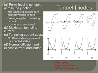
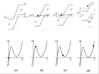
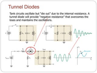
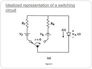
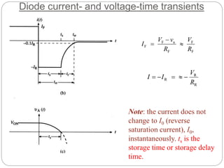
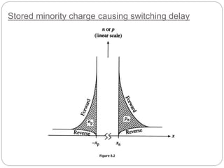
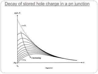
The document discusses tunnel diodes and their switching properties. Tunnel diodes can switch between conducting and non-conducting states at very high speeds due to their narrow depletion widths allowing quantum tunneling. They have short storage times in the nanosecond range. When used as switches, the current in a tunnel diode does not change instantaneously between on and off states, but decays exponentially with a storage delay time ts dictated by the removal of stored minority carriers. Reducing carrier lifetimes and using narrow-base diodes can decrease this switching transient time.


![erf(x) is known as error function and an approximate
solution for storage time can be obtained as
]1ln[
F
p0
F
F
p0
s
R
s
R
I
I
t
II
It
erf
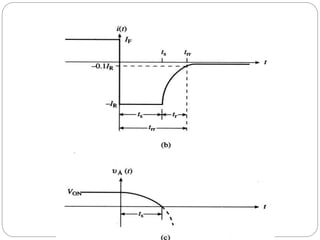
The recovery time t>ts is the time required for the junction
its steady state reverse condition. The reminder of the ex
is being removed and the space charge width is increasin
Bias value .](https://image.slidesharecdn.com/tunneldiode-180523161053/85/Tunnel-diode-26-320.jpg)


![Tunnel_Diode[1].pdffdkjvnfvnfvkgvnjgrjvrgjbbjg](https://cdn.slidesharecdn.com/ss_thumbnails/tunneldiode1-241023150339-31eb82ff-thumbnail.jpg?width=640&height=640&fit=bounds)