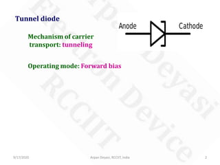
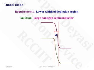
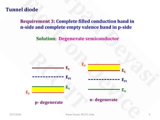
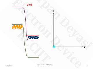
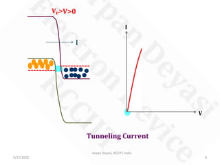
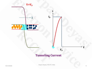
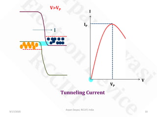
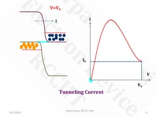
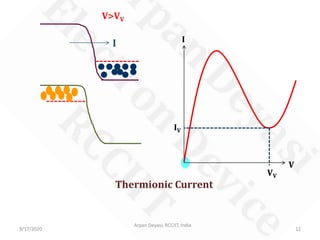
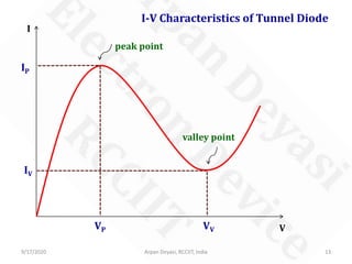
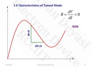
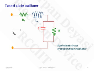
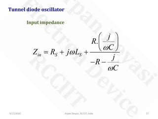
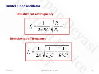
Course: Electronic Devices
paper code: EC301
Course Coordinator: Arpan Deyasi
Department of Electronics and Communication Engineering
RCC Institute of Information Technology
Kolkata, India
9/17/2020 1Arpan Deyasi, RCCIIT, India
Topic: Tunnel Diode
9/17/2020 Arpan Deyasi, RCCIIT, India 2
Tunnel diode
Mechanism of carrier
transport: tunneling
Operating mode: Forward bias
9/17/2020 Arpan Deyasi, RCCIIT, India 3
Criteria for tunneling process
Lower width of depletion region
Lower effective mass
Complete filled conduction band in n-side and
completely empty valence band in p-side
How could these conditions be satisfied?
9/17/2020 Arpan Deyasi, RCCIIT, India 4
Solution: Large bandgap semiconductor
Tunnel diode
Requirement 1: Lower width of depletion region
d
9/17/2020 Arpan Deyasi, RCCIIT, India 5
Solution: Semiconductor with lower effective mass
Tunnel diode
Requirement 2: Lower effective mass
9/17/2020 Arpan Deyasi, RCCIIT, India 6
Solution: Degenerate semiconductor
Tunnel diode
Requirement 3: Complete filled conduction band in
n-side and complete empty valence band in p-side
EC
EV
EFI
EF
n- degenerate
EC
EV
EFI
p- degenerate
EF
9/17/2020
Arpan Deyasi, RCCIIT, India
7
V=0
V
I
9/17/2020
Arpan Deyasi, RCCIIT, India
8
V>0
V
I
I
VP>
Tunneling Current
9/17/2020
Arpan Deyasi, RCCIIT, India
9
V
I
I
V=VP
Tunneling Current
VP
IP
9/17/2020
Arpan Deyasi, RCCIIT, India
10
V
I
I
V>VP
Tunneling Current
IP
VP
9/17/2020
Arpan Deyasi, RCCIIT, India
11
V
II
V=VV
Tunneling Current
VV
IV
9/17/2020
Arpan Deyasi, RCCIIT, India
12
V
II
V>VV
Thermionic Current
VV
IV
9/17/2020 Arpan Deyasi, RCCIIT, India 13
I-V Characteristics of Tunnel Diode
VP VV
IP
IV
peak point
valley point
V
I
9/17/2020 Arpan Deyasi, RCCIIT, India 14
I-V Characteristics of Tunnel Diode
0
dV
R
dI
= <
dV>0
dI<0
V
I
NDR
9/17/2020 Arpan Deyasi, RCCIIT, India 15
Criteria for Tunnel diode operation
Degenerate semiconductor so that Fermi level
should be within the band
Material should have lower effective mass
Large bandgap semiconductor to get thin depletion layer
At operating temperature, all states above Fermi level
should be empty and below Fermi level should be occupied
There must be filled energy states on the side from which
electron will tunnel and allowed empty energy states on
the other side where electron will stay in the same
energy level
9/17/2020 Arpan Deyasi, RCCIIT, India 16
Tunnel diode oscillator
Zin
C
-R
RS LS
Equivalent circuit
of tunnel diode oscillator
9/17/2020 Arpan Deyasi, RCCIIT, India 17
Tunnel diode oscillator
Input impedance
.
in S S
j
R
C
Z R j L
j
R
C
ω
ω
ω
 
 
 = + +
− −
9/17/2020 Arpan Deyasi, RCCIIT, India 18
Tunnel diode oscillator
Resistive cut-off frequency
1
1
2
r
S
R
f
RC Rπ
= −
Reactive cut-off frequency
2 2
1 1 1
2
x
S
f
L C R Cπ
= −

Tunnel diode

  • 1.
    Course: Electronic Devices papercode: EC301 Course Coordinator: Arpan Deyasi Department of Electronics and Communication Engineering RCC Institute of Information Technology Kolkata, India 9/17/2020 1Arpan Deyasi, RCCIIT, India Topic: Tunnel Diode
  • 2.
    9/17/2020 Arpan Deyasi,RCCIIT, India 2 Tunnel diode Mechanism of carrier transport: tunneling Operating mode: Forward bias
  • 3.
    9/17/2020 Arpan Deyasi,RCCIIT, India 3 Criteria for tunneling process Lower width of depletion region Lower effective mass Complete filled conduction band in n-side and completely empty valence band in p-side How could these conditions be satisfied?
  • 4.
    9/17/2020 Arpan Deyasi,RCCIIT, India 4 Solution: Large bandgap semiconductor Tunnel diode Requirement 1: Lower width of depletion region d
  • 5.
    9/17/2020 Arpan Deyasi,RCCIIT, India 5 Solution: Semiconductor with lower effective mass Tunnel diode Requirement 2: Lower effective mass
  • 6.
    9/17/2020 Arpan Deyasi,RCCIIT, India 6 Solution: Degenerate semiconductor Tunnel diode Requirement 3: Complete filled conduction band in n-side and complete empty valence band in p-side EC EV EFI EF n- degenerate EC EV EFI p- degenerate EF
  • 7.
  • 8.
    9/17/2020 Arpan Deyasi, RCCIIT,India 8 V>0 V I I VP> Tunneling Current
  • 9.
    9/17/2020 Arpan Deyasi, RCCIIT,India 9 V I I V=VP Tunneling Current VP IP
  • 10.
    9/17/2020 Arpan Deyasi, RCCIIT,India 10 V I I V>VP Tunneling Current IP VP
  • 11.
    9/17/2020 Arpan Deyasi, RCCIIT,India 11 V II V=VV Tunneling Current VV IV
  • 12.
    9/17/2020 Arpan Deyasi, RCCIIT,India 12 V II V>VV Thermionic Current VV IV
  • 13.
    9/17/2020 Arpan Deyasi,RCCIIT, India 13 I-V Characteristics of Tunnel Diode VP VV IP IV peak point valley point V I
  • 14.
    9/17/2020 Arpan Deyasi,RCCIIT, India 14 I-V Characteristics of Tunnel Diode 0 dV R dI = < dV>0 dI<0 V I NDR
  • 15.
    9/17/2020 Arpan Deyasi,RCCIIT, India 15 Criteria for Tunnel diode operation Degenerate semiconductor so that Fermi level should be within the band Material should have lower effective mass Large bandgap semiconductor to get thin depletion layer At operating temperature, all states above Fermi level should be empty and below Fermi level should be occupied There must be filled energy states on the side from which electron will tunnel and allowed empty energy states on the other side where electron will stay in the same energy level
  • 16.
    9/17/2020 Arpan Deyasi,RCCIIT, India 16 Tunnel diode oscillator Zin C -R RS LS Equivalent circuit of tunnel diode oscillator
  • 17.
    9/17/2020 Arpan Deyasi,RCCIIT, India 17 Tunnel diode oscillator Input impedance . in S S j R C Z R j L j R C ω ω ω      = + + − −
  • 18.
    9/17/2020 Arpan Deyasi,RCCIIT, India 18 Tunnel diode oscillator Resistive cut-off frequency 1 1 2 r S R f RC Rπ = − Reactive cut-off frequency 2 2 1 1 1 2 x S f L C R Cπ = −