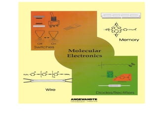
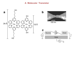
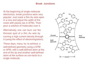
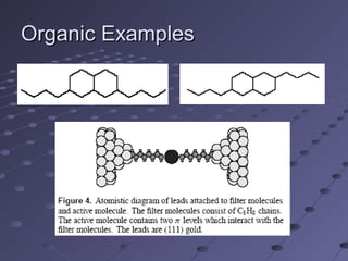
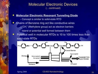
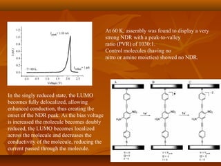
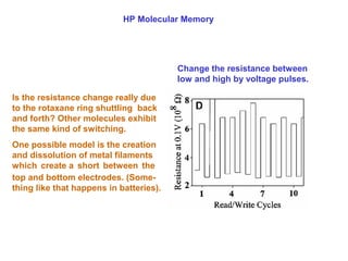
SlideShare a Scribd company logo
Molecular Electronics
Conventional Electronics: Transistor
development
• In 1915 AT&T opened their transcontinental
telephone system; required signal amplification.
• 1945: AT&T and Bell Labs set up the Solid State
Physics group.
• First transistor invented in 1947 at Bell Labs.
• Junction transistors used to develop first integrated
circuit in 1958; Jack Kilby at Texas Instruments (2000
Nobel Prize in Physics).
• FET’s in 1961.
• 1965 Moore’s Law.
Moore’s LawMoore’s Law
Spring 2004 CS-603 Nanotechnology 4
What is Electronic Nanotechnology ?
 Electronic Nanotechnology  Nanoelectronics
 Nanoelectronics: Development of electronic devices
having smallest feature size between 1 to 10 nm
 Possible electronic devices in computers that can be
scaled down to nano levels
- CMOS
- Memory
- Switches
Spring 2004 CS-603 Nanotechnology 5
Approaches To Nanoelectronic Devices
 Two approaches:
- Develop “nano” descendants of present solid-state
microelectronics
- Fabricate nano devices from molecules  Molecular
electronics approach
Path I
Scaling down current S-State devices
Path II
Molecular Electronics
Spring 2004 CS-603 Nanotechnology 6
Promising Nanoelectronic Devices in Future
Computers
 Path I: Nanoelectronic Solid-State Devices
- Nano CMOS
- Resonant Tunneling Diode (RTD)
- Single Electron Transistor (SET)
 Path II: Molecular Electronic Devices
- Molecular Electronic RTD
- Spintronics
Quantum-Effect Devices
Boundaries of conventional techniquesBoundaries of conventional techniques
 Miniaturization achieved by “top down” approach usingMiniaturization achieved by “top down” approach using
improvements in lithography technique.improvements in lithography technique.
 Even with the development of ever-improving lithographicEven with the development of ever-improving lithographic
tools, silicon is approaching fundamental physical limitations oftools, silicon is approaching fundamental physical limitations of
operation. As gate widths decrease below 100 nm, bulkoperation. As gate widths decrease below 100 nm, bulk
properties yield to quantum phenomena and leakage currentsproperties yield to quantum phenomena and leakage currents
from electron tunneling prevent proper device operation.from electron tunneling prevent proper device operation.
 Chemistry operates at the nanometer scale by controlling theChemistry operates at the nanometer scale by controlling the
placement of individual atoms and functional groups onplacement of individual atoms and functional groups on
molecules through synthetic chemistry, allowing macroscopicmolecules through synthetic chemistry, allowing macroscopic
properties from rigidity to optical and electronic behavior to beproperties from rigidity to optical and electronic behavior to be
engineered.engineered.
 ““Bottom up” approach is promising instead of carvingBottom up” approach is promising instead of carving
lithographically bigger blocks into smaller and smaller chunks.lithographically bigger blocks into smaller and smaller chunks.
Molecular ElectronicsMolecular Electronics
 First coined by Mark Ratner, in 1974.First coined by Mark Ratner, in 1974.
 Molecular electronics involves the replacement of aMolecular electronics involves the replacement of a
wire, transistor or other basic solid-state (usuallywire, transistor or other basic solid-state (usually
silicon) electronic element with one or a fewsilicon) electronic element with one or a few
molecules.molecules.
 Molecular electronic device must exchangeMolecular electronic device must exchange
information, or transfer states or must be able toinformation, or transfer states or must be able to
interface with components at the macroscopic level.interface with components at the macroscopic level.
 Simple molecular electronic devices usually consist ofSimple molecular electronic devices usually consist of
organic molecules sandwiched between conductingorganic molecules sandwiched between conducting
electrodes.electrodes.
Inorganic Vs. Organic
Material Properties
Limitations At Early Stage
 Organic materials have often proved to be
unstable.
 Making reliable electrical contacts to organic
thin films is difficult.
 When exposed to air, water, or ultraviolet light,
their electronic properties can degrade rapidly.
 The low carrier mobilities characteristic of
organic materials obviates their use in high-
frequency (greater than 10 MHz) applications.
These shortcomings are compounded by the difficulty of
both purifying and doping the materials.
11
Molecular ElectronicsMolecular Electronics
Aviram-Ratner Diode: an acceptor-bridge-donor moleculeAviram-Ratner Diode: an acceptor-bridge-donor molecule
Chem.Phys.Lett. (1974) 29, 277.Chem.Phys.Lett. (1974) 29, 277.
1. Electrode charge-injection to donor
2. Donor-Acceptor ET
3. Acceptor-electrode charge-injection
A molecular rectifier
Molecular Rectifiers
Molecular RectifiersMolecular Rectifiers
 Metzger and co-workers haveMetzger and co-workers have
studied Langmuir Blodgettstudied Langmuir Blodgett
(LB) films of(LB) films of
(nhexadecyl)quinolinium(nhexadecyl)quinolinium
tricyanoquinodimethanidetricyanoquinodimethanide
between metal electrodes andbetween metal electrodes and
observed strong rectificationobserved strong rectification
behavior.behavior.
The donor is theThe donor is the quinoliniumquinolinium
moiety, connected to themoiety, connected to the
acceptor,acceptor,
tricyanoquinodimethanidetricyanoquinodimethanide
by a bridge.by a bridge.
D-π-A Rectifier
Metzger, R. M. Chem. Rev. 2003, 103, 3803-3834.
I/V curves from two different LB-film configurations. a) 1 LB monolayer b) 4 LB
monolayers.
Metzger, R. M. Chem. Rev. 2003, 103, 3803-3834.
Inorganic Vs. Organic
LEDs
Molecular Orbitals
Organic LED Energy Diagram
Organic Thin Film Transistors
(OTFTs)
Organic material Organic material
An Example of an I-V of OTFTs
Lg = 20 µm
W = 220 µm
400 nm SiO2
50 nm organic
(a) Structures of the long and short linked cobalt coordinated terpyridine thiols used
as gate molecules. (b) A topographic AFM image of the gold electrodes with a gap.
(c) A schematic representation of the assembled single atom transistor.
A Molecular Transistor
A schematic representation of Reed and Tour’s molecular junction containing
a benzene-1,4-dithiolate SAM that bridges two proximal gold electrodes.
Break Junctions
At the beginning of single molecule
electronics, break junctions were very
popular: Just crack a thin Au wire open
in a vice and adjust the width of the
crack with piezos (as in STM). Then
pour a solution of molecules over it.
Alternatively, one can burn out the
thinnest spot of a thin Au wire by
running a high current density through
it (using the effect of electromigration).
These days, many try to achieve a
well-defined geometry using a STM
or AFM, with a well-defined atom at the
end of the tip and another well-defined
atom at the surface as con-tacts to a
single molecule.
LangmuirLangmuir--Blodgett Monolayer PhotodiodeBlodgett Monolayer Photodiode
 ElectrochemicalElectrochemical
photodiode: D-S-Aphotodiode: D-S-A
 Under positive bias, eUnder positive bias, e--
moves from to D to Smoves from to D to S
(G.S).(G.S).
 PhotochemicalPhotochemical
excitation promotes eexcitation promotes e--
to first E.S. of S, to Ato first E.S. of S, to A
and finally to Au.and finally to Au.
 No current when light isNo current when light is
off.off.
Sakomura, M.; Lin, S.; Moore, T. A.; Moore, A. L.; Gust, D.; Fujihira, M.
J. Phys. Chem. A 2002, 106, 2218.
Molecular WiresMolecular Wires
A molecule that connects two (or more)A molecule that connects two (or more)
continuous electron reservoirs, or metalliccontinuous electron reservoirs, or metallic
leadsleads
Organic compoundsOrganic compounds

Usually highly conjugatedUsually highly conjugated
Organometallic compoundsOrganometallic compounds
Organic ExamplesOrganic Examples
Synthesis of “Wires”Synthesis of “Wires”
PolymersPolymers

LinearLinear
PAH’sPAH’s

Conjugation (delocalization) importantConjugation (delocalization) important
Organometallic compoundsOrganometallic compounds
Electrical conduction is desiredElectrical conduction is desired
Insulating the WireInsulating the Wire
More efficientMore efficient
Use of cyclodextrin (a carbohydrate)Use of cyclodextrin (a carbohydrate)
Cyclodextrin used to insulate the molecular wire.
Used to produce green and blue LEDs.
Helps prevent “red shift” from molecular interactions.
CyclodextrinCyclodextrin
Tour WiresTour Wires
James M.Tour’s group over 15 years have been synthesizing moleculesJames M.Tour’s group over 15 years have been synthesizing molecules
with aromatic, alkene, and alkyne bridges, terminating in thiols at one orwith aromatic, alkene, and alkyne bridges, terminating in thiols at one or
both ends. These are known as Tour Wires.both ends. These are known as Tour Wires.
A wire is defined as a two-terminal entity that possesses a reasonably linearA wire is defined as a two-terminal entity that possesses a reasonably linear
I(V) curve prior to the breakdown limit.I(V) curve prior to the breakdown limit.
Precise molecular wires bearing protected alligator clips (SAc) at one and two ends.
Tour Wire: Molecular DevicesTour Wire: Molecular Devices
Molecular devices could be systems having two or more termini with currentMolecular devices could be systems having two or more termini with current--
voltage responses that would be expected to be nonlinear due to intermediatevoltage responses that would be expected to be nonlinear due to intermediate
barriers or heterofunctionalities in the molecular framework.barriers or heterofunctionalities in the molecular framework.
 Two terminal wire with tunnel barrier; wire with a quantum well: RTD; threeTwo terminal wire with tunnel barrier; wire with a quantum well: RTD; three
terminal system: switch; four terminal system: logic gateterminal system: switch; four terminal system: logic gate
Tour, J. M.; Kozaki, M.; Seminario, J. M. J. Am. Chem. Soc. 1998, 120, 8486-8493.
P(m,n) refers to the molecular electrostatic potential impedance of a system with m
1,4-phenylene moieties and n ethynylene moieties.
Spring 2004 CS-603 Nanotechnology 32
Resonant Tunneling Diode (RTD)
 Made by placing insulating barriers on a
semiconductor => creates island or
potential well between them
 Only finite number of discrete energy
levels are permitted in the island
 Electrons can pass through the island by
quantum tunneling
- If incoming electron energy matches (or
resonates) with an energy state inside the
island, then current flows through: “ON”
state
- If energy states inside and outside do not
match: “OFF” state
 Multiple logic states are possible
- As voltage bias is increased and
resonant states are established, switches
“ON. Then switches “OFF” and then
switches “ON” as soon as next level
energy states match
Spring 2004 CS-603 Nanotechnology 33
Molecular Electronic Devices
(…continued)
 Molecular Electronic Resonant Tunneling Diode
- Concept is similar to solid-state RTD
 Chains of Benzene ring act like conductive wires
- “CH2” (Methylene group) act as electron barriers
- Island or potential well formed between them
 Potential well in molecular RTDs is 10 to 100 times less than
solid-state RTDs
Resonant Tunnelling DiodeResonant Tunnelling Diode
 RTD allows voltage bias toRTD allows voltage bias to
switch “on” and “off” theswitch “on” and “off” the
current.current.
 Current passes equally wellCurrent passes equally well
in both directions.in both directions.
 Aliphatic groups with highAliphatic groups with high
P.E. establish aromatic ringP.E. establish aromatic ring
between them as narrowbetween them as narrow
“island” of lower P.E.“island” of lower P.E.
through which electronsthrough which electrons
must pass to traverse themust pass to traverse the
entire length of the wire.entire length of the wire.
Resonant Tunnelling Diode; OperationResonant Tunnelling Diode; Operation
 Smaller the region in which theSmaller the region in which the
electrons are confined, farther apartelectrons are confined, farther apart
are the allowed quantized energyare the allowed quantized energy
levels, eg. “island” and regions tolevels, eg. “island” and regions to
left and right of barrier.left and right of barrier.
 Electrons injected under bias intoElectrons injected under bias into
LUMO on LHS.LUMO on LHS.
 If the K.E. is’nt enough, noIf the K.E. is’nt enough, no
tunneling occurs; switched “off”.tunneling occurs; switched “off”.
 If bias is high enough, incomingIf bias is high enough, incoming
electron’s energy resonate withelectron’s energy resonate with
energy levels inside well, tunnelingenergy levels inside well, tunneling
ocuurs, etc.; switched “on”.ocuurs, etc.; switched “on”.
“Peak” to “valley” ratio ~1.3:1
 A negative differential resistance (NDR) is characterized by a
discontinuity in the monotonic increase of current as the
voltage is increased.
 Several of these devices can be combined to give I/V curves
with multiple peaks–this behavior has been proposed to lead
to multi-state memory and logic devices.
 Reed and Tour et al. reported the clearest example of
molecule-based NDR to date.
Negative Differential Resistance
At 60 K, assembly was found to display a very
strong NDR with a peak-to-valley
ratio (PVR) of 1030:1.
Control molecules (having no
nitro or amine moieties) showed no NDR.
In the singly reduced state, the LUMO
becomes fully delocalized, allowing
enhanced conduction, thus creating the
onset of the NDR peak. As the bias voltage
is increased the molecule becomes doubly
reduced, the LUMO becomes localized
across the molecule and decreases the
conductivity of the molecule, reducing the
current passed through the molecule.
Rotaxane: Molecular SwitchRotaxane: Molecular Switch
 Docking stations:Docking stations:
Benzidine andBenzidine and
Benzophenol.Benzophenol.
 Bulky stopper groups.Bulky stopper groups.
 Bead: tetracationicBead: tetracationic
cyclophane.cyclophane.
 Protonation/Oxidation:Protonation/Oxidation:
bead shifts tobead shifts to
benzophenolbenzophenol
 Molecular shuttleMolecular shuttle
switched electrostaticallyswitched electrostatically
Carroll, R. L.; Gorman, C. B. Angew. Chem. Int. Ed. 2002, 41, 4378-4440.
Rotaxane: Logic DeviceRotaxane: Logic Device
 ““Ring” and “Thread”Ring” and “Thread”
fluoresce separately.fluoresce separately.
 Upon threading (CTUpon threading (CT
complex), fluorescencecomplex), fluorescence
extinguished.extinguished.
 Addition of protons or baseAddition of protons or base
recovers the fluorescence.recovers the fluorescence.
 Neutralization removesNeutralization removes
fluorescence again.fluorescence again.
 If the fluorescence is takenIf the fluorescence is taken
as an indicator of truth, andas an indicator of truth, and
B and HB and H++
are taken as inputs,are taken as inputs,
then the system has thethen the system has the
same behavior as an XORsame behavior as an XOR
gate.gate.
Carroll, R. L.; Gorman, C. B. Angew. Chem. Int. Ed. 2002, 41, 4378-4440.
Rotaxane: Logic DeviceRotaxane: Logic Device
 Tetracationic cyclophaneTetracationic cyclophane
with two bipyridiniumwith two bipyridinium
units interlocked with aunits interlocked with a
crown ether containing acrown ether containing a
TTF and a NP unit onTTF and a NP unit on
opposite sides.opposite sides.
 TTF inside : ATTF inside : A00
 On oxidation, TTFOn oxidation, TTF
outside: Boutside: B++
 At 0 V , goes to BAt 0 V , goes to B00
 Bistability is the basis ofBistability is the basis of
the device.the device.
Stoddart et al. Science 2000, 289, 1172-1175.
Spring 2004 CS-603 Nanotechnology 41
Molecular Electronic Devices for Future Computers
 Molecular Electronics – Uses covalently bonded molecules to
act as wires and switching devices
- Molecules are natural nanometer-scale structures
E.g., A molecular switching device is only 1.5 nm wide!
 Molecular electronics will bring the ultimate revolution in
computing power
- 1 trillion switching devices on a single CPU chip!
- Terabyte level memory capacities!
 Primary advantage – can be synthesized in large numbers; in
the order of Avagadro’s number (1023
)
 Present day challenge is to develop methods to incorporate
these devices in circuits
Spring 2004 CS-603 Nanotechnology 42
Molecular Electronic Devices
(…continued)
 Spintronics
- Spintronics  Spin electronics  Magneto-electronics
- Discovered in 1988 by German and French physicists; IBM
commercialized the concept in 1997
- Exploits the “spin” of electrons, rather than “charge” in information
circuits
- Information is stored into spins as a particular spin orientation (up
or down)
- Spins, being attached to mobile electrons, carry the information
along a wire
 Spin orientation of electrons survive for a relatively longer time,
which makes Spintronic devices attractive for memory storage
devices in computers
40 nm line width, 40 Gbit/inch2
HP Molecular Memory
Output:
Stored
Data
Input:
Address
Molecular Memory
MRAM
(Magnetic Random Access Memory)
Crossbar Memory
Architecture
DRAM
1
0
HP Molecular Memory
The blue ring can shuttle back
and forth along the axis of the
rotaxane molecule, between
the green and red groups.
Rotaxane molecules switch
between high and low resis-
tance by receiving a voltage
pulse.
Collier et al., Science 289, 1172 (2000).
(Many Molecules)
HP Molecular Memory
Change the resistance between
low and high by voltage pulses.
Is the resistance change really due
to the rotaxane ring shuttling back
and forth? Other molecules exhibit
the same kind of switching.
One possible model is the creation
and dissolution of metal filaments
which create a short between the
top and bottom electrodes. (Some-
thing like that happens in batteries).
Quantum
Dot
Molecular Switch
Self-Organizing Memory + Data Processor
Heath et al., Science
280, 1716 (1998)
People have been thinking about
how to combine memory with logic
(= a microprocessor) in a molecular
device.
Self-assembly is the preferred
method. It generates errors, though.
They need to be absorbed by a
fault-tolerant architecture (e.g. in the
HP Teramac)
“Conductivity”
of DNA
Berlin et al., Chem. Phys. 275, 61 (2002)
Tunneling at short distances (independent of temperature)
Hopping at large distances (thermally activated)
Molecular ConductivityMolecular Conductivity
 Electron Transfer:Electron Transfer:
 Coherent nonresonant tunneling :Coherent nonresonant tunneling :
Electronic states of the molecule are far from the energy of theElectronic states of the molecule are far from the energy of the
tunneling electrons; rate of electron transport exponentiallytunneling electrons; rate of electron transport exponentially
dependent on the length of the molecule.dependent on the length of the molecule.
 Coherent resonant tunnelingCoherent resonant tunneling
Energy of tunneling electrons resonant with the energy of theEnergy of tunneling electrons resonant with the energy of the
molecular orbitals’ rate of electron transport is essentiallymolecular orbitals’ rate of electron transport is essentially
independent of length .independent of length .
Spring 2004 CS-603 Nanotechnology 50
Snapshot of Active Research in Nano Devices
Nano
CMOS
RTDs SETs Molecular
Devices
MRAM Hard Drive

    
  
 
 

 
  
ConclusionConclusion
 Molecular electronics will mature into aMolecular electronics will mature into a
powerful technology only if its development ispowerful technology only if its development is
based on sound scientific conclusions thatbased on sound scientific conclusions that
have been tried and tested at every step.have been tried and tested at every step.
 Detailed understanding of theDetailed understanding of the
molecule/electrode interface, as well asmolecule/electrode interface, as well as
developing methods for manufacturing reliabledeveloping methods for manufacturing reliable
devices needed.devices needed.
Possibilities
ENDLESS!!!

More Related Content

What's hot

Metal nanocluster
Metal nanoclusterMetal nanocluster
Metal nanocluster
Sudama04
 
NUCLEAR QUADRUPOLE RESONANCE SPECTROSCOPY
NUCLEAR QUADRUPOLE RESONANCE SPECTROSCOPY NUCLEAR QUADRUPOLE RESONANCE SPECTROSCOPY
NUCLEAR QUADRUPOLE RESONANCE SPECTROSCOPY
Saiva Bhanu Kshatriya College, Aruppukottai.
 
Nanoelectronics
NanoelectronicsNanoelectronics
Nanoelectronics
Aswin Sreeraj
 
Giant magnetoresistance ppt
Giant magnetoresistance pptGiant magnetoresistance ppt
Giant magnetoresistance ppt
tedoado
 
Electron beam lithography
Electron beam lithographyElectron beam lithography
Electron beam lithography
paneliya sagar
 
Thermoelectric materials & Applications
Thermoelectric materials & ApplicationsThermoelectric materials & Applications
Thermoelectric materials & Applications
ut09
 
Single Molecular Magnets: A very Basic Approach to Understand
Single Molecular Magnets: A very Basic Approach to UnderstandSingle Molecular Magnets: A very Basic Approach to Understand
Single Molecular Magnets: A very Basic Approach to Understand
Subhamoy Saha
 
Nanowires presentation
Nanowires presentationNanowires presentation
Nanowires presentation
Tam Van Tran
 
Moletronics 140201085944-phpapp02
Moletronics 140201085944-phpapp02Moletronics 140201085944-phpapp02
Moletronics 140201085944-phpapp02
Surendra Bommavarapu
 
quantum dots and forms of nanomaterials.ppt
quantum dots and forms of nanomaterials.pptquantum dots and forms of nanomaterials.ppt
quantum dots and forms of nanomaterials.ppt
Manju923187
 
ppt
pptppt
computationalchemistry_12-6.ppt
computationalchemistry_12-6.pptcomputationalchemistry_12-6.ppt
computationalchemistry_12-6.ppt
sami97008
 
Fabrication and characterization of nanowire devices
Fabrication and characterization of nanowire devicesFabrication and characterization of nanowire devices
Fabrication and characterization of nanowire devices
Eternal University Baru Sahib, HP, India
 
Moletronics or molecular electronics - technical seminar
Moletronics or molecular electronics - technical seminarMoletronics or molecular electronics - technical seminar
Moletronics or molecular electronics - technical seminar
SUKHWINDER SINGH
 
Molecular Electronics
Molecular ElectronicsMolecular Electronics
Molecular Electronics
Valentina Ferro
 
quantum dots
quantum dotsquantum dots
quantum dots
Hoang Tien
 
Hemocyanin and Hemerythrin
Hemocyanin and HemerythrinHemocyanin and Hemerythrin
Hemocyanin and Hemerythrin
SantarupaThakurta
 
nano science and nano technology
nano science and nano technologynano science and nano technology
nano science and nano technology
Anmol Bagga
 
Band structure and surface properties of 1-4 layers of MoS2
Band structure and surface properties of 1-4 layers of MoS2Band structure and surface properties of 1-4 layers of MoS2
Band structure and surface properties of 1-4 layers of MoS2
Po-Chun Yeh
 
Four probe Method.pptx
Four probe Method.pptxFour probe Method.pptx
Four probe Method.pptx
JatinMahato1
 

What's hot (20)

Metal nanocluster
Metal nanoclusterMetal nanocluster
Metal nanocluster
 
NUCLEAR QUADRUPOLE RESONANCE SPECTROSCOPY
NUCLEAR QUADRUPOLE RESONANCE SPECTROSCOPY NUCLEAR QUADRUPOLE RESONANCE SPECTROSCOPY
NUCLEAR QUADRUPOLE RESONANCE SPECTROSCOPY
 
Nanoelectronics
NanoelectronicsNanoelectronics
Nanoelectronics
 
Giant magnetoresistance ppt
Giant magnetoresistance pptGiant magnetoresistance ppt
Giant magnetoresistance ppt
 
Electron beam lithography
Electron beam lithographyElectron beam lithography
Electron beam lithography
 
Thermoelectric materials & Applications
Thermoelectric materials & ApplicationsThermoelectric materials & Applications
Thermoelectric materials & Applications
 
Single Molecular Magnets: A very Basic Approach to Understand
Single Molecular Magnets: A very Basic Approach to UnderstandSingle Molecular Magnets: A very Basic Approach to Understand
Single Molecular Magnets: A very Basic Approach to Understand
 
Nanowires presentation
Nanowires presentationNanowires presentation
Nanowires presentation
 
Moletronics 140201085944-phpapp02
Moletronics 140201085944-phpapp02Moletronics 140201085944-phpapp02
Moletronics 140201085944-phpapp02
 
quantum dots and forms of nanomaterials.ppt
quantum dots and forms of nanomaterials.pptquantum dots and forms of nanomaterials.ppt
quantum dots and forms of nanomaterials.ppt
 
ppt
pptppt
ppt
 
computationalchemistry_12-6.ppt
computationalchemistry_12-6.pptcomputationalchemistry_12-6.ppt
computationalchemistry_12-6.ppt
 
Fabrication and characterization of nanowire devices
Fabrication and characterization of nanowire devicesFabrication and characterization of nanowire devices
Fabrication and characterization of nanowire devices
 
Moletronics or molecular electronics - technical seminar
Moletronics or molecular electronics - technical seminarMoletronics or molecular electronics - technical seminar
Moletronics or molecular electronics - technical seminar
 
Molecular Electronics
Molecular ElectronicsMolecular Electronics
Molecular Electronics
 
quantum dots
quantum dotsquantum dots
quantum dots
 
Hemocyanin and Hemerythrin
Hemocyanin and HemerythrinHemocyanin and Hemerythrin
Hemocyanin and Hemerythrin
 
nano science and nano technology
nano science and nano technologynano science and nano technology
nano science and nano technology
 
Band structure and surface properties of 1-4 layers of MoS2
Band structure and surface properties of 1-4 layers of MoS2Band structure and surface properties of 1-4 layers of MoS2
Band structure and surface properties of 1-4 layers of MoS2
 
Four probe Method.pptx
Four probe Method.pptxFour probe Method.pptx
Four probe Method.pptx
 

Similar to Molecular electronics

NANOELECTRONICS-ppt.ppt
NANOELECTRONICS-ppt.pptNANOELECTRONICS-ppt.ppt
NANOELECTRONICS-ppt.ppt
DevanandhKoroth
 
cathode ray oscilloscope
cathode ray oscilloscopecathode ray oscilloscope
cathode ray oscilloscope
hajahrokiah
 
Memrstror
MemrstrorMemrstror
Memrstror
satyamrebel
 
322253456-NANOELECTRONICS-ppt of engineering
322253456-NANOELECTRONICS-ppt of engineering322253456-NANOELECTRONICS-ppt of engineering
322253456-NANOELECTRONICS-ppt of engineering
t24042567
 
Semiconductor
SemiconductorSemiconductor
Semiconductor
Yong Heui Cho
 
Thermionic emission
Thermionic emissionThermionic emission
Thermionic emission
KAZEMBETVOnline
 
Memristor
MemristorMemristor
L-3-4 Introduction to electroceramics.pptx
L-3-4 Introduction to electroceramics.pptxL-3-4 Introduction to electroceramics.pptx
L-3-4 Introduction to electroceramics.pptx
PUNAMK4
 
Spin valve transistor
Spin valve transistorSpin valve transistor
Spin valve transistor
Eeshan Mishra
 
Electronic devices chapter 1- 3 (m.sc physics)
Electronic devices chapter 1- 3 (m.sc physics)Electronic devices chapter 1- 3 (m.sc physics)
Electronic devices chapter 1- 3 (m.sc physics)
Ali Farooq
 
Jas powerpoint new
Jas powerpoint newJas powerpoint new
Jas powerpoint new
Dith Jose
 
Microelectrodes ch01
Microelectrodes ch01Microelectrodes ch01
Microelectrodes ch01
Mukesh Samta
 
How is electricity_produced
How is electricity_producedHow is electricity_produced
How is electricity_produced
Mar Sanchez Osuna
 
FARAMARZI_Vina_2011
FARAMARZI_Vina_2011FARAMARZI_Vina_2011
FARAMARZI_Vina_2011
Vina Faramarzi
 
VTU Seminar FULL report LATEST
VTU Seminar FULL report LATESTVTU Seminar FULL report LATEST
VTU Seminar FULL report LATEST
athiathi3
 
Lecture 01 Introduction and applications of Electronics & SemiConductors.pdf
Lecture 01 Introduction and applications of Electronics & SemiConductors.pdfLecture 01 Introduction and applications of Electronics & SemiConductors.pdf
Lecture 01 Introduction and applications of Electronics & SemiConductors.pdf
Athar Baig
 
X Ray Production
X Ray ProductionX Ray Production
X Ray Production
Anees Muhammed
 
A Study of electromechanical behavior of Piezo ceramic Smart materials and ap...
A Study of electromechanical behavior of Piezo ceramic Smart materials and ap...A Study of electromechanical behavior of Piezo ceramic Smart materials and ap...
A Study of electromechanical behavior of Piezo ceramic Smart materials and ap...
Dheepan Thangavelu
 
English for Electric and Electronic Engineering
English for Electric and Electronic EngineeringEnglish for Electric and Electronic Engineering
English for Electric and Electronic Engineering
HOng Thuong Hoang
 
Spintronics combination of nanotechnology & superconductivity
Spintronics combination of nanotechnology & superconductivitySpintronics combination of nanotechnology & superconductivity
Spintronics combination of nanotechnology & superconductivity
Alexander Decker
 

Similar to Molecular electronics (20)

NANOELECTRONICS-ppt.ppt
NANOELECTRONICS-ppt.pptNANOELECTRONICS-ppt.ppt
NANOELECTRONICS-ppt.ppt
 
cathode ray oscilloscope
cathode ray oscilloscopecathode ray oscilloscope
cathode ray oscilloscope
 
Memrstror
MemrstrorMemrstror
Memrstror
 
322253456-NANOELECTRONICS-ppt of engineering
322253456-NANOELECTRONICS-ppt of engineering322253456-NANOELECTRONICS-ppt of engineering
322253456-NANOELECTRONICS-ppt of engineering
 
Semiconductor
SemiconductorSemiconductor
Semiconductor
 
Thermionic emission
Thermionic emissionThermionic emission
Thermionic emission
 
Memristor
MemristorMemristor
Memristor
 
L-3-4 Introduction to electroceramics.pptx
L-3-4 Introduction to electroceramics.pptxL-3-4 Introduction to electroceramics.pptx
L-3-4 Introduction to electroceramics.pptx
 
Spin valve transistor
Spin valve transistorSpin valve transistor
Spin valve transistor
 
Electronic devices chapter 1- 3 (m.sc physics)
Electronic devices chapter 1- 3 (m.sc physics)Electronic devices chapter 1- 3 (m.sc physics)
Electronic devices chapter 1- 3 (m.sc physics)
 
Jas powerpoint new
Jas powerpoint newJas powerpoint new
Jas powerpoint new
 
Microelectrodes ch01
Microelectrodes ch01Microelectrodes ch01
Microelectrodes ch01
 
How is electricity_produced
How is electricity_producedHow is electricity_produced
How is electricity_produced
 
FARAMARZI_Vina_2011
FARAMARZI_Vina_2011FARAMARZI_Vina_2011
FARAMARZI_Vina_2011
 
VTU Seminar FULL report LATEST
VTU Seminar FULL report LATESTVTU Seminar FULL report LATEST
VTU Seminar FULL report LATEST
 
Lecture 01 Introduction and applications of Electronics & SemiConductors.pdf
Lecture 01 Introduction and applications of Electronics & SemiConductors.pdfLecture 01 Introduction and applications of Electronics & SemiConductors.pdf
Lecture 01 Introduction and applications of Electronics & SemiConductors.pdf
 
X Ray Production
X Ray ProductionX Ray Production
X Ray Production
 
A Study of electromechanical behavior of Piezo ceramic Smart materials and ap...
A Study of electromechanical behavior of Piezo ceramic Smart materials and ap...A Study of electromechanical behavior of Piezo ceramic Smart materials and ap...
A Study of electromechanical behavior of Piezo ceramic Smart materials and ap...
 
English for Electric and Electronic Engineering
English for Electric and Electronic EngineeringEnglish for Electric and Electronic Engineering
English for Electric and Electronic Engineering
 
Spintronics combination of nanotechnology & superconductivity
Spintronics combination of nanotechnology & superconductivitySpintronics combination of nanotechnology & superconductivity
Spintronics combination of nanotechnology & superconductivity
 

More from utpal sarkar

Rom ram
Rom ramRom ram
Rom ram
utpal sarkar
 
Pressure sensor lecture
Pressure sensor lecturePressure sensor lecture
Pressure sensor lecture
utpal sarkar
 
Optical properties and hall effect
Optical properties and hall effectOptical properties and hall effect
Optical properties and hall effect
utpal sarkar
 
Tunnel diode
Tunnel diodeTunnel diode
Tunnel diode
utpal sarkar
 
Night vission
Night vissionNight vission
Night vission
utpal sarkar
 
Night vision goggles the basics
Night vision goggles the basicsNight vision goggles the basics
Night vision goggles the basics
utpal sarkar
 
Nano electro mechanical systems
Nano electro mechanical systems Nano electro mechanical systems
Nano electro mechanical systems
utpal sarkar
 
Metal Insulator Semiconductor devices
Metal Insulator Semiconductor devicesMetal Insulator Semiconductor devices
Metal Insulator Semiconductor devices
utpal sarkar
 
Metal Oxide Semiconductor Field Effect Transistors
Metal Oxide Semiconductor Field Effect TransistorsMetal Oxide Semiconductor Field Effect Transistors
Metal Oxide Semiconductor Field Effect Transistors
utpal sarkar
 
Micro-electro-mechanical Systems
Micro-electro-mechanical Systems Micro-electro-mechanical Systems
Micro-electro-mechanical Systems
utpal sarkar
 
Introduction to Sensor
Introduction to SensorIntroduction to Sensor
Introduction to Sensor
utpal sarkar
 
Introduction to Sensors
Introduction to Sensors  Introduction to Sensors
Introduction to Sensors
utpal sarkar
 
Pacemakers
PacemakersPacemakers
Pacemakers
utpal sarkar
 
Sensor Biomedical applications
 Sensor Biomedical applications Sensor Biomedical applications
Sensor Biomedical applications
utpal sarkar
 
Sensor Lecture Interfacing
 Sensor Lecture Interfacing Sensor Lecture Interfacing
Sensor Lecture Interfacing
utpal sarkar
 
Nano twzeeres
Nano twzeeresNano twzeeres
Nano twzeeres
utpal sarkar
 
Ink Jet Nozzels
Ink Jet NozzelsInk Jet Nozzels
Ink Jet Nozzels
utpal sarkar
 
Night Vision Technology
Night Vision Technology Night Vision Technology
Night Vision Technology
utpal sarkar
 
Band theory of solids
Band theory of solidsBand theory of solids
Band theory of solids
utpal sarkar
 
Accelerometers
AccelerometersAccelerometers
Accelerometers
utpal sarkar
 

More from utpal sarkar (20)

Rom ram
Rom ramRom ram
Rom ram
 
Pressure sensor lecture
Pressure sensor lecturePressure sensor lecture
Pressure sensor lecture
 
Optical properties and hall effect
Optical properties and hall effectOptical properties and hall effect
Optical properties and hall effect
 
Tunnel diode
Tunnel diodeTunnel diode
Tunnel diode
 
Night vission
Night vissionNight vission
Night vission
 
Night vision goggles the basics
Night vision goggles the basicsNight vision goggles the basics
Night vision goggles the basics
 
Nano electro mechanical systems
Nano electro mechanical systems Nano electro mechanical systems
Nano electro mechanical systems
 
Metal Insulator Semiconductor devices
Metal Insulator Semiconductor devicesMetal Insulator Semiconductor devices
Metal Insulator Semiconductor devices
 
Metal Oxide Semiconductor Field Effect Transistors
Metal Oxide Semiconductor Field Effect TransistorsMetal Oxide Semiconductor Field Effect Transistors
Metal Oxide Semiconductor Field Effect Transistors
 
Micro-electro-mechanical Systems
Micro-electro-mechanical Systems Micro-electro-mechanical Systems
Micro-electro-mechanical Systems
 
Introduction to Sensor
Introduction to SensorIntroduction to Sensor
Introduction to Sensor
 
Introduction to Sensors
Introduction to Sensors  Introduction to Sensors
Introduction to Sensors
 
Pacemakers
PacemakersPacemakers
Pacemakers
 
Sensor Biomedical applications
 Sensor Biomedical applications Sensor Biomedical applications
Sensor Biomedical applications
 
Sensor Lecture Interfacing
 Sensor Lecture Interfacing Sensor Lecture Interfacing
Sensor Lecture Interfacing
 
Nano twzeeres
Nano twzeeresNano twzeeres
Nano twzeeres
 
Ink Jet Nozzels
Ink Jet NozzelsInk Jet Nozzels
Ink Jet Nozzels
 
Night Vision Technology
Night Vision Technology Night Vision Technology
Night Vision Technology
 
Band theory of solids
Band theory of solidsBand theory of solids
Band theory of solids
 
Accelerometers
AccelerometersAccelerometers
Accelerometers
 

Recently uploaded

UiPath Test Automation using UiPath Test Suite series, part 5
UiPath Test Automation using UiPath Test Suite series, part 5UiPath Test Automation using UiPath Test Suite series, part 5
UiPath Test Automation using UiPath Test Suite series, part 5
DianaGray10
 
“Building and Scaling AI Applications with the Nx AI Manager,” a Presentation...
“Building and Scaling AI Applications with the Nx AI Manager,” a Presentation...“Building and Scaling AI Applications with the Nx AI Manager,” a Presentation...
“Building and Scaling AI Applications with the Nx AI Manager,” a Presentation...
Edge AI and Vision Alliance
 
Video Streaming: Then, Now, and in the Future
Video Streaming: Then, Now, and in the FutureVideo Streaming: Then, Now, and in the Future
Video Streaming: Then, Now, and in the Future
Alpen-Adria-Universität
 
National Security Agency - NSA mobile device best practices
National Security Agency - NSA mobile device best practicesNational Security Agency - NSA mobile device best practices
National Security Agency - NSA mobile device best practices
Quotidiano Piemontese
 
Generative AI Deep Dive: Advancing from Proof of Concept to Production
Generative AI Deep Dive: Advancing from Proof of Concept to ProductionGenerative AI Deep Dive: Advancing from Proof of Concept to Production
Generative AI Deep Dive: Advancing from Proof of Concept to Production
Aggregage
 
GraphSummit Singapore | Graphing Success: Revolutionising Organisational Stru...
GraphSummit Singapore | Graphing Success: Revolutionising Organisational Stru...GraphSummit Singapore | Graphing Success: Revolutionising Organisational Stru...
GraphSummit Singapore | Graphing Success: Revolutionising Organisational Stru...
Neo4j
 
Encryption in Microsoft 365 - ExpertsLive Netherlands 2024
Encryption in Microsoft 365 - ExpertsLive Netherlands 2024Encryption in Microsoft 365 - ExpertsLive Netherlands 2024
Encryption in Microsoft 365 - ExpertsLive Netherlands 2024
Albert Hoitingh
 
Securing your Kubernetes cluster_ a step-by-step guide to success !
Securing your Kubernetes cluster_ a step-by-step guide to success !Securing your Kubernetes cluster_ a step-by-step guide to success !
Securing your Kubernetes cluster_ a step-by-step guide to success !
KatiaHIMEUR1
 
Removing Uninteresting Bytes in Software Fuzzing
Removing Uninteresting Bytes in Software FuzzingRemoving Uninteresting Bytes in Software Fuzzing
Removing Uninteresting Bytes in Software Fuzzing
Aftab Hussain
 
GraphSummit Singapore | The Future of Agility: Supercharging Digital Transfor...
GraphSummit Singapore | The Future of Agility: Supercharging Digital Transfor...GraphSummit Singapore | The Future of Agility: Supercharging Digital Transfor...
GraphSummit Singapore | The Future of Agility: Supercharging Digital Transfor...
Neo4j
 
A tale of scale & speed: How the US Navy is enabling software delivery from l...
A tale of scale & speed: How the US Navy is enabling software delivery from l...A tale of scale & speed: How the US Navy is enabling software delivery from l...
A tale of scale & speed: How the US Navy is enabling software delivery from l...
sonjaschweigert1
 
Introducing Milvus Lite: Easy-to-Install, Easy-to-Use vector database for you...
Introducing Milvus Lite: Easy-to-Install, Easy-to-Use vector database for you...Introducing Milvus Lite: Easy-to-Install, Easy-to-Use vector database for you...
Introducing Milvus Lite: Easy-to-Install, Easy-to-Use vector database for you...
Zilliz
 
みなさんこんにちはこれ何文字まで入るの?40文字以下不可とか本当に意味わからないけどこれ限界文字数書いてないからマジでやばい文字数いけるんじゃないの?えこ...
みなさんこんにちはこれ何文字まで入るの?40文字以下不可とか本当に意味わからないけどこれ限界文字数書いてないからマジでやばい文字数いけるんじゃないの?えこ...みなさんこんにちはこれ何文字まで入るの?40文字以下不可とか本当に意味わからないけどこれ限界文字数書いてないからマジでやばい文字数いけるんじゃないの?えこ...
みなさんこんにちはこれ何文字まで入るの?40文字以下不可とか本当に意味わからないけどこれ限界文字数書いてないからマジでやばい文字数いけるんじゃないの?えこ...
名前 です男
 
20240609 QFM020 Irresponsible AI Reading List May 2024
20240609 QFM020 Irresponsible AI Reading List May 202420240609 QFM020 Irresponsible AI Reading List May 2024
20240609 QFM020 Irresponsible AI Reading List May 2024
Matthew Sinclair
 
Observability Concepts EVERY Developer Should Know -- DeveloperWeek Europe.pdf
Observability Concepts EVERY Developer Should Know -- DeveloperWeek Europe.pdfObservability Concepts EVERY Developer Should Know -- DeveloperWeek Europe.pdf
Observability Concepts EVERY Developer Should Know -- DeveloperWeek Europe.pdf
Paige Cruz
 
“I’m still / I’m still / Chaining from the Block”
“I’m still / I’m still / Chaining from the Block”“I’m still / I’m still / Chaining from the Block”
“I’m still / I’m still / Chaining from the Block”
Claudio Di Ciccio
 
Mind map of terminologies used in context of Generative AI
Mind map of terminologies used in context of Generative AIMind map of terminologies used in context of Generative AI
Mind map of terminologies used in context of Generative AI
Kumud Singh
 
Communications Mining Series - Zero to Hero - Session 1
Communications Mining Series - Zero to Hero - Session 1Communications Mining Series - Zero to Hero - Session 1
Communications Mining Series - Zero to Hero - Session 1
DianaGray10
 
RESUME BUILDER APPLICATION Project for students
RESUME BUILDER APPLICATION Project for studentsRESUME BUILDER APPLICATION Project for students
RESUME BUILDER APPLICATION Project for students
KAMESHS29
 
Let's Integrate MuleSoft RPA, COMPOSER, APM with AWS IDP along with Slack
Let's Integrate MuleSoft RPA, COMPOSER, APM with AWS IDP along with SlackLet's Integrate MuleSoft RPA, COMPOSER, APM with AWS IDP along with Slack
Let's Integrate MuleSoft RPA, COMPOSER, APM with AWS IDP along with Slack
shyamraj55
 

Recently uploaded (20)

UiPath Test Automation using UiPath Test Suite series, part 5
UiPath Test Automation using UiPath Test Suite series, part 5UiPath Test Automation using UiPath Test Suite series, part 5
UiPath Test Automation using UiPath Test Suite series, part 5
 
“Building and Scaling AI Applications with the Nx AI Manager,” a Presentation...
“Building and Scaling AI Applications with the Nx AI Manager,” a Presentation...“Building and Scaling AI Applications with the Nx AI Manager,” a Presentation...
“Building and Scaling AI Applications with the Nx AI Manager,” a Presentation...
 
Video Streaming: Then, Now, and in the Future
Video Streaming: Then, Now, and in the FutureVideo Streaming: Then, Now, and in the Future
Video Streaming: Then, Now, and in the Future
 
National Security Agency - NSA mobile device best practices
National Security Agency - NSA mobile device best practicesNational Security Agency - NSA mobile device best practices
National Security Agency - NSA mobile device best practices
 
Generative AI Deep Dive: Advancing from Proof of Concept to Production
Generative AI Deep Dive: Advancing from Proof of Concept to ProductionGenerative AI Deep Dive: Advancing from Proof of Concept to Production
Generative AI Deep Dive: Advancing from Proof of Concept to Production
 
GraphSummit Singapore | Graphing Success: Revolutionising Organisational Stru...
GraphSummit Singapore | Graphing Success: Revolutionising Organisational Stru...GraphSummit Singapore | Graphing Success: Revolutionising Organisational Stru...
GraphSummit Singapore | Graphing Success: Revolutionising Organisational Stru...
 
Encryption in Microsoft 365 - ExpertsLive Netherlands 2024
Encryption in Microsoft 365 - ExpertsLive Netherlands 2024Encryption in Microsoft 365 - ExpertsLive Netherlands 2024
Encryption in Microsoft 365 - ExpertsLive Netherlands 2024
 
Securing your Kubernetes cluster_ a step-by-step guide to success !
Securing your Kubernetes cluster_ a step-by-step guide to success !Securing your Kubernetes cluster_ a step-by-step guide to success !
Securing your Kubernetes cluster_ a step-by-step guide to success !
 
Removing Uninteresting Bytes in Software Fuzzing
Removing Uninteresting Bytes in Software FuzzingRemoving Uninteresting Bytes in Software Fuzzing
Removing Uninteresting Bytes in Software Fuzzing
 
GraphSummit Singapore | The Future of Agility: Supercharging Digital Transfor...
GraphSummit Singapore | The Future of Agility: Supercharging Digital Transfor...GraphSummit Singapore | The Future of Agility: Supercharging Digital Transfor...
GraphSummit Singapore | The Future of Agility: Supercharging Digital Transfor...
 
A tale of scale & speed: How the US Navy is enabling software delivery from l...
A tale of scale & speed: How the US Navy is enabling software delivery from l...A tale of scale & speed: How the US Navy is enabling software delivery from l...
A tale of scale & speed: How the US Navy is enabling software delivery from l...
 
Introducing Milvus Lite: Easy-to-Install, Easy-to-Use vector database for you...
Introducing Milvus Lite: Easy-to-Install, Easy-to-Use vector database for you...Introducing Milvus Lite: Easy-to-Install, Easy-to-Use vector database for you...
Introducing Milvus Lite: Easy-to-Install, Easy-to-Use vector database for you...
 
みなさんこんにちはこれ何文字まで入るの?40文字以下不可とか本当に意味わからないけどこれ限界文字数書いてないからマジでやばい文字数いけるんじゃないの?えこ...
みなさんこんにちはこれ何文字まで入るの?40文字以下不可とか本当に意味わからないけどこれ限界文字数書いてないからマジでやばい文字数いけるんじゃないの?えこ...みなさんこんにちはこれ何文字まで入るの?40文字以下不可とか本当に意味わからないけどこれ限界文字数書いてないからマジでやばい文字数いけるんじゃないの?えこ...
みなさんこんにちはこれ何文字まで入るの?40文字以下不可とか本当に意味わからないけどこれ限界文字数書いてないからマジでやばい文字数いけるんじゃないの?えこ...
 
20240609 QFM020 Irresponsible AI Reading List May 2024
20240609 QFM020 Irresponsible AI Reading List May 202420240609 QFM020 Irresponsible AI Reading List May 2024
20240609 QFM020 Irresponsible AI Reading List May 2024
 
Observability Concepts EVERY Developer Should Know -- DeveloperWeek Europe.pdf
Observability Concepts EVERY Developer Should Know -- DeveloperWeek Europe.pdfObservability Concepts EVERY Developer Should Know -- DeveloperWeek Europe.pdf
Observability Concepts EVERY Developer Should Know -- DeveloperWeek Europe.pdf
 
“I’m still / I’m still / Chaining from the Block”
“I’m still / I’m still / Chaining from the Block”“I’m still / I’m still / Chaining from the Block”
“I’m still / I’m still / Chaining from the Block”
 
Mind map of terminologies used in context of Generative AI
Mind map of terminologies used in context of Generative AIMind map of terminologies used in context of Generative AI
Mind map of terminologies used in context of Generative AI
 
Communications Mining Series - Zero to Hero - Session 1
Communications Mining Series - Zero to Hero - Session 1Communications Mining Series - Zero to Hero - Session 1
Communications Mining Series - Zero to Hero - Session 1
 
RESUME BUILDER APPLICATION Project for students
RESUME BUILDER APPLICATION Project for studentsRESUME BUILDER APPLICATION Project for students
RESUME BUILDER APPLICATION Project for students
 
Let's Integrate MuleSoft RPA, COMPOSER, APM with AWS IDP along with Slack
Let's Integrate MuleSoft RPA, COMPOSER, APM with AWS IDP along with SlackLet's Integrate MuleSoft RPA, COMPOSER, APM with AWS IDP along with Slack
Let's Integrate MuleSoft RPA, COMPOSER, APM with AWS IDP along with Slack
 

Molecular electronics

  • 2. Conventional Electronics: Transistor development • In 1915 AT&T opened their transcontinental telephone system; required signal amplification. • 1945: AT&T and Bell Labs set up the Solid State Physics group. • First transistor invented in 1947 at Bell Labs. • Junction transistors used to develop first integrated circuit in 1958; Jack Kilby at Texas Instruments (2000 Nobel Prize in Physics). • FET’s in 1961. • 1965 Moore’s Law.
  • 4. Spring 2004 CS-603 Nanotechnology 4 What is Electronic Nanotechnology ?  Electronic Nanotechnology  Nanoelectronics  Nanoelectronics: Development of electronic devices having smallest feature size between 1 to 10 nm  Possible electronic devices in computers that can be scaled down to nano levels - CMOS - Memory - Switches
  • 5. Spring 2004 CS-603 Nanotechnology 5 Approaches To Nanoelectronic Devices  Two approaches: - Develop “nano” descendants of present solid-state microelectronics - Fabricate nano devices from molecules  Molecular electronics approach Path I Scaling down current S-State devices Path II Molecular Electronics
  • 6. Spring 2004 CS-603 Nanotechnology 6 Promising Nanoelectronic Devices in Future Computers  Path I: Nanoelectronic Solid-State Devices - Nano CMOS - Resonant Tunneling Diode (RTD) - Single Electron Transistor (SET)  Path II: Molecular Electronic Devices - Molecular Electronic RTD - Spintronics Quantum-Effect Devices
  • 7. Boundaries of conventional techniquesBoundaries of conventional techniques  Miniaturization achieved by “top down” approach usingMiniaturization achieved by “top down” approach using improvements in lithography technique.improvements in lithography technique.  Even with the development of ever-improving lithographicEven with the development of ever-improving lithographic tools, silicon is approaching fundamental physical limitations oftools, silicon is approaching fundamental physical limitations of operation. As gate widths decrease below 100 nm, bulkoperation. As gate widths decrease below 100 nm, bulk properties yield to quantum phenomena and leakage currentsproperties yield to quantum phenomena and leakage currents from electron tunneling prevent proper device operation.from electron tunneling prevent proper device operation.  Chemistry operates at the nanometer scale by controlling theChemistry operates at the nanometer scale by controlling the placement of individual atoms and functional groups onplacement of individual atoms and functional groups on molecules through synthetic chemistry, allowing macroscopicmolecules through synthetic chemistry, allowing macroscopic properties from rigidity to optical and electronic behavior to beproperties from rigidity to optical and electronic behavior to be engineered.engineered.  ““Bottom up” approach is promising instead of carvingBottom up” approach is promising instead of carving lithographically bigger blocks into smaller and smaller chunks.lithographically bigger blocks into smaller and smaller chunks.
  • 8. Molecular ElectronicsMolecular Electronics  First coined by Mark Ratner, in 1974.First coined by Mark Ratner, in 1974.  Molecular electronics involves the replacement of aMolecular electronics involves the replacement of a wire, transistor or other basic solid-state (usuallywire, transistor or other basic solid-state (usually silicon) electronic element with one or a fewsilicon) electronic element with one or a few molecules.molecules.  Molecular electronic device must exchangeMolecular electronic device must exchange information, or transfer states or must be able toinformation, or transfer states or must be able to interface with components at the macroscopic level.interface with components at the macroscopic level.  Simple molecular electronic devices usually consist ofSimple molecular electronic devices usually consist of organic molecules sandwiched between conductingorganic molecules sandwiched between conducting electrodes.electrodes.
  • 10. Limitations At Early Stage  Organic materials have often proved to be unstable.  Making reliable electrical contacts to organic thin films is difficult.  When exposed to air, water, or ultraviolet light, their electronic properties can degrade rapidly.  The low carrier mobilities characteristic of organic materials obviates their use in high- frequency (greater than 10 MHz) applications. These shortcomings are compounded by the difficulty of both purifying and doping the materials.
  • 11. 11 Molecular ElectronicsMolecular Electronics Aviram-Ratner Diode: an acceptor-bridge-donor moleculeAviram-Ratner Diode: an acceptor-bridge-donor molecule Chem.Phys.Lett. (1974) 29, 277.Chem.Phys.Lett. (1974) 29, 277. 1. Electrode charge-injection to donor 2. Donor-Acceptor ET 3. Acceptor-electrode charge-injection A molecular rectifier
  • 13. Molecular RectifiersMolecular Rectifiers  Metzger and co-workers haveMetzger and co-workers have studied Langmuir Blodgettstudied Langmuir Blodgett (LB) films of(LB) films of (nhexadecyl)quinolinium(nhexadecyl)quinolinium tricyanoquinodimethanidetricyanoquinodimethanide between metal electrodes andbetween metal electrodes and observed strong rectificationobserved strong rectification behavior.behavior. The donor is theThe donor is the quinoliniumquinolinium moiety, connected to themoiety, connected to the acceptor,acceptor, tricyanoquinodimethanidetricyanoquinodimethanide by a bridge.by a bridge. D-π-A Rectifier Metzger, R. M. Chem. Rev. 2003, 103, 3803-3834.
  • 14. I/V curves from two different LB-film configurations. a) 1 LB monolayer b) 4 LB monolayers. Metzger, R. M. Chem. Rev. 2003, 103, 3803-3834.
  • 18. Organic Thin Film Transistors (OTFTs) Organic material Organic material
  • 19. An Example of an I-V of OTFTs Lg = 20 µm W = 220 µm 400 nm SiO2 50 nm organic
  • 20.
  • 21. (a) Structures of the long and short linked cobalt coordinated terpyridine thiols used as gate molecules. (b) A topographic AFM image of the gold electrodes with a gap. (c) A schematic representation of the assembled single atom transistor. A Molecular Transistor
  • 22. A schematic representation of Reed and Tour’s molecular junction containing a benzene-1,4-dithiolate SAM that bridges two proximal gold electrodes. Break Junctions At the beginning of single molecule electronics, break junctions were very popular: Just crack a thin Au wire open in a vice and adjust the width of the crack with piezos (as in STM). Then pour a solution of molecules over it. Alternatively, one can burn out the thinnest spot of a thin Au wire by running a high current density through it (using the effect of electromigration). These days, many try to achieve a well-defined geometry using a STM or AFM, with a well-defined atom at the end of the tip and another well-defined atom at the surface as con-tacts to a single molecule.
  • 23. LangmuirLangmuir--Blodgett Monolayer PhotodiodeBlodgett Monolayer Photodiode  ElectrochemicalElectrochemical photodiode: D-S-Aphotodiode: D-S-A  Under positive bias, eUnder positive bias, e-- moves from to D to Smoves from to D to S (G.S).(G.S).  PhotochemicalPhotochemical excitation promotes eexcitation promotes e-- to first E.S. of S, to Ato first E.S. of S, to A and finally to Au.and finally to Au.  No current when light isNo current when light is off.off. Sakomura, M.; Lin, S.; Moore, T. A.; Moore, A. L.; Gust, D.; Fujihira, M. J. Phys. Chem. A 2002, 106, 2218.
  • 24. Molecular WiresMolecular Wires A molecule that connects two (or more)A molecule that connects two (or more) continuous electron reservoirs, or metalliccontinuous electron reservoirs, or metallic leadsleads Organic compoundsOrganic compounds  Usually highly conjugatedUsually highly conjugated Organometallic compoundsOrganometallic compounds
  • 26. Synthesis of “Wires”Synthesis of “Wires” PolymersPolymers  LinearLinear PAH’sPAH’s  Conjugation (delocalization) importantConjugation (delocalization) important Organometallic compoundsOrganometallic compounds Electrical conduction is desiredElectrical conduction is desired
  • 27. Insulating the WireInsulating the Wire More efficientMore efficient Use of cyclodextrin (a carbohydrate)Use of cyclodextrin (a carbohydrate)
  • 28. Cyclodextrin used to insulate the molecular wire. Used to produce green and blue LEDs. Helps prevent “red shift” from molecular interactions. CyclodextrinCyclodextrin
  • 29. Tour WiresTour Wires James M.Tour’s group over 15 years have been synthesizing moleculesJames M.Tour’s group over 15 years have been synthesizing molecules with aromatic, alkene, and alkyne bridges, terminating in thiols at one orwith aromatic, alkene, and alkyne bridges, terminating in thiols at one or both ends. These are known as Tour Wires.both ends. These are known as Tour Wires. A wire is defined as a two-terminal entity that possesses a reasonably linearA wire is defined as a two-terminal entity that possesses a reasonably linear I(V) curve prior to the breakdown limit.I(V) curve prior to the breakdown limit. Precise molecular wires bearing protected alligator clips (SAc) at one and two ends.
  • 30. Tour Wire: Molecular DevicesTour Wire: Molecular Devices Molecular devices could be systems having two or more termini with currentMolecular devices could be systems having two or more termini with current-- voltage responses that would be expected to be nonlinear due to intermediatevoltage responses that would be expected to be nonlinear due to intermediate barriers or heterofunctionalities in the molecular framework.barriers or heterofunctionalities in the molecular framework.  Two terminal wire with tunnel barrier; wire with a quantum well: RTD; threeTwo terminal wire with tunnel barrier; wire with a quantum well: RTD; three terminal system: switch; four terminal system: logic gateterminal system: switch; four terminal system: logic gate Tour, J. M.; Kozaki, M.; Seminario, J. M. J. Am. Chem. Soc. 1998, 120, 8486-8493. P(m,n) refers to the molecular electrostatic potential impedance of a system with m 1,4-phenylene moieties and n ethynylene moieties.
  • 31. Spring 2004 CS-603 Nanotechnology 32 Resonant Tunneling Diode (RTD)  Made by placing insulating barriers on a semiconductor => creates island or potential well between them  Only finite number of discrete energy levels are permitted in the island  Electrons can pass through the island by quantum tunneling - If incoming electron energy matches (or resonates) with an energy state inside the island, then current flows through: “ON” state - If energy states inside and outside do not match: “OFF” state  Multiple logic states are possible - As voltage bias is increased and resonant states are established, switches “ON. Then switches “OFF” and then switches “ON” as soon as next level energy states match
  • 32. Spring 2004 CS-603 Nanotechnology 33 Molecular Electronic Devices (…continued)  Molecular Electronic Resonant Tunneling Diode - Concept is similar to solid-state RTD  Chains of Benzene ring act like conductive wires - “CH2” (Methylene group) act as electron barriers - Island or potential well formed between them  Potential well in molecular RTDs is 10 to 100 times less than solid-state RTDs
  • 33. Resonant Tunnelling DiodeResonant Tunnelling Diode  RTD allows voltage bias toRTD allows voltage bias to switch “on” and “off” theswitch “on” and “off” the current.current.  Current passes equally wellCurrent passes equally well in both directions.in both directions.  Aliphatic groups with highAliphatic groups with high P.E. establish aromatic ringP.E. establish aromatic ring between them as narrowbetween them as narrow “island” of lower P.E.“island” of lower P.E. through which electronsthrough which electrons must pass to traverse themust pass to traverse the entire length of the wire.entire length of the wire.
  • 34. Resonant Tunnelling Diode; OperationResonant Tunnelling Diode; Operation  Smaller the region in which theSmaller the region in which the electrons are confined, farther apartelectrons are confined, farther apart are the allowed quantized energyare the allowed quantized energy levels, eg. “island” and regions tolevels, eg. “island” and regions to left and right of barrier.left and right of barrier.  Electrons injected under bias intoElectrons injected under bias into LUMO on LHS.LUMO on LHS.  If the K.E. is’nt enough, noIf the K.E. is’nt enough, no tunneling occurs; switched “off”.tunneling occurs; switched “off”.  If bias is high enough, incomingIf bias is high enough, incoming electron’s energy resonate withelectron’s energy resonate with energy levels inside well, tunnelingenergy levels inside well, tunneling ocuurs, etc.; switched “on”.ocuurs, etc.; switched “on”. “Peak” to “valley” ratio ~1.3:1
  • 35.  A negative differential resistance (NDR) is characterized by a discontinuity in the monotonic increase of current as the voltage is increased.  Several of these devices can be combined to give I/V curves with multiple peaks–this behavior has been proposed to lead to multi-state memory and logic devices.  Reed and Tour et al. reported the clearest example of molecule-based NDR to date. Negative Differential Resistance
  • 36. At 60 K, assembly was found to display a very strong NDR with a peak-to-valley ratio (PVR) of 1030:1. Control molecules (having no nitro or amine moieties) showed no NDR. In the singly reduced state, the LUMO becomes fully delocalized, allowing enhanced conduction, thus creating the onset of the NDR peak. As the bias voltage is increased the molecule becomes doubly reduced, the LUMO becomes localized across the molecule and decreases the conductivity of the molecule, reducing the current passed through the molecule.
  • 37. Rotaxane: Molecular SwitchRotaxane: Molecular Switch  Docking stations:Docking stations: Benzidine andBenzidine and Benzophenol.Benzophenol.  Bulky stopper groups.Bulky stopper groups.  Bead: tetracationicBead: tetracationic cyclophane.cyclophane.  Protonation/Oxidation:Protonation/Oxidation: bead shifts tobead shifts to benzophenolbenzophenol  Molecular shuttleMolecular shuttle switched electrostaticallyswitched electrostatically Carroll, R. L.; Gorman, C. B. Angew. Chem. Int. Ed. 2002, 41, 4378-4440.
  • 38. Rotaxane: Logic DeviceRotaxane: Logic Device  ““Ring” and “Thread”Ring” and “Thread” fluoresce separately.fluoresce separately.  Upon threading (CTUpon threading (CT complex), fluorescencecomplex), fluorescence extinguished.extinguished.  Addition of protons or baseAddition of protons or base recovers the fluorescence.recovers the fluorescence.  Neutralization removesNeutralization removes fluorescence again.fluorescence again.  If the fluorescence is takenIf the fluorescence is taken as an indicator of truth, andas an indicator of truth, and B and HB and H++ are taken as inputs,are taken as inputs, then the system has thethen the system has the same behavior as an XORsame behavior as an XOR gate.gate. Carroll, R. L.; Gorman, C. B. Angew. Chem. Int. Ed. 2002, 41, 4378-4440.
  • 39. Rotaxane: Logic DeviceRotaxane: Logic Device  Tetracationic cyclophaneTetracationic cyclophane with two bipyridiniumwith two bipyridinium units interlocked with aunits interlocked with a crown ether containing acrown ether containing a TTF and a NP unit onTTF and a NP unit on opposite sides.opposite sides.  TTF inside : ATTF inside : A00  On oxidation, TTFOn oxidation, TTF outside: Boutside: B++  At 0 V , goes to BAt 0 V , goes to B00  Bistability is the basis ofBistability is the basis of the device.the device. Stoddart et al. Science 2000, 289, 1172-1175.
  • 40. Spring 2004 CS-603 Nanotechnology 41 Molecular Electronic Devices for Future Computers  Molecular Electronics – Uses covalently bonded molecules to act as wires and switching devices - Molecules are natural nanometer-scale structures E.g., A molecular switching device is only 1.5 nm wide!  Molecular electronics will bring the ultimate revolution in computing power - 1 trillion switching devices on a single CPU chip! - Terabyte level memory capacities!  Primary advantage – can be synthesized in large numbers; in the order of Avagadro’s number (1023 )  Present day challenge is to develop methods to incorporate these devices in circuits
  • 41. Spring 2004 CS-603 Nanotechnology 42 Molecular Electronic Devices (…continued)  Spintronics - Spintronics  Spin electronics  Magneto-electronics - Discovered in 1988 by German and French physicists; IBM commercialized the concept in 1997 - Exploits the “spin” of electrons, rather than “charge” in information circuits - Information is stored into spins as a particular spin orientation (up or down) - Spins, being attached to mobile electrons, carry the information along a wire  Spin orientation of electrons survive for a relatively longer time, which makes Spintronic devices attractive for memory storage devices in computers
  • 42. 40 nm line width, 40 Gbit/inch2 HP Molecular Memory
  • 43. Output: Stored Data Input: Address Molecular Memory MRAM (Magnetic Random Access Memory) Crossbar Memory Architecture DRAM 1 0
  • 44. HP Molecular Memory The blue ring can shuttle back and forth along the axis of the rotaxane molecule, between the green and red groups. Rotaxane molecules switch between high and low resis- tance by receiving a voltage pulse.
  • 45. Collier et al., Science 289, 1172 (2000). (Many Molecules) HP Molecular Memory Change the resistance between low and high by voltage pulses. Is the resistance change really due to the rotaxane ring shuttling back and forth? Other molecules exhibit the same kind of switching. One possible model is the creation and dissolution of metal filaments which create a short between the top and bottom electrodes. (Some- thing like that happens in batteries).
  • 46. Quantum Dot Molecular Switch Self-Organizing Memory + Data Processor Heath et al., Science 280, 1716 (1998) People have been thinking about how to combine memory with logic (= a microprocessor) in a molecular device. Self-assembly is the preferred method. It generates errors, though. They need to be absorbed by a fault-tolerant architecture (e.g. in the HP Teramac)
  • 47. “Conductivity” of DNA Berlin et al., Chem. Phys. 275, 61 (2002) Tunneling at short distances (independent of temperature) Hopping at large distances (thermally activated)
  • 48. Molecular ConductivityMolecular Conductivity  Electron Transfer:Electron Transfer:  Coherent nonresonant tunneling :Coherent nonresonant tunneling : Electronic states of the molecule are far from the energy of theElectronic states of the molecule are far from the energy of the tunneling electrons; rate of electron transport exponentiallytunneling electrons; rate of electron transport exponentially dependent on the length of the molecule.dependent on the length of the molecule.  Coherent resonant tunnelingCoherent resonant tunneling Energy of tunneling electrons resonant with the energy of theEnergy of tunneling electrons resonant with the energy of the molecular orbitals’ rate of electron transport is essentiallymolecular orbitals’ rate of electron transport is essentially independent of length .independent of length .
  • 49. Spring 2004 CS-603 Nanotechnology 50 Snapshot of Active Research in Nano Devices Nano CMOS RTDs SETs Molecular Devices MRAM Hard Drive                   
  • 50. ConclusionConclusion  Molecular electronics will mature into aMolecular electronics will mature into a powerful technology only if its development ispowerful technology only if its development is based on sound scientific conclusions thatbased on sound scientific conclusions that have been tried and tested at every step.have been tried and tested at every step.  Detailed understanding of theDetailed understanding of the molecule/electrode interface, as well asmolecule/electrode interface, as well as developing methods for manufacturing reliabledeveloping methods for manufacturing reliable devices needed.devices needed.

Editor's Notes

  1. Focus on organic molecules
  2. DOUBLE BONDS—CONJUGATION and AROMATIC Notice cis/trans for later
  3. Organometallics support electron transfer
  4. A crossbar memory consists of a matrix, where the rows carry the input signal containing the address of a stored bit and the columns carry the output signal with the content of the bit (1 or 0). Row and column number uniquely identify the location of the bit. In a standard silicon DRAM (Dynamic Random Access memory), the input signal opens the gate, such that the charge stored in the capacitor flows out through the channel into the column line. In a molecular memory and a MRAM, the bit is not stored as charge. Instead, the resistance of the junction point (either high or low) defines a 1 and 0.