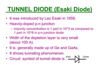
1. TUNNEL DIODE (Esaki Diode)
• It was introduced by Leo Esaki in 1958.
• Heavily-doped p-n junction
– Impurity concentration is 1 part in 10^3 as compared to
1 part in 10^8 in p-n junction diode
• Width of the depletion layer is very small
(about 100 A).
• It is generally made up of Ge and GaAs.
• It shows tunneling phenomenon.
• Circuit symbol of tunnel diode is :
EV
2. WHAT IS TUNNELING
• Classically, carrier must have energy at least
equal to potential-barrier height to cross the
junction .
• But according to Quantum mechanics there is
finite probability that it can penetrate through the
barrier for a thin width.
• This phenomenon is
called tunneling and
hence the Esaki Diode
is know as
Tunnel Diode.
3. - Ve Resistance Region
Vf
Vp
Ip
Vv
Forward Voltage
Reverse
voltage
Iv
Reverse
Current
Forward
Current
Ip:- Peak Current
Iv :- Valley Current
Vp:- Peak Voltage
Vv:- Valley Voltage
Vf:- Peak Forward
Voltage
CHARACTERISTIC OF TUNNEL DIODE
4. ENERGY BAND DIAGRAM
Energy-band diagram of pn junction in thermal equilibrium in which both the n
and p region are degenerately doped.
5. -Zero current on the I-V diagram;
-All energy states are filled below EF on both sides of the junction;
AT ZERO BIAS
Simplified energy-band diagram and I-V characteristics of the tunnel diode at zero bias.
6. -Electrons in the conduction band of the n region are directly opposite to
the empty states in the valence band of the p region.
-So a finite probability that some electrons tunnel directly into the empty
states resulting in forward-bias tunneling current.
AT SMALL FORWARD VOLTAGE
Simplified energy-band diagram and I-V characteristics of the tunnel diode at a slight forward bias.
7. -The maximum number of electrons in the n region are opposite to the
maximum number of empty states in the p region.
- Hence tunneling current is maximum.
AT MAXIMUM TUNNELING CURENT
Simplified energy-band diagraam and I-V characteristics of the tunnel diode at a forward bias
producing maximum tunneling current.
8. -The forward-bias voltage increases so the number of electrons on the n side,
directly opposite empty states on the p side decreases.
- Hence the tunneling current decreases.
AT DECREASING CURRENT REGION
Simplified energy-band diagram and I-V characteristics of the tunnel diode at a higher forward
bias producing less tunneling current.
9. -No electrons on the n side are directly opposite to the empty
states on the p side.
- The tunneling current is zero.
-The normal ideal diffusion current exists in the device.
AT HIGHER FORWARD VOLTAGE
Simplified energy-band diagram and I-V characteristics of the tunnel diode at a forward bias
for which the diffusion current dominates.
10. - Electrons in the valence band on the p side are directly opposite to
empty states in the conduction band on the n side.
-Electrons tunnel directly from the p region into the n region.
- The reverse-bias current increases monotonically and rapidly with
reverse-bias voltage.
AT REVERSE BIAS VOLTAGE
11. Cj -R
rs
Ls
TUNNEL DIODE EQUIVALENT CIRCUIT
•This is the equivalent
circuit of tunnel diode
when biased in negative
resistance region.
•At higher frequencies the
series R and L can be
ignored.
•Hence equivalent circuit can be reduced to parallel
combination of junction capacitance and negative
resistance.