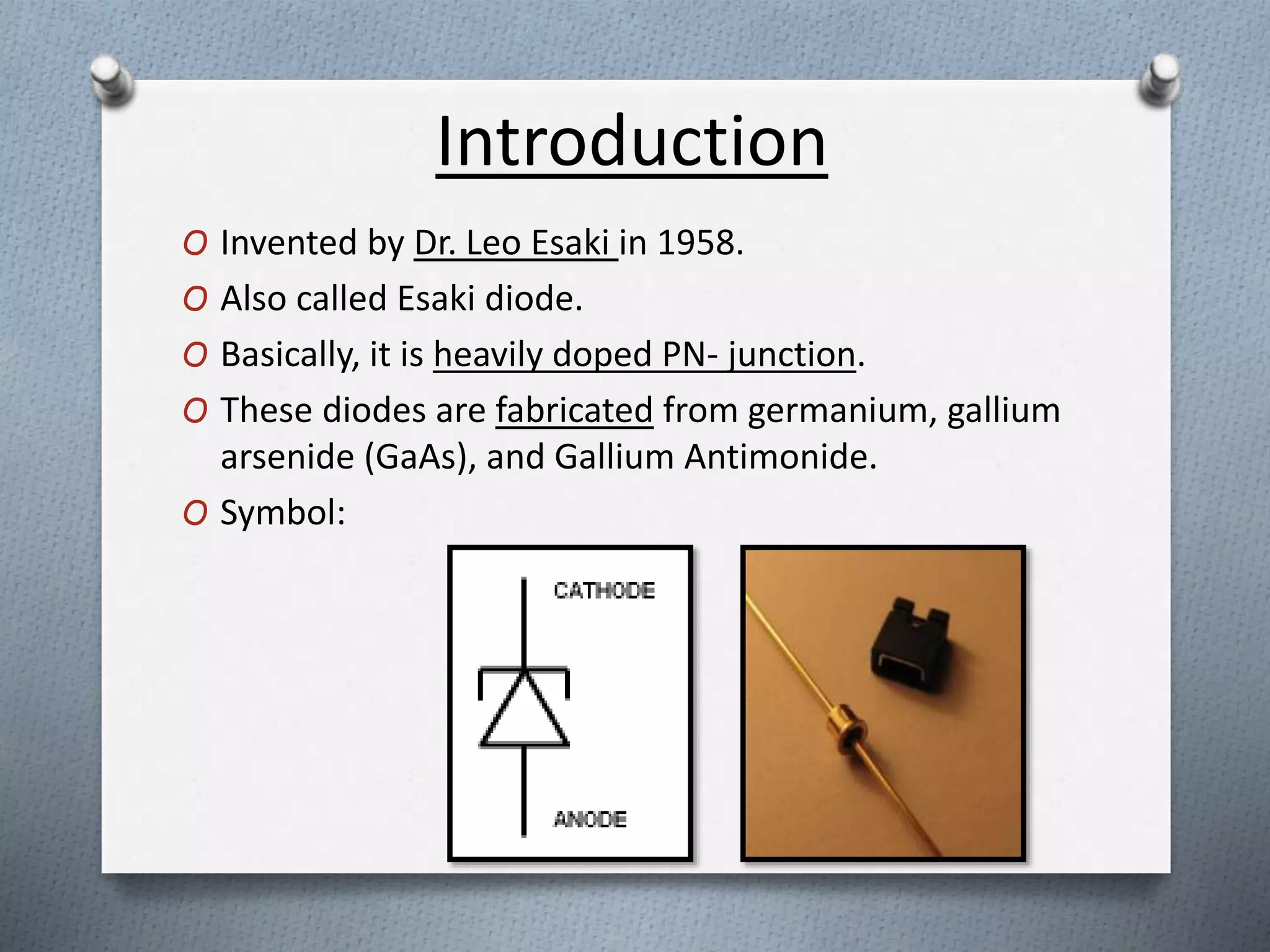
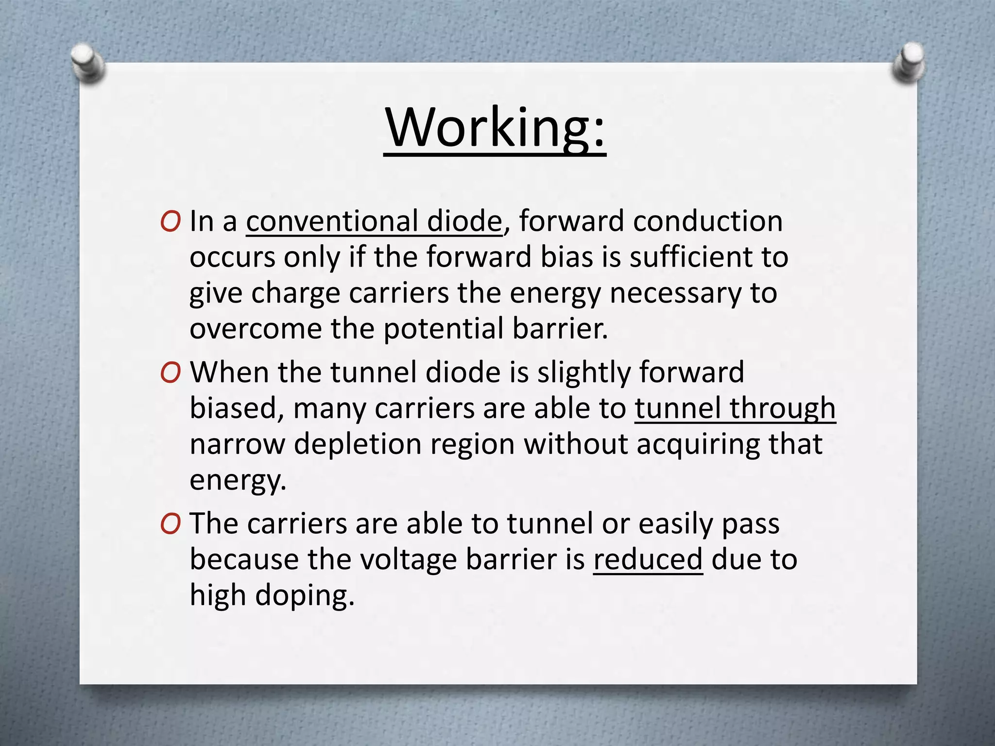
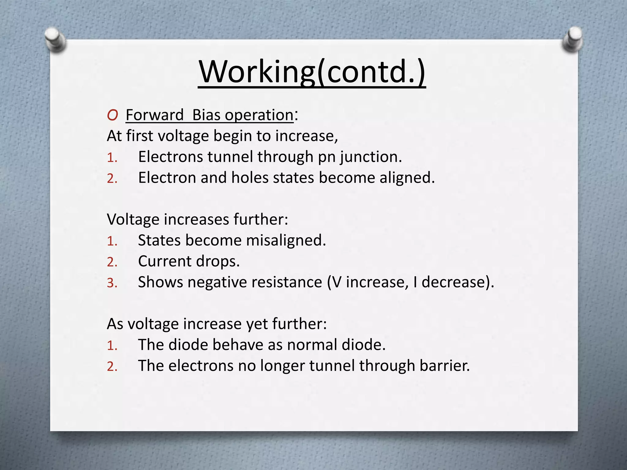
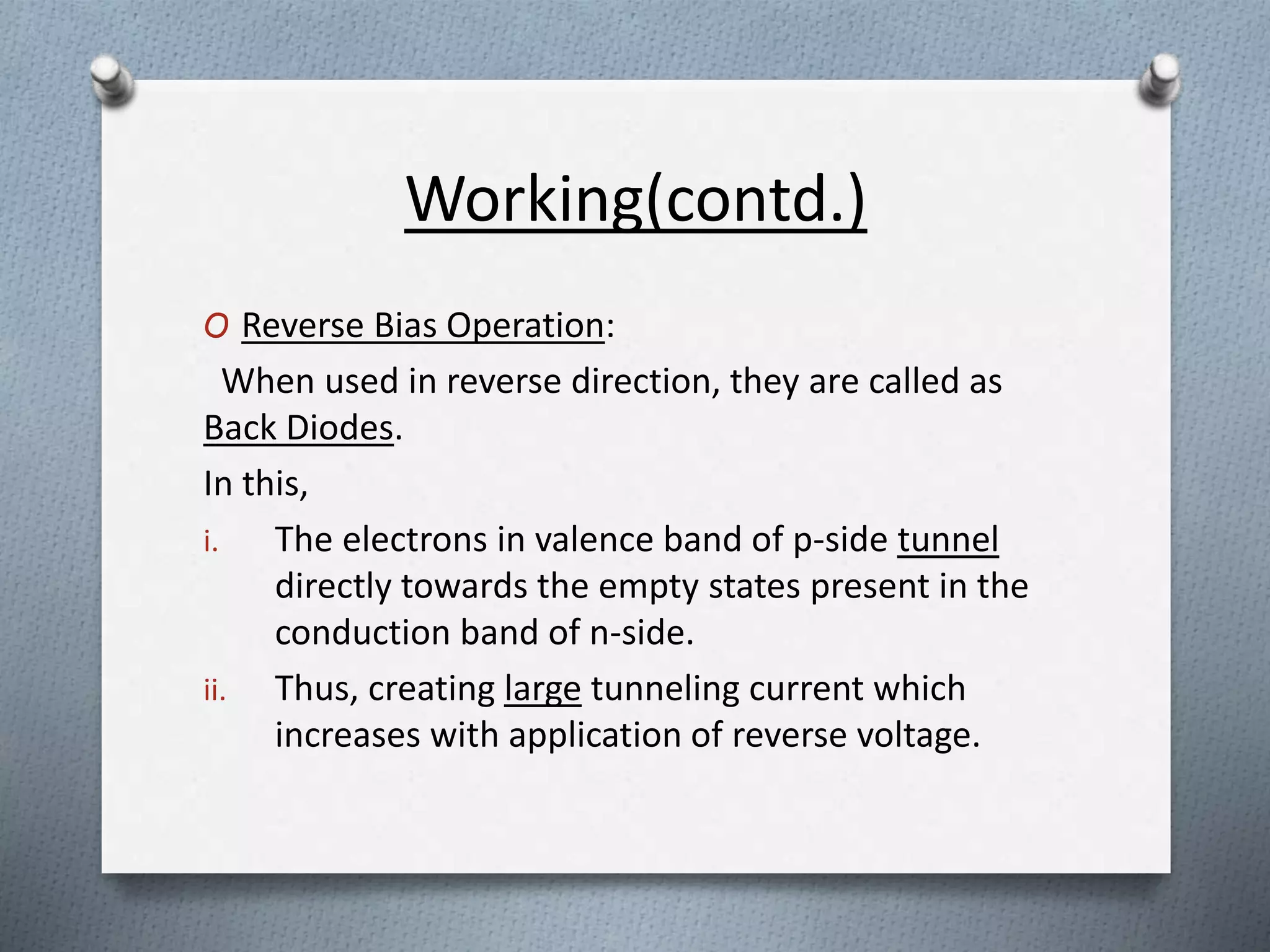
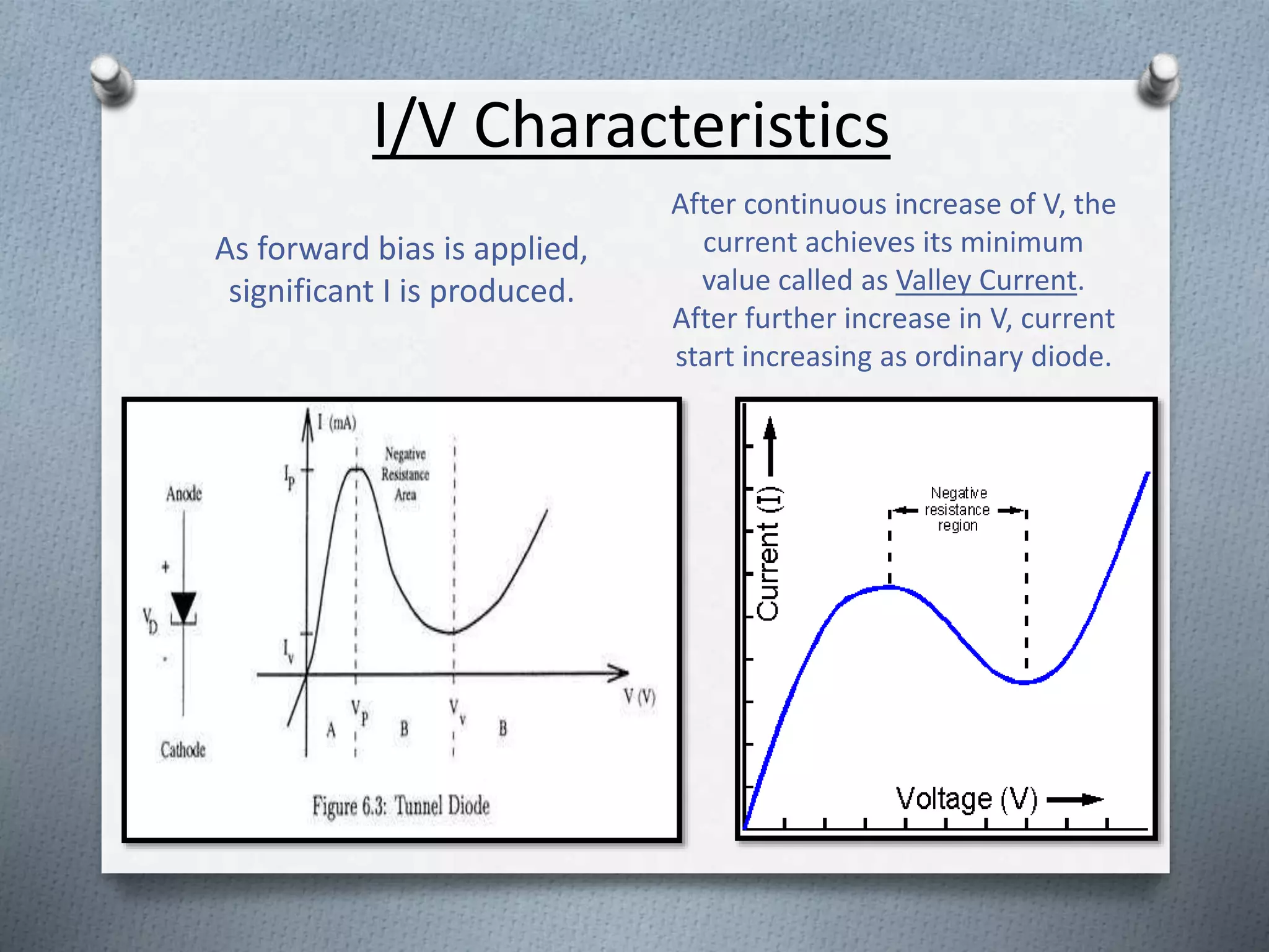
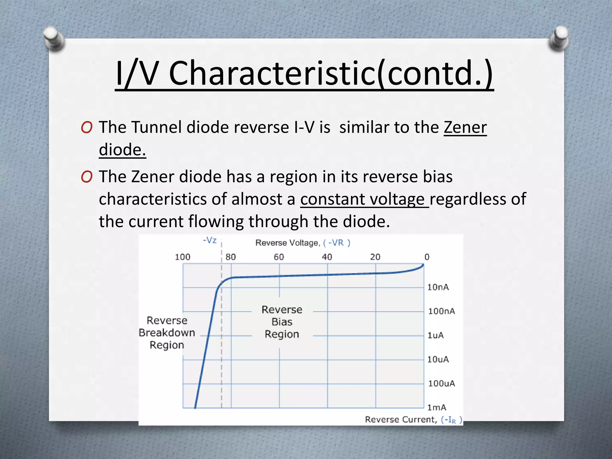
Introduction
O Invented by Dr. Leo Esaki in 1958.
O Also called Esaki diode.
O Basically, it is heavily doped PN- junction.
O These diodes are fabricated from germanium, gallium
arsenide (GaAs), and Gallium Antimonide.
O Symbol:
Description
O Tunnel diode is a semi-conductor with a
special characteristic of negative resistance.
O By negative resistance, we mean that when
voltage is increased, the current through it
decreases.
O Highly doped PN- junction. Doping density of
about 1000 times greater than ordinary
junction diode.
Construction
O Heavy Doping Effects:
i. Reduces the width of depletion layer to about
0.00001 mm.
ii. Produces negative resistance section in
characteristics graph of diode.
iii. Reduces the reverse breakdown voltage
to a small value approaches to zero.
iv. Small forbidden gaps in tunnel diode.
v. Allows conduction for all reverse voltages.
Basic principle of operation:
O The operation depends upon quantum mechanics
principle known as “tunneling”.
O The movement of valence electrons from valence
energy band to conduction band with no applied
forward voltage is called “tunneling”.
O Intrinsic voltage barrier (0.3V for Ge) is reduced
which enhanced tunneling.
O Enhanced tunneling causes effective conductivity.
Working:
O In a conventional diode, forward conduction
occurs only if the forward bias is sufficient to
give charge carriers the energy necessary to
overcome the potential barrier.
O When the tunnel diode is slightly forward
biased, many carriers are able to tunnel through
narrow depletion region without acquiring that
energy.
O The carriers are able to tunnel or easily pass
because the voltage barrier is reduced due to
high doping.
Working(contd.)
O Forward Bias operation:
At first voltage begin to increase,
1. Electrons tunnel through pn junction.
2. Electron and holes states become aligned.
Voltage increases further:
1. States become misaligned.
2. Current drops.
3. Shows negative resistance (V increase, I decrease).
As voltage increase yet further:
1. The diode behave as normal diode.
2. The electrons no longer tunnel through barrier.
Working(contd.)
O Reverse Bias Operation:
When used in reverse direction, they are called as
Back Diodes.
In this,
i. The electrons in valence band of p-side tunnel
directly towards the empty states present in the
conduction band of n-side.
ii. Thus, creating large tunneling current which
increases with application of reverse voltage.
I/V Characteristics
As forward bias is applied,
significant I is produced.
After continuous increase of V, the
current achieves its minimum
value called as Valley Current.
After further increase in V, current
start increasing as ordinary diode.
I/V Characteristic(contd.)
O The Tunnel diode reverse I-V is similar to the Zener
diode.
O The Zener diode has a region in its reverse bias
characteristics of almost a constant voltage regardless of
the current flowing through the diode.
Applications:
O It is used as an ultra- high speed switch due to
tunneling (which essentially takes place at speed of
light). It has switching time of nanoseconds or
picoseconds.
O Used as logic memory storage device.
O In satellite communication equipment, they are widely
used.
O Due to its feature of –ive resistance, it is used in
relaxation oscillator circuits.
Applications(contd.):
O Tunnel diodes are resistant to the effects of magnetic
fields, high temperature and radioactivity. That’s why
these can be used in modern military equipments -
NMR machines.
O Due to low power requirement, they are used in FM
receivers.

tunneldiode.pptx

  • 1.
    Introduction O Invented byDr. Leo Esaki in 1958. O Also called Esaki diode. O Basically, it is heavily doped PN- junction. O These diodes are fabricated from germanium, gallium arsenide (GaAs), and Gallium Antimonide. O Symbol:
  • 2.
    Description O Tunnel diodeis a semi-conductor with a special characteristic of negative resistance. O By negative resistance, we mean that when voltage is increased, the current through it decreases. O Highly doped PN- junction. Doping density of about 1000 times greater than ordinary junction diode.
  • 3.
    Construction O Heavy DopingEffects: i. Reduces the width of depletion layer to about 0.00001 mm. ii. Produces negative resistance section in characteristics graph of diode. iii. Reduces the reverse breakdown voltage to a small value approaches to zero. iv. Small forbidden gaps in tunnel diode. v. Allows conduction for all reverse voltages.
  • 4.
    Basic principle ofoperation: O The operation depends upon quantum mechanics principle known as “tunneling”. O The movement of valence electrons from valence energy band to conduction band with no applied forward voltage is called “tunneling”. O Intrinsic voltage barrier (0.3V for Ge) is reduced which enhanced tunneling. O Enhanced tunneling causes effective conductivity.
  • 5.
    Working: O In aconventional diode, forward conduction occurs only if the forward bias is sufficient to give charge carriers the energy necessary to overcome the potential barrier. O When the tunnel diode is slightly forward biased, many carriers are able to tunnel through narrow depletion region without acquiring that energy. O The carriers are able to tunnel or easily pass because the voltage barrier is reduced due to high doping.
  • 6.
    Working(contd.) O Forward Biasoperation: At first voltage begin to increase, 1. Electrons tunnel through pn junction. 2. Electron and holes states become aligned. Voltage increases further: 1. States become misaligned. 2. Current drops. 3. Shows negative resistance (V increase, I decrease). As voltage increase yet further: 1. The diode behave as normal diode. 2. The electrons no longer tunnel through barrier.
  • 7.
    Working(contd.) O Reverse BiasOperation: When used in reverse direction, they are called as Back Diodes. In this, i. The electrons in valence band of p-side tunnel directly towards the empty states present in the conduction band of n-side. ii. Thus, creating large tunneling current which increases with application of reverse voltage.
  • 8.
    I/V Characteristics As forwardbias is applied, significant I is produced. After continuous increase of V, the current achieves its minimum value called as Valley Current. After further increase in V, current start increasing as ordinary diode.
  • 9.
    I/V Characteristic(contd.) O TheTunnel diode reverse I-V is similar to the Zener diode. O The Zener diode has a region in its reverse bias characteristics of almost a constant voltage regardless of the current flowing through the diode.
  • 10.
    Applications: O It isused as an ultra- high speed switch due to tunneling (which essentially takes place at speed of light). It has switching time of nanoseconds or picoseconds. O Used as logic memory storage device. O In satellite communication equipment, they are widely used. O Due to its feature of –ive resistance, it is used in relaxation oscillator circuits.
  • 11.
    Applications(contd.): O Tunnel diodesare resistant to the effects of magnetic fields, high temperature and radioactivity. That’s why these can be used in modern military equipments - NMR machines. O Due to low power requirement, they are used in FM receivers.