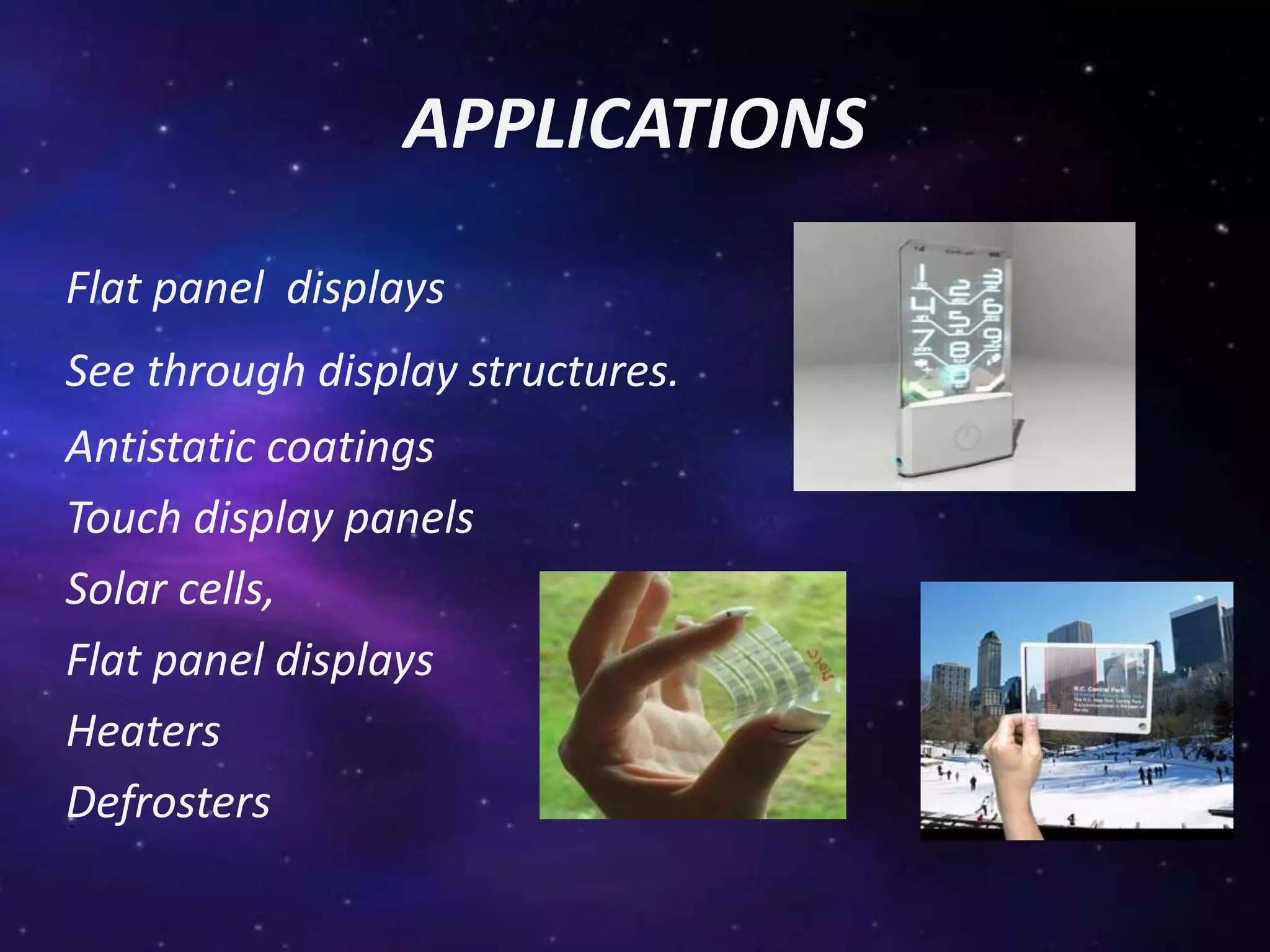
T SRIRAM REDDY
Transparentelectronicsis an emergingtechnology
that employs wide band-gap semiconductors for the
realization of invisiblecircuits.
The scientific goal of this technology must be to
discover, understand, and implement
transparent high-performance electronic
materials and evaluation in transistor and circuit
structures.
INTRODUCTION
The two technologies which preceded and underlined
transparent electronics are :-
a)Transparent Conductive Oxides (TCOs) and
b) Thin- Film Transistors (TFTs).
TCOs constitute an unusual class of materials possessing
two contradictory physical properties-high optical
transparency and high electrical conductivity.
The three most common TCOs are indium oxide (In2O3),
tin oxide (SnO2) and zinc oxide (ZnO2).
COMPONENTS
The thin-film transistor (TFTs) is another technology
underlying transparent electronics, since it is a bridge
between passive electrical and active electronic
applications. But it does not evolve a fully transparent
transistor.
KEY ROLE OF OXIDES
The fact that is possible to growth at/near the room
temperature high quality polycrystalline ZnO, which is a
particular advantage for electronic drivers, where the
response speed is of major importance.
Since ZnO is a wide band gap material (3.4eV), it is
transparent in the visible region of the spectra and
therefore, also less light sensitive.
Active Intrinsic ZnO
The second is amorphous oxides with heavy metal
content, such as amorphous InGaZnO4 (a-IGZO) also
used in this application.
A comparison of ZnO and a-IGZO shows that ZnO has
the lead when it comes carrier mobility. At present
though , a–IGZO is a material of choice of large area
displays , electronic paper utilizing low temperature
processing ,etc.
a-IGZO
The major substrate used for this purpose is Glass.
Less Size and Weight
Recyclable
Low cost
Easy fabrication
Wide viewing angle
Low temperature processing
ADVANTAGES
DISADVANTAGES
Lifetime is less when compared to non-transparent
electronic devices i.e.,
Red and Green OLEDs – 46,000 to 230,000 hours
Blue organics – around 14,000 hours
Manufacturing processes are expensive
Water can easily damage
Flat panel displays
See through display structures.
Antistatic coatings
Touch display panels
Solar cells,
Flat panel displays
Heaters
Defrosters
APPLICATIONS
FUTURE SCOPE
In the field of solar cells, although
much progress has been made in
developing new materials and
devices for high performance
transparent solar cells, there is still
plenty of opportunity to study and
improve device performance and
fabrication techniques compared
with the non-transparent solar cell
devices.
Transparent electronics

Transparent electronics

  • 1.
  • 2.
    Transparentelectronicsis an emergingtechnology thatemploys wide band-gap semiconductors for the realization of invisiblecircuits. The scientific goal of this technology must be to discover, understand, and implement transparent high-performance electronic materials and evaluation in transistor and circuit structures. INTRODUCTION
  • 5.
    The two technologieswhich preceded and underlined transparent electronics are :- a)Transparent Conductive Oxides (TCOs) and b) Thin- Film Transistors (TFTs). TCOs constitute an unusual class of materials possessing two contradictory physical properties-high optical transparency and high electrical conductivity. The three most common TCOs are indium oxide (In2O3), tin oxide (SnO2) and zinc oxide (ZnO2). COMPONENTS
  • 6.
    The thin-film transistor(TFTs) is another technology underlying transparent electronics, since it is a bridge between passive electrical and active electronic applications. But it does not evolve a fully transparent transistor.
  • 7.
    KEY ROLE OFOXIDES The fact that is possible to growth at/near the room temperature high quality polycrystalline ZnO, which is a particular advantage for electronic drivers, where the response speed is of major importance. Since ZnO is a wide band gap material (3.4eV), it is transparent in the visible region of the spectra and therefore, also less light sensitive. Active Intrinsic ZnO
  • 8.
    The second isamorphous oxides with heavy metal content, such as amorphous InGaZnO4 (a-IGZO) also used in this application. A comparison of ZnO and a-IGZO shows that ZnO has the lead when it comes carrier mobility. At present though , a–IGZO is a material of choice of large area displays , electronic paper utilizing low temperature processing ,etc. a-IGZO The major substrate used for this purpose is Glass.
  • 9.
    Less Size andWeight Recyclable Low cost Easy fabrication Wide viewing angle Low temperature processing ADVANTAGES
  • 10.
    DISADVANTAGES Lifetime is lesswhen compared to non-transparent electronic devices i.e., Red and Green OLEDs – 46,000 to 230,000 hours Blue organics – around 14,000 hours Manufacturing processes are expensive Water can easily damage
  • 11.
    Flat panel displays Seethrough display structures. Antistatic coatings Touch display panels Solar cells, Flat panel displays Heaters Defrosters APPLICATIONS
  • 12.
    FUTURE SCOPE In thefield of solar cells, although much progress has been made in developing new materials and devices for high performance transparent solar cells, there is still plenty of opportunity to study and improve device performance and fabrication techniques compared with the non-transparent solar cell devices.