Submitted by-
REHAN FAZAL
1171110180
Electronics and Instrumentation
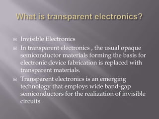
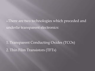
 Researchers at Oregon State University have
reported their first example of an entirely new
class of materials which could be used to make
transparent transistors that are inexpensive, stable,
and eco-friendly. This could lead to new industries
and a broad range of new consumer products, The
possibilities include electronic devices produced so
cheaply they could almost be one-time "throw
away" products, better large-area electronics such
as flat panel screens, or flexible electronics that
could be folded up for ease of transport. Findings
about this new class of "thin-film" materials are
called amorphous heavy-metal cation
multicomponent oxides.
 Invisible Electronics
 In transparent electronics , the usual opaque
semiconductor materials forming the basis for
electronic device fabrication is replaced with
transparent materials.
 Transparent electronics is an emerging
technology that employs wide band-gap
semiconductors for the realization of invisible
circuits
There are two technologies which preceded and
underlie transparent electronics:
1. Transparent Conducting Oxides (TCOs)
2. Thin Film Transistors (TFTs)
TCOs constitute an unusual class of materials
possessing two physical properties (generally
considered mutually exclusive):
1. High optical transparency. ( E.g.>3.1eV)
2. High electrical conductivity.
Transparent electronic
devices
Transparent Passive devices
Transparent Active devices
 Constitutes the heart of transparent electronics
 Channel is formed from highly insulating, wide
band gap transparent semiconductor(ZnO).
 Source, drain and gate contacts are made from
highly conductive TCO (ITO).
 Two possible configurations are:
a) Bottom gate
b) Top gate
Possible structure, (a) Bottom gate, and
(b) Top gate.
 Significant advances in the emerging science of
transparent electronics, creating transparent "p-type"
semiconductors that have more than 200 times the
conductivity of the best materials available for that
purpose a few years ago. This basic research is opening the
door to new types of electronic circuits that, when
deposited onto glass, are literally invisible. These "p-type"
materials will be necessary for the diodes and transistors
that are essential to more complex electronic devices. Only
a few laboratories in the world are working in this
area, mostly in Japan, the OSU scientists. As recently as
1997, the best transparent p-type transparent conductive
materials could only conduct one Siemen/cm, which is a
measure of electrical conductivity. The most sophisticated
materials recently developed at OSU now conduct 220
Siemen/cm.
Strengths Weaknesses
Visible transparency High resistance of TCO’s
Large area Lack of complementary devices
Low cost (solution based deposition
and printing)
Low temperature processing Technological immaturity
Free real estate
Passive availability (R & C)
Robust stable inorganic materials
Safe, nontoxic materials
STRENGTHS AND WEAKNESSES
They have been widely used in a variety of applications
like:
 Active Matrix LCD (AMLCD).
 Active Matrix Organic Light Emitting Device display
backplane (AMOLED).
 Value added glass.
 Transparent electronics on opaque substrates
 UV detectors and arrays
 Transparent solar cells
 UV detectors for spectrally resolved imaging.
 Security applications:
 Invisible cameras and
 Invisible RFID’s

Started as a mere electrical device technology
during world war 2, transparent electronics
now holds the key for many future
advancements in security, entertainment
efficient utilization of energy.
Transparent Electronics

Transparent Electronics

  • 1.
  • 2.
     Researchers atOregon State University have reported their first example of an entirely new class of materials which could be used to make transparent transistors that are inexpensive, stable, and eco-friendly. This could lead to new industries and a broad range of new consumer products, The possibilities include electronic devices produced so cheaply they could almost be one-time "throw away" products, better large-area electronics such as flat panel screens, or flexible electronics that could be folded up for ease of transport. Findings about this new class of "thin-film" materials are called amorphous heavy-metal cation multicomponent oxides.
  • 3.
     Invisible Electronics In transparent electronics , the usual opaque semiconductor materials forming the basis for electronic device fabrication is replaced with transparent materials.  Transparent electronics is an emerging technology that employs wide band-gap semiconductors for the realization of invisible circuits
  • 4.
    There are twotechnologies which preceded and underlie transparent electronics: 1. Transparent Conducting Oxides (TCOs) 2. Thin Film Transistors (TFTs)
  • 5.
    TCOs constitute anunusual class of materials possessing two physical properties (generally considered mutually exclusive): 1. High optical transparency. ( E.g.>3.1eV) 2. High electrical conductivity.
  • 6.
    Transparent electronic devices Transparent Passivedevices Transparent Active devices
  • 7.
     Constitutes theheart of transparent electronics  Channel is formed from highly insulating, wide band gap transparent semiconductor(ZnO).  Source, drain and gate contacts are made from highly conductive TCO (ITO).  Two possible configurations are: a) Bottom gate b) Top gate
  • 8.
    Possible structure, (a)Bottom gate, and (b) Top gate.
  • 11.
     Significant advancesin the emerging science of transparent electronics, creating transparent "p-type" semiconductors that have more than 200 times the conductivity of the best materials available for that purpose a few years ago. This basic research is opening the door to new types of electronic circuits that, when deposited onto glass, are literally invisible. These "p-type" materials will be necessary for the diodes and transistors that are essential to more complex electronic devices. Only a few laboratories in the world are working in this area, mostly in Japan, the OSU scientists. As recently as 1997, the best transparent p-type transparent conductive materials could only conduct one Siemen/cm, which is a measure of electrical conductivity. The most sophisticated materials recently developed at OSU now conduct 220 Siemen/cm.
  • 13.
    Strengths Weaknesses Visible transparencyHigh resistance of TCO’s Large area Lack of complementary devices Low cost (solution based deposition and printing) Low temperature processing Technological immaturity Free real estate Passive availability (R & C) Robust stable inorganic materials Safe, nontoxic materials STRENGTHS AND WEAKNESSES
  • 14.
    They have beenwidely used in a variety of applications like:  Active Matrix LCD (AMLCD).  Active Matrix Organic Light Emitting Device display backplane (AMOLED).  Value added glass.  Transparent electronics on opaque substrates
  • 15.
     UV detectorsand arrays  Transparent solar cells  UV detectors for spectrally resolved imaging.  Security applications:  Invisible cameras and  Invisible RFID’s
  • 16.
     Started as amere electrical device technology during world war 2, transparent electronics now holds the key for many future advancements in security, entertainment efficient utilization of energy.