![( ) [ ( ) ]
D D GS C TO
Q y WC V V y V
= − −
6/7/2021 24
Arpan Deyasi, RCCIIT
I-V Characteristics of MOSFET
Assume 1D carrier flow
Total mobile electron charge in surface
inversion layer (per unit length) is](https://image.slidesharecdn.com/electricalcharacteristicsofmosfet-210607174841/75/Electrical-characteristics-of-MOSFET-24-2048.jpg)
![( )
D D n
I Q y v
= −
[( ( ) ]
D D GS C TO n
I WC V V y V v
=
− − −
6/7/2021 25
Arpan Deyasi, RCCIIT
I-V Characteristics of MOSFET
Current is given by
independent of dimension](https://image.slidesharecdn.com/electricalcharacteristicsofmosfet-210607174841/75/Electrical-characteristics-of-MOSFET-25-2048.jpg)
![n n y
v E
µ
=
( )
n n C
d
v V y
dy
µ
= −
[( ( ) ] ( )
D D GS C TO n C
d
I WC V V y V V y
dy
µ
= − −
6/7/2021 26
Arpan Deyasi, RCCIIT
I-V Characteristics of MOSFET
Velocity of electron
Drain current becomes](https://image.slidesharecdn.com/electricalcharacteristicsofmosfet-210607174841/75/Electrical-characteristics-of-MOSFET-26-2048.jpg)
![[( ( ) ] ( ( ))
D D GS C TO n C
I dy WC V V y V dV y
µ
= − −
0 0
[( ( ) ] ( ( ))
D
V
L
D D GS C TO n C
I dy WC V V y V dV y
µ
= − −
∫ ∫
6/7/2021 27
Arpan Deyasi, RCCIIT
I-V Characteristics of MOSFET](https://image.slidesharecdn.com/electricalcharacteristicsofmosfet-210607174841/75/Electrical-characteristics-of-MOSFET-27-2048.jpg)
![2
1
( )
2
D n D GS TO D D
W
I C V V V V
L
µ
= − −
2
1
[2( ) ]
2
D n D GS TO D D
W
I C V V V V
L
µ − −
6/7/2021 28
Arpan Deyasi, RCCIIT
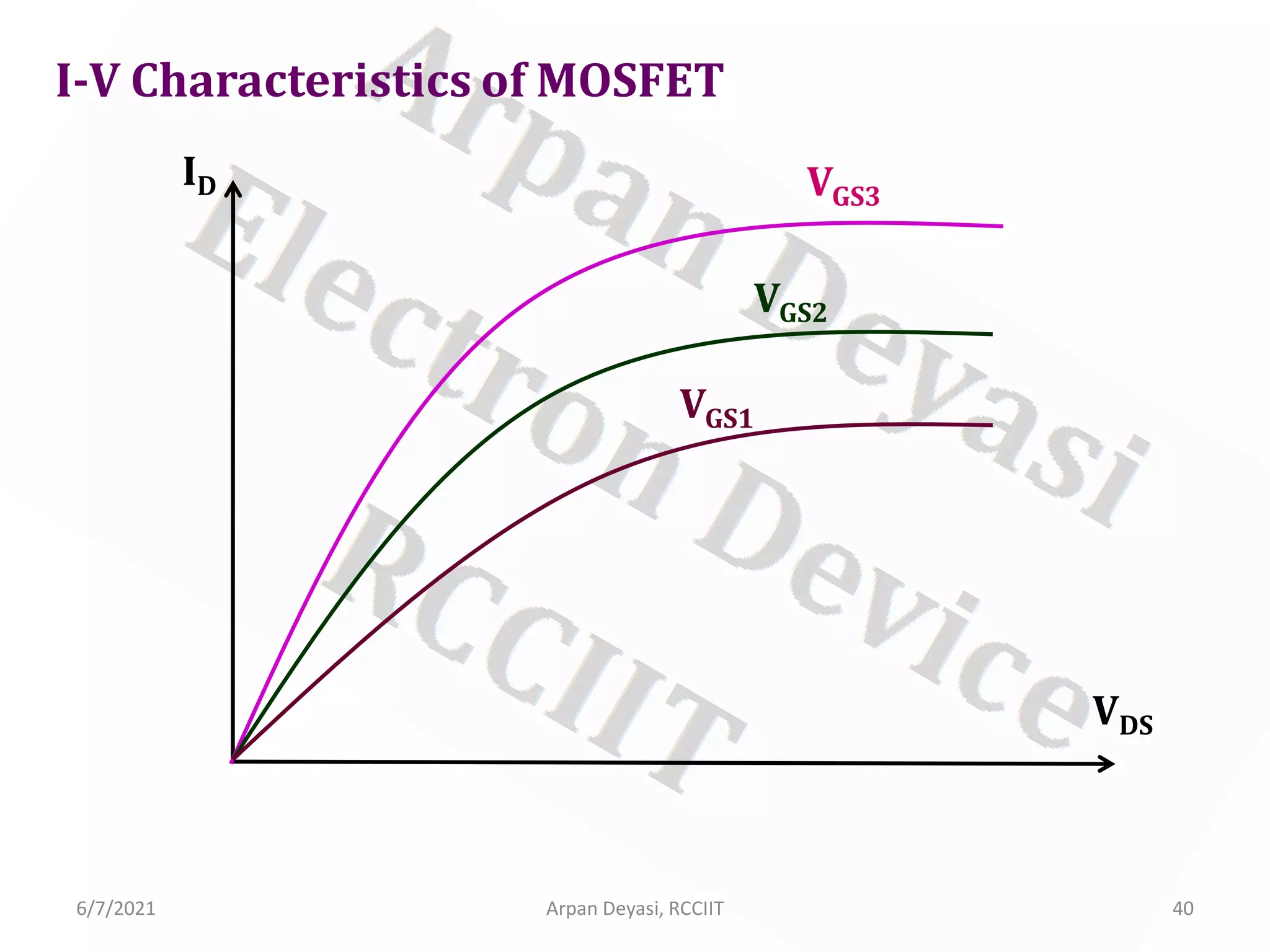
I-V Characteristics of MOSFET
I-V characteristics under active condition](https://image.slidesharecdn.com/electricalcharacteristicsofmosfet-210607174841/75/Electrical-characteristics-of-MOSFET-28-2048.jpg)
![2
1
[2( ) ]
2
D n D GS TO D D
W
I C V V V V
L
µ
= − −
6/7/2021 29
Arpan Deyasi, RCCIIT
I-V Characteristics of MOSFET
β
Q: What is the significance of β?](https://image.slidesharecdn.com/electricalcharacteristicsofmosfet-210607174841/75/Electrical-characteristics-of-MOSFET-29-2048.jpg)
![6/7/2021 Arpan Deyasi, RCCIIT 30
I-V Characteristics of MOSFET
For
( )
D GS TO
V V V
< −
1
[2( ) ]
2
D n D GS TO D
W
I C V V V
L
µ −
D D
I V
∝](https://image.slidesharecdn.com/electricalcharacteristicsofmosfet-210607174841/75/Electrical-characteristics-of-MOSFET-30-2048.jpg)


![6/7/2021 33
Arpan Deyasi, RCCIIT
I-V Characteristics of MOSFET
At peak point
D GS TO
V V V
= −
2
1
[( ) ]
2
DP n D GS TO
W
I C V V
L
µ −](https://image.slidesharecdn.com/electricalcharacteristicsofmosfet-210607174841/75/Electrical-characteristics-of-MOSFET-33-2048.jpg)

![6/7/2021 35
Arpan Deyasi, RCCIIT
I-V Characteristics of MOSFET
Effect of channel length modulation
2
1
[( ) ]
2 '
DS n D GS TO
W
I C V V
L
µ −
2
1
[( ) ]
2
DS n D GS TO
W
I C V V
L L
µ −
− ∆](https://image.slidesharecdn.com/electricalcharacteristicsofmosfet-210607174841/75/Electrical-characteristics-of-MOSFET-35-2048.jpg)
![6/7/2021 36
Arpan Deyasi, RCCIIT
I-V Characteristics of MOSFET
Effect of channel length modulation
2
1
[( ) ]
2
DS n D GS TO
W L
I C V V
L L L
µ
−
− ∆
DS D
L
I I
L L
=
− ∆
](https://image.slidesharecdn.com/electricalcharacteristicsofmosfet-210607174841/75/Electrical-characteristics-of-MOSFET-36-2048.jpg)


2
DS n D GS TO DS
W
I C V V V
L
µ λ
− +
I-V characteristics under saturation condition](https://image.slidesharecdn.com/electricalcharacteristicsofmosfet-210607174841/75/Electrical-characteristics-of-MOSFET-39-2048.jpg)

This document summarizes the electrical characteristics of n-channel MOSFETs. It describes the minority carrier concentration in the depletion region and how the depletion width changes with applied gate voltage. It then discusses the threshold voltage expression and how the threshold is affected by factors like bulk charge, fixed oxide charge and work function differences. Finally, it derives the drain current equation and shows how the I-V characteristics are affected by channel length modulation under different regions of operation.