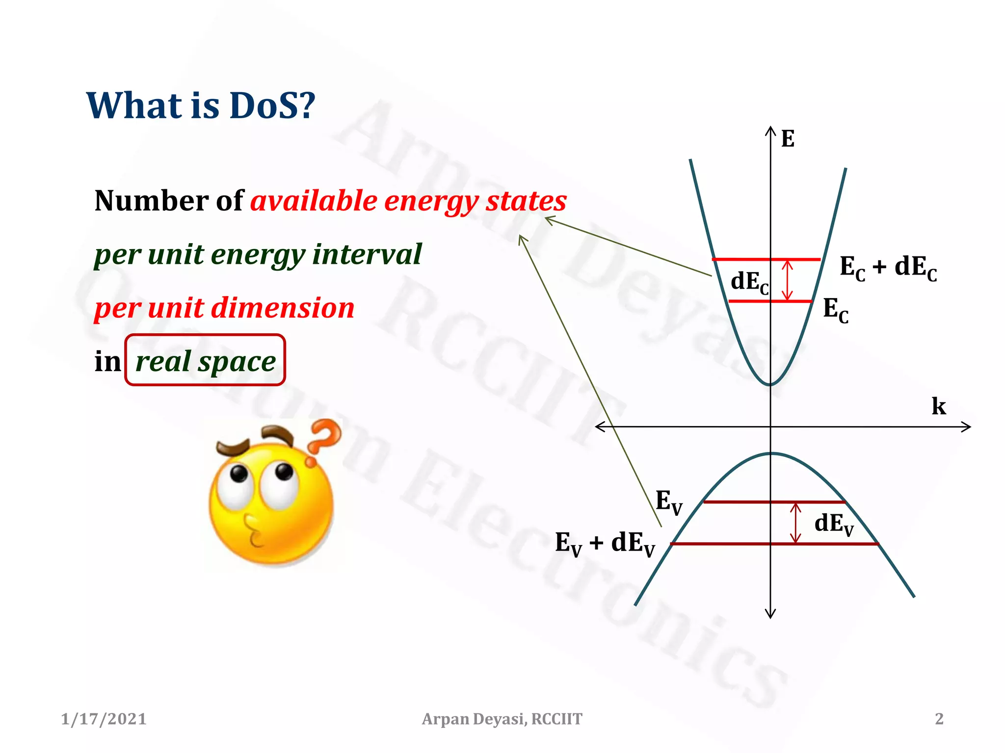
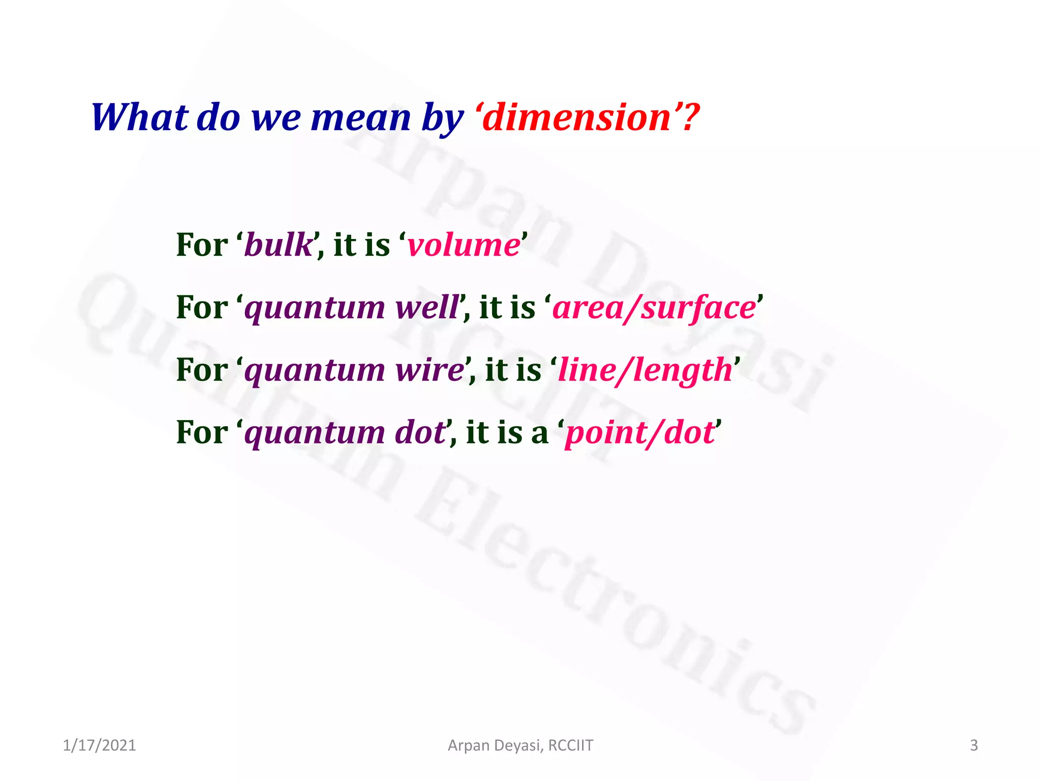
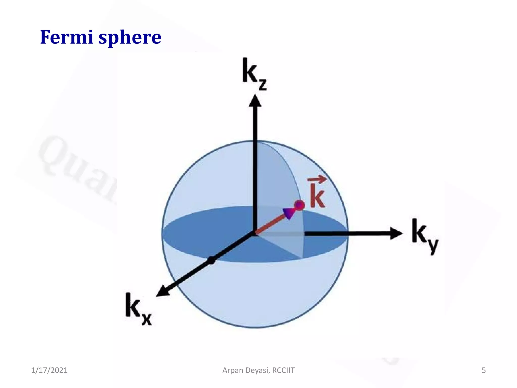
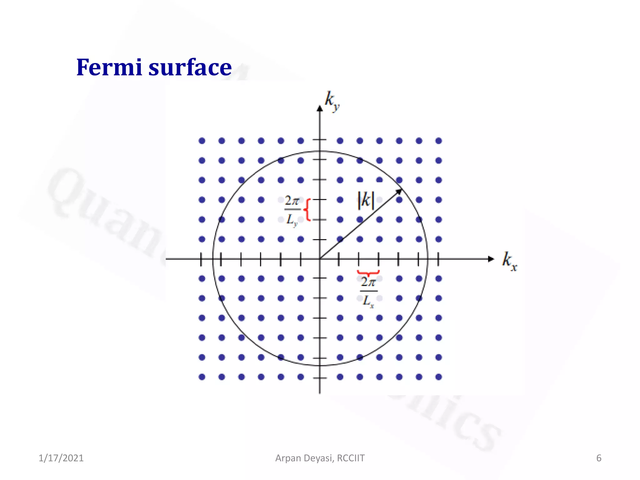
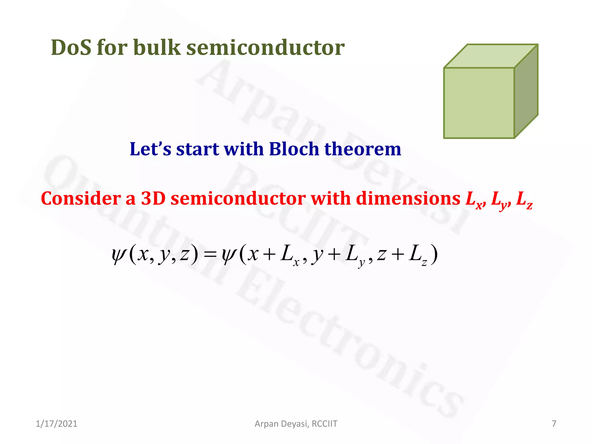
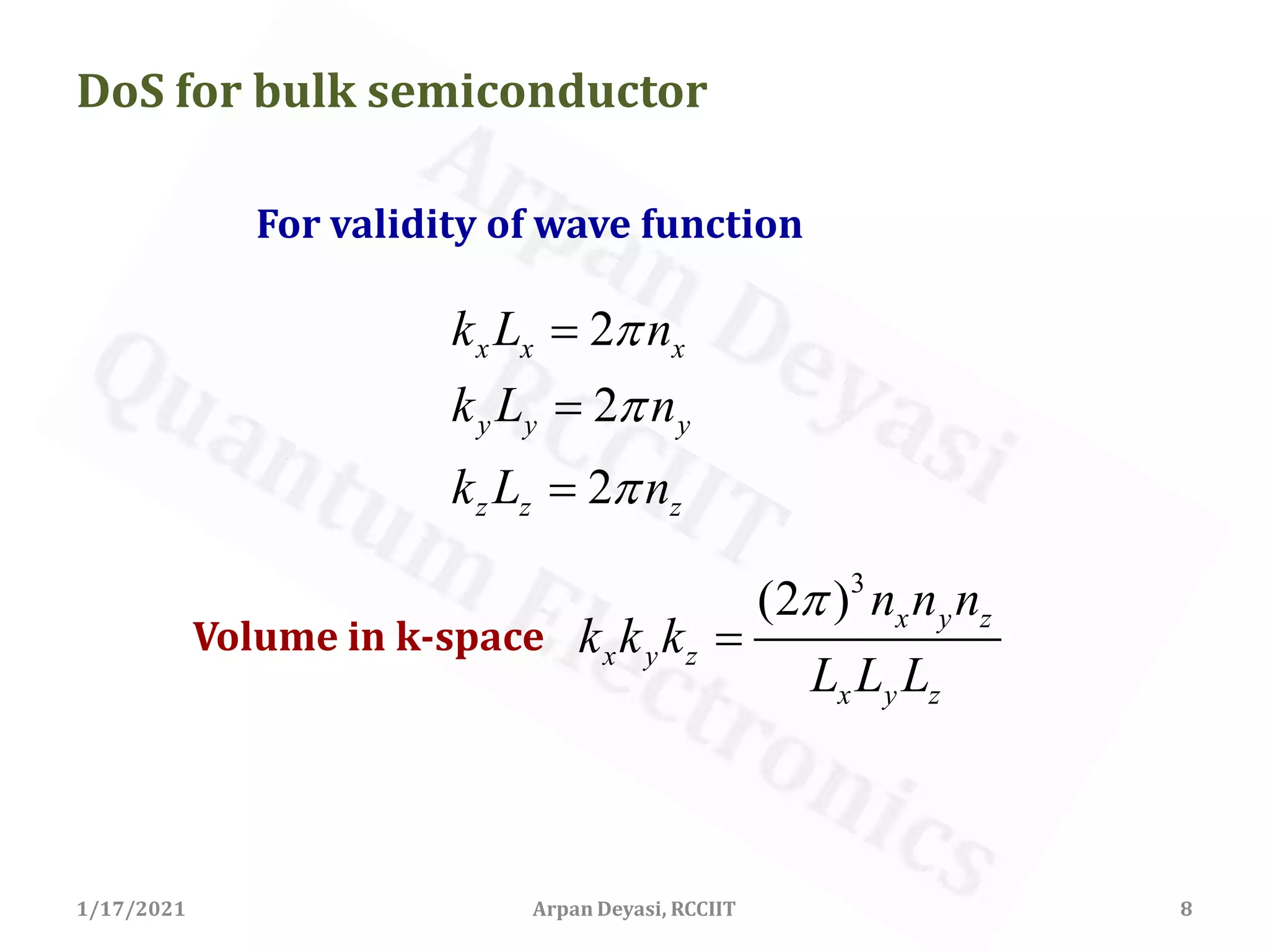
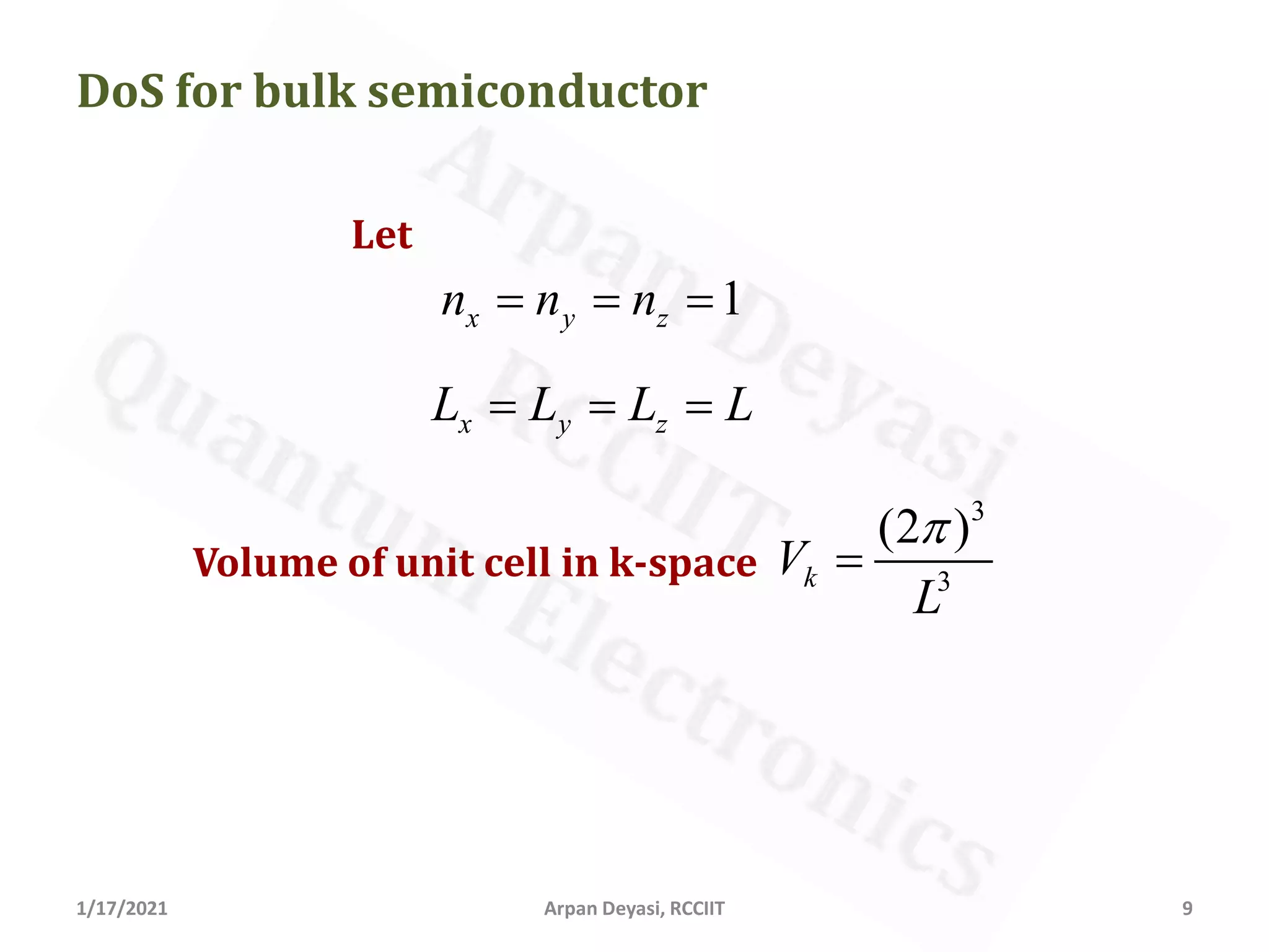
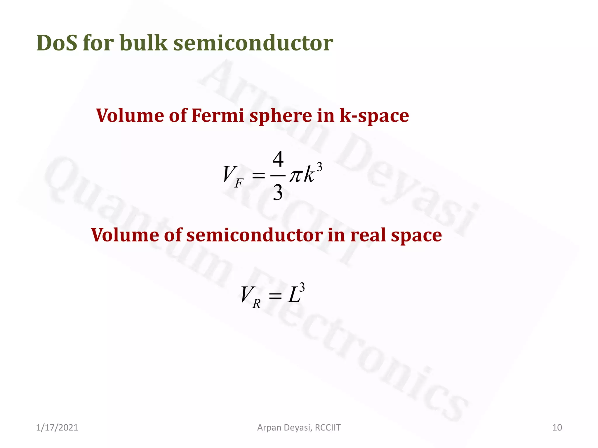
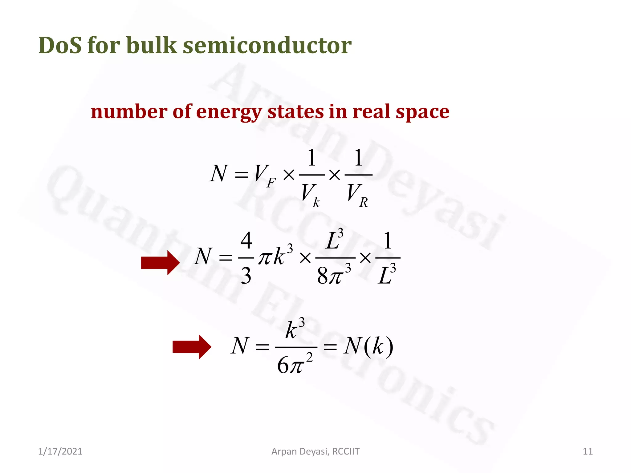
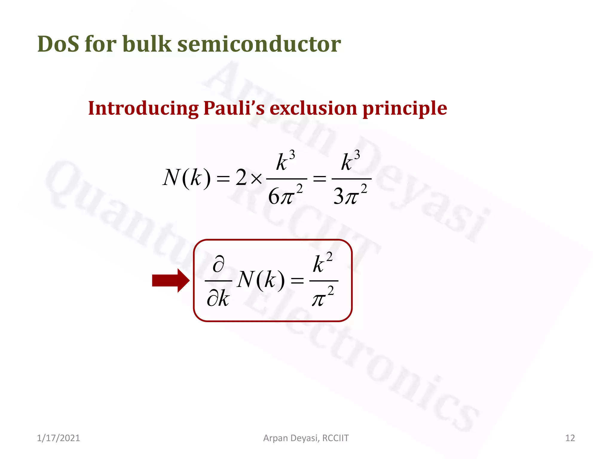
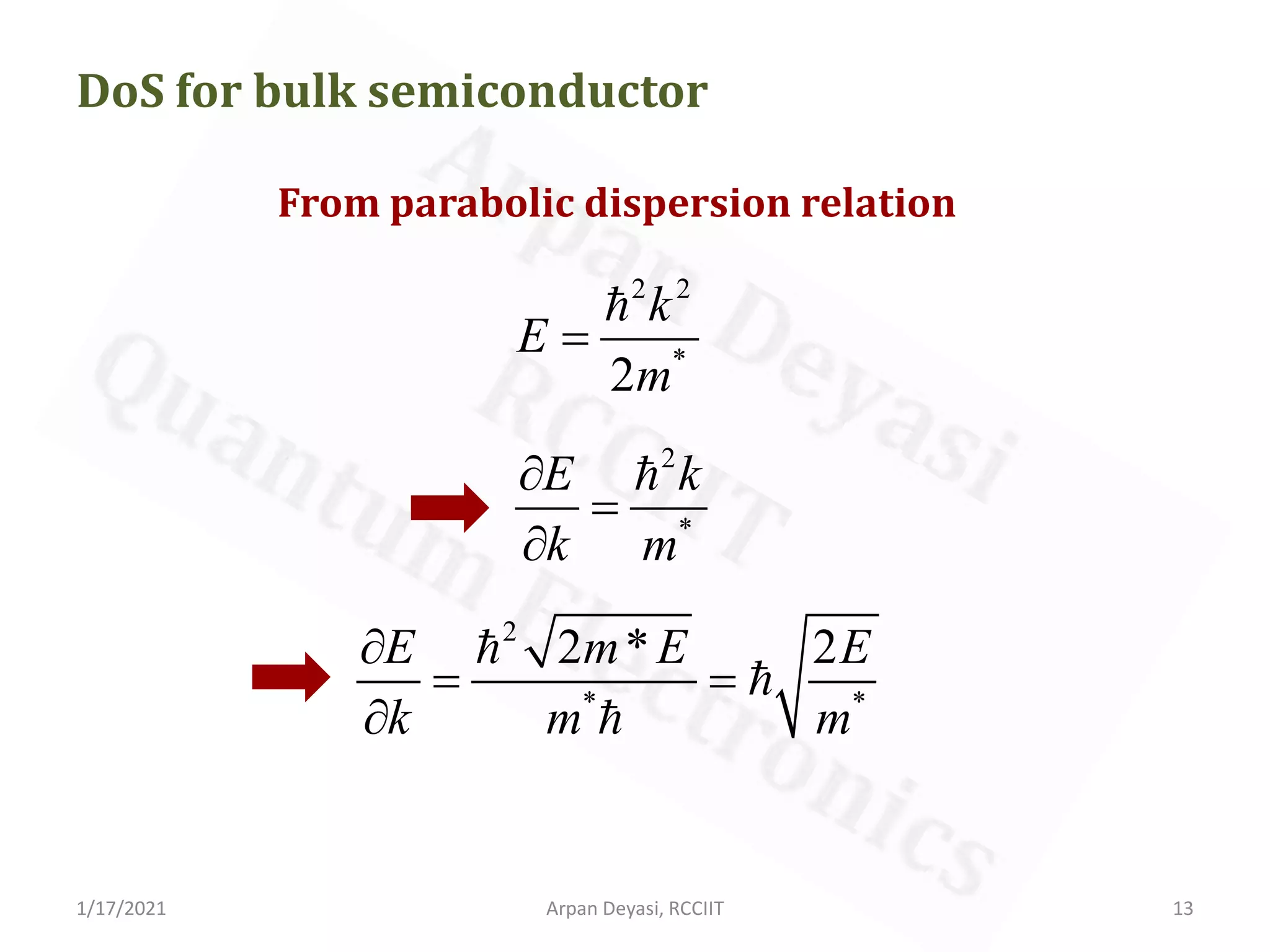
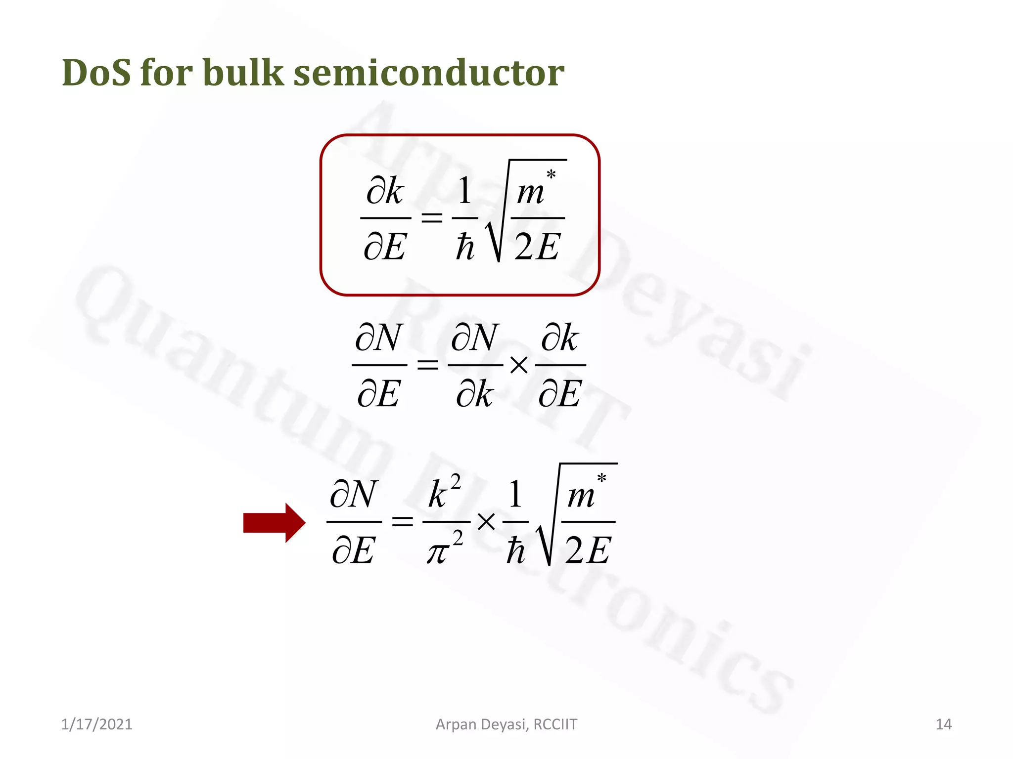
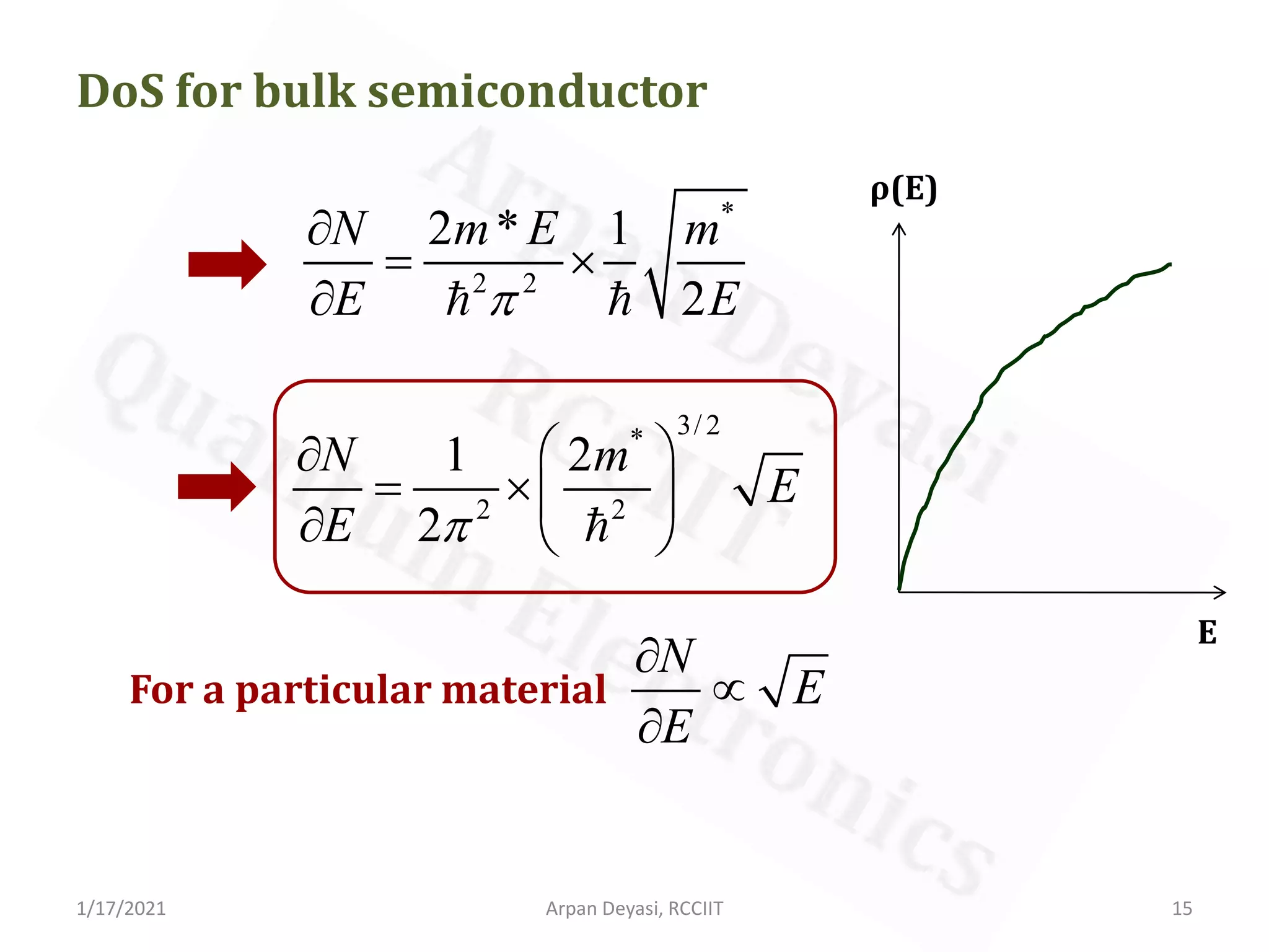
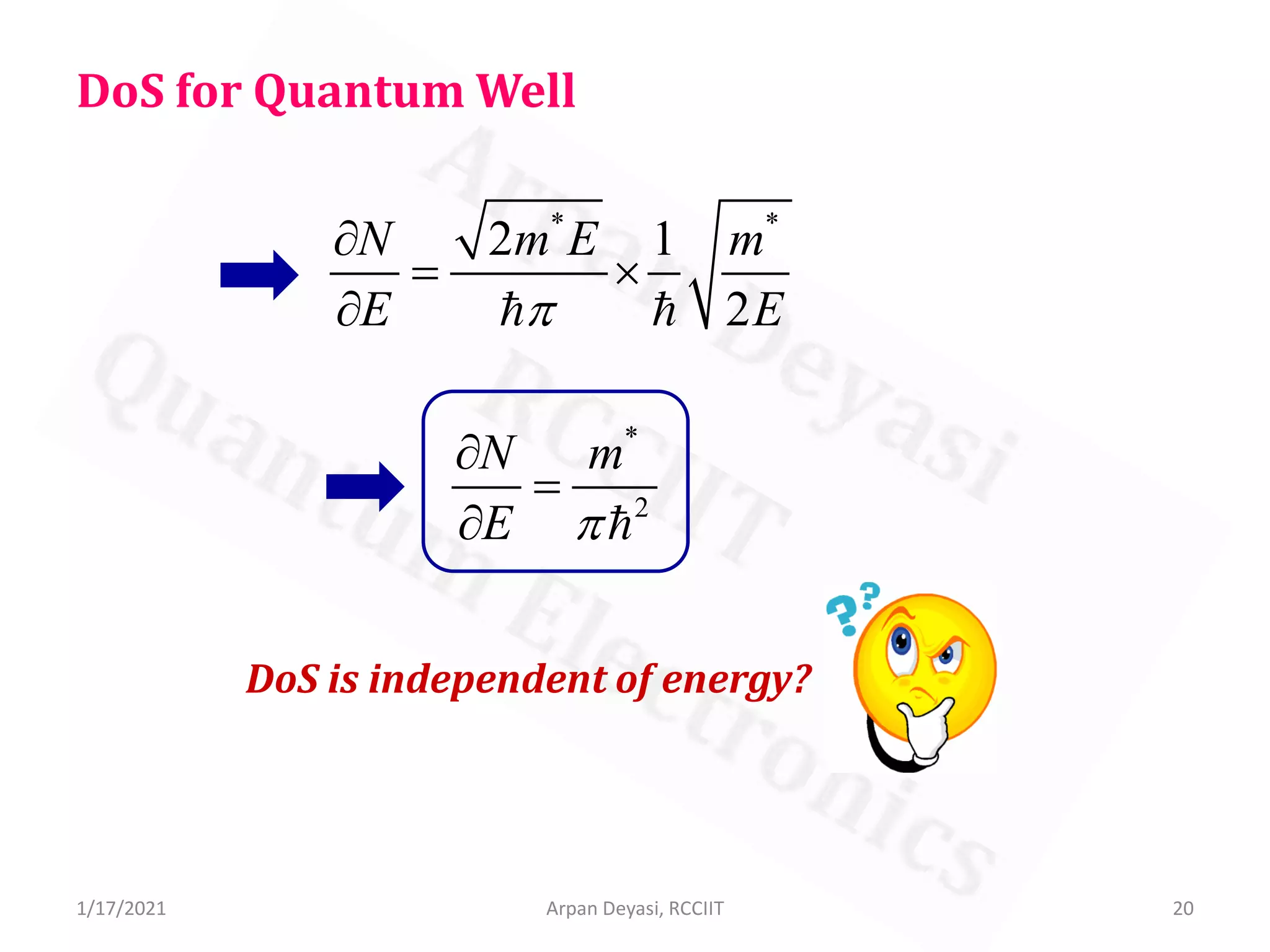
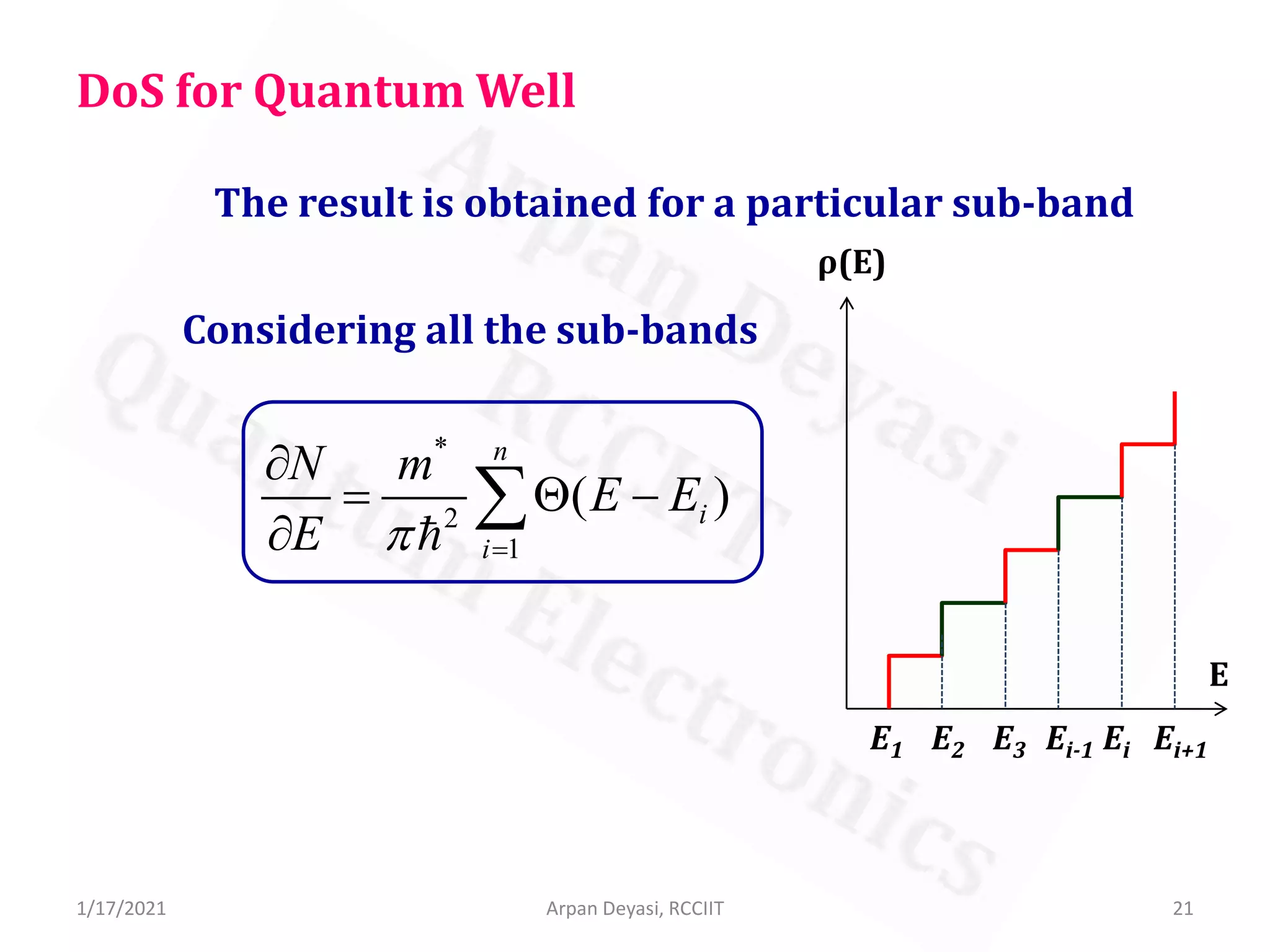
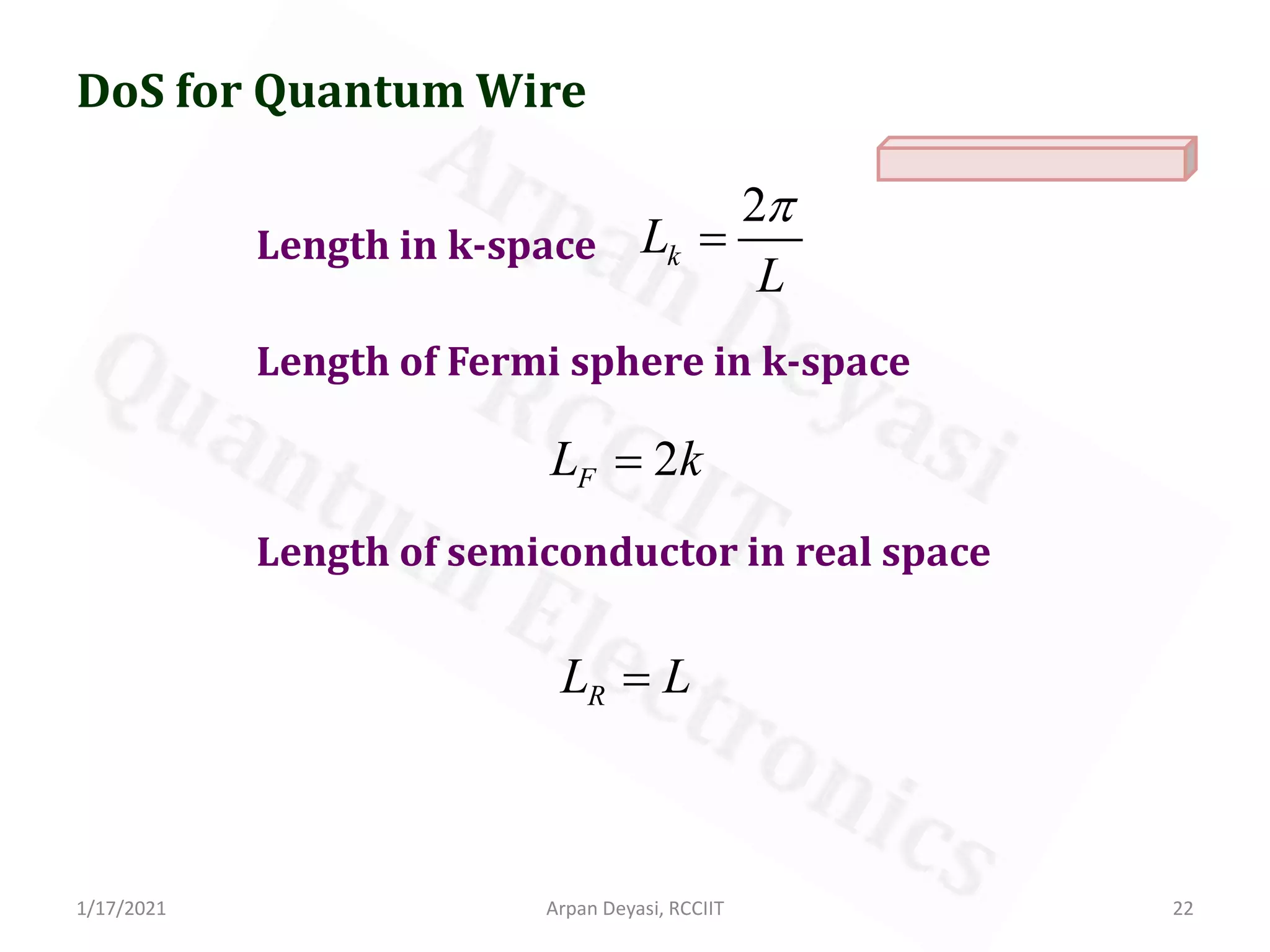
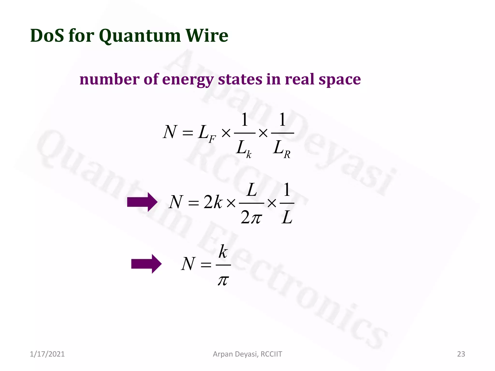
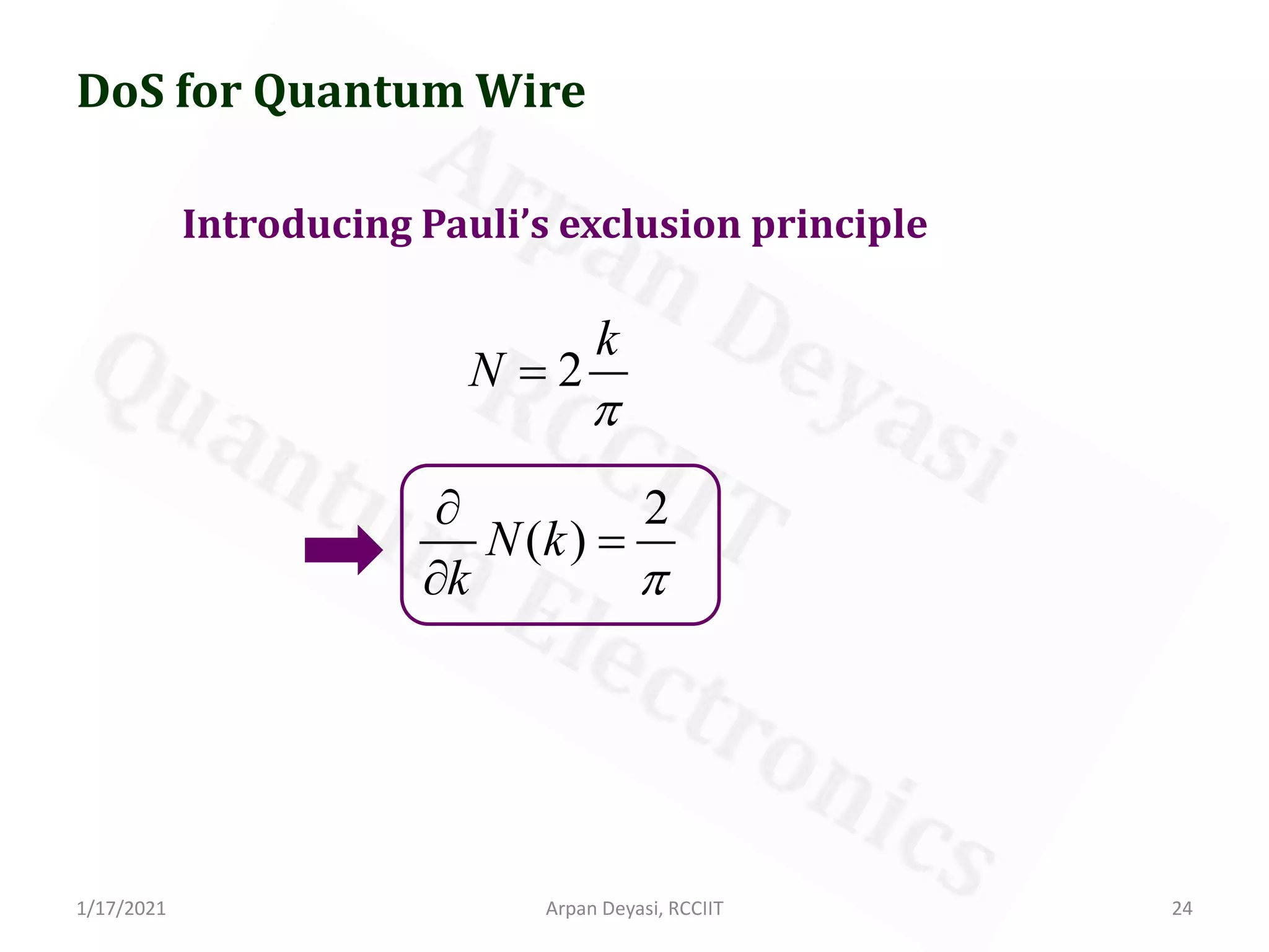
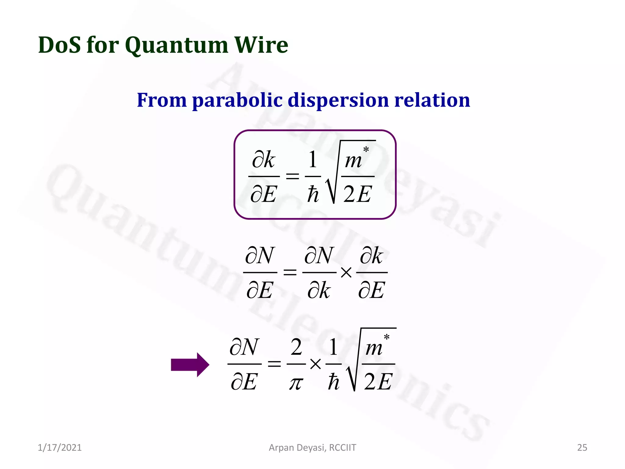
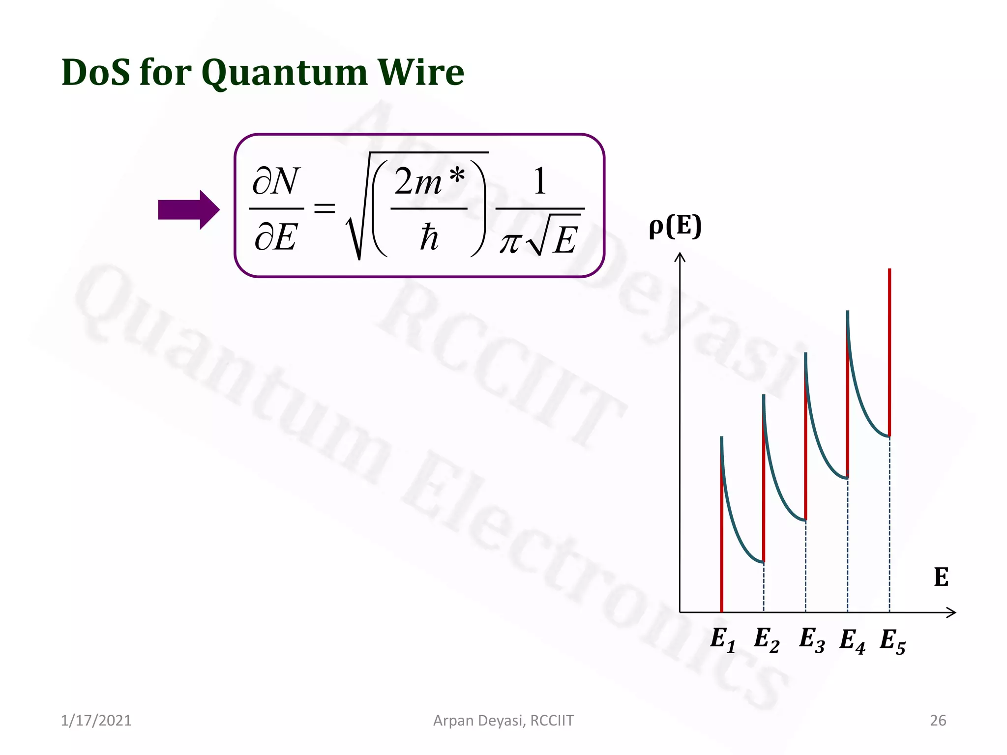
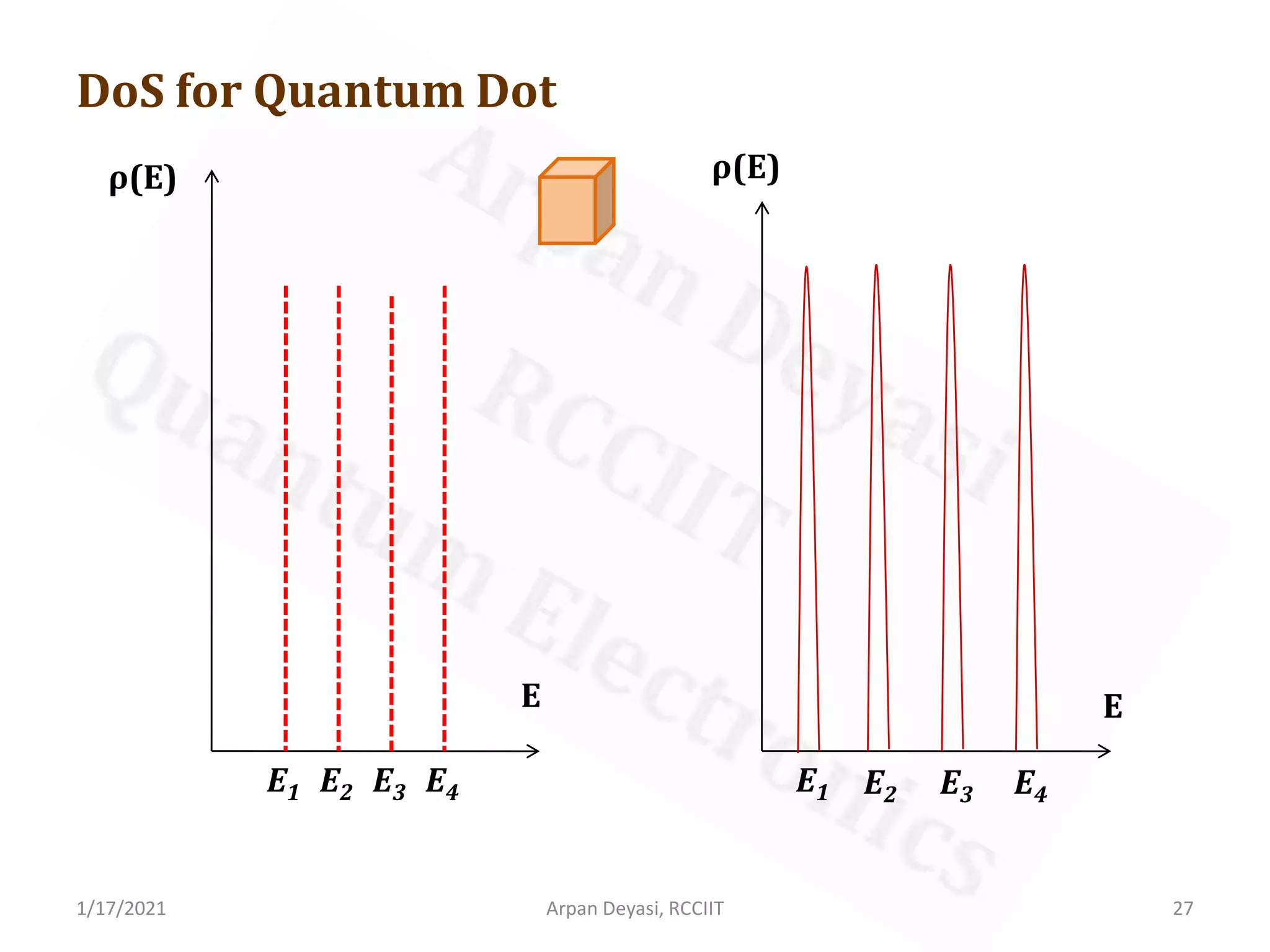
SlideShare a Scribd company logo
Course: Quantum Electronics
Arpan Deyasi
Topic: Density of states of Bulk and Quantum
Structures
1
Arpan Deyasi, RCCIIT
1/17/2021
1/17/2021 2Arpan Deyasi, RCCIIT
What is DoS?
Number of available energy states
per unit energy interval
per unit dimension
in real space
EC
EC + dEC
EV
EV + dEV
dEV
dEC
E
k
1/17/2021 Arpan Deyasi, RCCIIT 3
What do we mean by ‘dimension’?
For ‘bulk’, it is ‘volume’
For ‘quantum well’, it is ‘area/surface’
For ‘quantum wire’, it is ‘line/length’
For ‘quantum dot’, it is a ‘point/dot’
1/17/2021 4Arpan Deyasi, RCCIIT
Energy band diagram is drawn in E-k plane
‘k’ is wave-vector, not a physical quantity
No of electrons is measured by magnitude of current
So we must know the density of electrons
in real space instead of k-space
1/17/2021 Arpan Deyasi, RCCIIT 5
Fermi sphere
1/17/2021 Arpan Deyasi, RCCIIT 6
Fermi surface
1/17/2021 7Arpan Deyasi, RCCIIT
DoS for bulk semiconductor
Let’s start with Bloch theorem
( , , ) ( , , )x y zx y z x L y L z Lψ ψ= + + +
Consider a 3D semiconductor with dimensions Lx, Ly, Lz
1/17/2021 8Arpan Deyasi, RCCIIT
DoS for bulk semiconductor
For validity of wave function
2
2
2
x x x
y y y
z z z
k L n
k L n
k L n
π
π
π
=
=
=
Volume in k-space
3
(2 ) x y z
x y z
x y z
n n n
k k k
L L L
π
=
1/17/2021 9Arpan Deyasi, RCCIIT
DoS for bulk semiconductor
Let
1x y zn n n= = =
x y zL L L L= = =
Volume of unit cell in k-space
3
3
(2 )
kV
L
π
=
1/17/2021 10Arpan Deyasi, RCCIIT
DoS for bulk semiconductor
Volume of Fermi sphere in k-space
34
3
FV kπ=
Volume of semiconductor in real space
3
RV L=
1/17/2021 11Arpan Deyasi, RCCIIT
DoS for bulk semiconductor
number of energy states in real space
1 1
F
k R
N V
V V
= × ×
3
3
3 3
4 1
3 8
L
N k
L
π
π
= × ×
3
2
( )
6
k
N N k
π
= =
1/17/2021 12Arpan Deyasi, RCCIIT
DoS for bulk semiconductor
Introducing Pauli’s exclusion principle
3 3
2 2
( ) 2
6 3
k k
N k
π π
=× =
2
2
( )
k
N k
k π
∂
=
∂
1/17/2021 13Arpan Deyasi, RCCIIT
DoS for bulk semiconductor
From parabolic dispersion relation
2 2
*
2
k
E
m
=

2
*
E k
k m
∂
=
∂

2
* *
2 * 2E m E E
k m m
∂
= =
∂



1/17/2021 14Arpan Deyasi, RCCIIT
DoS for bulk semiconductor
*
1
2
k m
E E
∂
=
∂ 
N N k
E k E
∂ ∂ ∂
= ×
∂ ∂ ∂
2 *
2
1
2
N k m
E Eπ
∂
= ×
∂ 
1/17/2021 15Arpan Deyasi, RCCIIT
DoS for bulk semiconductor
*
2 2
2 * 1
2
N m E m
E Eπ
∂
= ×
∂  
3/2*
2 2
1 2
2
N m
E
E π
 ∂
= × 
∂  
For a particular material
N
E
E
∂
∝
∂
E
ρ(E)
1/17/2021 16Arpan Deyasi, RCCIIT
DoS for Quantum Well
Area in k-space
2
2
(2 )
kA
L
π
=
Area of Fermi sphere in k-space
Area of semiconductor in real space
2
FA kπ=
2
RA L=
1/17/2021 17Arpan Deyasi, RCCIIT
DoS for Quantum Well
number of energy states in real space
1 1
F
k R
N A
A A
= × ×
2
2
2 2
1
4
L
N k
L
π
π
= × ×
2
( )
4
k
N N k
π
= =
1/17/2021 18Arpan Deyasi, RCCIIT
DoS for Quantum Well
Introducing Pauli’s exclusion principle
2 2
( ) 2
4 2
k k
N k
π π
=× =
( )
k
N k
k π
∂
=
∂
1/17/2021 19Arpan Deyasi, RCCIIT
DoS for Quantum Well
From parabolic dispersion relation
*
1
2
k m
E E
∂
=
∂ 
N N k
E k E
∂ ∂ ∂
= ×
∂ ∂ ∂
*
1
2
N k m
E Eπ
∂
= ×
∂ 
1/17/2021 20Arpan Deyasi, RCCIIT
DoS for Quantum Well
* *
2 1
2
N m E m
E Eπ
∂
= ×
∂  
*
2
N m
E π
∂
=
∂ 
DoS is independent of energy?
1/17/2021 21Arpan Deyasi, RCCIIT
DoS for Quantum Well
The result is obtained for a particular sub-band
Considering all the sub-bands
*
2
1
( )
n
i
i
N m
E E
E π =
∂
= Θ −
∂
∑
E
ρ(E)
E1 E2 E3 Ei-1 Ei Ei+1
1/17/2021 22Arpan Deyasi, RCCIIT
DoS for Quantum Wire
Length in k-space
Length of Fermi sphere in k-space
Length of semiconductor in real space
2
kL
L
π
=
2FL k=
RL L=
1/17/2021 23Arpan Deyasi, RCCIIT
DoS for Quantum Wire
number of energy states in real space
1 1
F
k R
N L
L L
= × ×
1
2
2
L
N k
Lπ
= × ×
k
N
π
=
1/17/2021 24Arpan Deyasi, RCCIIT
DoS for Quantum Wire
Introducing Pauli’s exclusion principle
2
k
N
π
=
2
( )N k
k π
∂
=
∂
1/17/2021 25Arpan Deyasi, RCCIIT
DoS for Quantum Wire
From parabolic dispersion relation
*
1
2
k m
E E
∂
=
∂ 
N N k
E k E
∂ ∂ ∂
= ×
∂ ∂ ∂
*
2 1
2
N m
E Eπ
∂
= ×
∂ 
1/17/2021 26Arpan Deyasi, RCCIIT
DoS for Quantum Wire
2 * 1N m
E Eπ
∂  
=  
∂  
E
ρ(E)
E1 E2 E3 E4 E5
1/17/2021 27Arpan Deyasi, RCCIIT
DoS for Quantum Dot
E4E3E2E1
ρ(E)
E E
ρ(E)
E1 E2 E3 E4

More Related Content

What's hot

Foundation of Optoelectronics
Foundation of OptoelectronicsFoundation of Optoelectronics
Foundation of Optoelectronics
RCC Institute of Information Technology
 
Fermi Level
Fermi LevelFermi Level
Metal-Semiconductor Contact
Metal-Semiconductor ContactMetal-Semiconductor Contact
Metal-Semiconductor Contact
RCC Institute of Information Technology
 
Optoelectronics seminar: MESFET
Optoelectronics seminar: MESFETOptoelectronics seminar: MESFET
Optoelectronics seminar: MESFET
Mridula Sharma
 
Various configurations in BJT
Various configurations in BJTVarious configurations in BJT
Various configurations in BJT
RCC Institute of Information Technology
 
Electrical characteristics of MOSFET
Electrical characteristics of MOSFETElectrical characteristics of MOSFET
Electrical characteristics of MOSFET
RCC Institute of Information Technology
 
Short-Channel Effects in MOSFET
Short-Channel Effects in MOSFETShort-Channel Effects in MOSFET
Short-Channel Effects in MOSFET
RCC Institute of Information Technology
 
Density of states of bulk semiconductor
Density of states of bulk semiconductorDensity of states of bulk semiconductor
Density of states of bulk semiconductor
RCC Institute of Information Technology
 
MESFET
MESFETMESFET
Optoelectronics
OptoelectronicsOptoelectronics
Optoelectronics
DEPARTMENT OF PHYSICS
 
Foundation of optical transmitter
Foundation of optical transmitterFoundation of optical transmitter
Foundation of optical transmitter
RCC Institute of Information Technology
 
Tunnel diode
Tunnel diodeTunnel diode
Chapter 4b
Chapter 4bChapter 4b
Chapter 4b
Gabriel O'Brien
 
Hall Effect
Hall EffectHall Effect
Metal semiconductor contacts
Metal semiconductor contactsMetal semiconductor contacts
Metal semiconductor contacts
Kasif Nabi
 
Ece 334 lecture 15-mosfet-basics
Ece 334 lecture 15-mosfet-basicsEce 334 lecture 15-mosfet-basics
Ece 334 lecture 15-mosfet-basics
Muhammad Naveed Sultan
 
Q-V characteristics of MOS Capacitor
Q-V characteristics of MOS CapacitorQ-V characteristics of MOS Capacitor
Q-V characteristics of MOS Capacitor
RCC Institute of Information Technology
 
Built-in potential and extrinsic Fermi level in p-n junction diode
Built-in potential and extrinsic Fermi level in p-n junction diodeBuilt-in potential and extrinsic Fermi level in p-n junction diode
Built-in potential and extrinsic Fermi level in p-n junction diode
RCC Institute of Information Technology
 
JFET
JFETJFET
Semiconductor optoelectronic materials
Semiconductor optoelectronic materialsSemiconductor optoelectronic materials
Semiconductor optoelectronic materials
krishslide
 

What's hot (20)

Foundation of Optoelectronics
Foundation of OptoelectronicsFoundation of Optoelectronics
Foundation of Optoelectronics
 
Fermi Level
Fermi LevelFermi Level
Fermi Level
 
Metal-Semiconductor Contact
Metal-Semiconductor ContactMetal-Semiconductor Contact
Metal-Semiconductor Contact
 
Optoelectronics seminar: MESFET
Optoelectronics seminar: MESFETOptoelectronics seminar: MESFET
Optoelectronics seminar: MESFET
 
Various configurations in BJT
Various configurations in BJTVarious configurations in BJT
Various configurations in BJT
 
Electrical characteristics of MOSFET
Electrical characteristics of MOSFETElectrical characteristics of MOSFET
Electrical characteristics of MOSFET
 
Short-Channel Effects in MOSFET
Short-Channel Effects in MOSFETShort-Channel Effects in MOSFET
Short-Channel Effects in MOSFET
 
Density of states of bulk semiconductor
Density of states of bulk semiconductorDensity of states of bulk semiconductor
Density of states of bulk semiconductor
 
MESFET
MESFETMESFET
MESFET
 
Optoelectronics
OptoelectronicsOptoelectronics
Optoelectronics
 
Foundation of optical transmitter
Foundation of optical transmitterFoundation of optical transmitter
Foundation of optical transmitter
 
Tunnel diode
Tunnel diodeTunnel diode
Tunnel diode
 
Chapter 4b
Chapter 4bChapter 4b
Chapter 4b
 
Hall Effect
Hall EffectHall Effect
Hall Effect
 
Metal semiconductor contacts
Metal semiconductor contactsMetal semiconductor contacts
Metal semiconductor contacts
 
Ece 334 lecture 15-mosfet-basics
Ece 334 lecture 15-mosfet-basicsEce 334 lecture 15-mosfet-basics
Ece 334 lecture 15-mosfet-basics
 
Q-V characteristics of MOS Capacitor
Q-V characteristics of MOS CapacitorQ-V characteristics of MOS Capacitor
Q-V characteristics of MOS Capacitor
 
Built-in potential and extrinsic Fermi level in p-n junction diode
Built-in potential and extrinsic Fermi level in p-n junction diodeBuilt-in potential and extrinsic Fermi level in p-n junction diode
Built-in potential and extrinsic Fermi level in p-n junction diode
 
JFET
JFETJFET
JFET
 
Semiconductor optoelectronic materials
Semiconductor optoelectronic materialsSemiconductor optoelectronic materials
Semiconductor optoelectronic materials
 

Similar to DoS of bulk and quantum structures

Absorption coefficient of quantum well structure
Absorption coefficient of quantum well structure Absorption coefficient of quantum well structure
Absorption coefficient of quantum well structure
RCC Institute of Information Technology
 
absorption coefficient in bulk and quantum well structure
absorption coefficient in bulk and quantum well structureabsorption coefficient in bulk and quantum well structure
absorption coefficient in bulk and quantum well structure
RCC Institute of Information Technology
 
Band nonparabolicity effect on eigenstates
Band nonparabolicity effect on eigenstatesBand nonparabolicity effect on eigenstates
Band nonparabolicity effect on eigenstates
RCC Institute of Information Technology
 
Capacitor
CapacitorCapacitor
King_Notes_Density_of_States_2D1D0D.pdf
King_Notes_Density_of_States_2D1D0D.pdfKing_Notes_Density_of_States_2D1D0D.pdf
King_Notes_Density_of_States_2D1D0D.pdf
LogeshwariC2
 
Telegrapher's Equation
Telegrapher's EquationTelegrapher's Equation
Fundamentals of Gauss' Law
Fundamentals of Gauss' LawFundamentals of Gauss' Law
Fundamentals of Gauss' Law
RCC Institute of Information Technology
 
Semiconductor laser
Semiconductor laserSemiconductor laser
ELECTRODYNAMIC FIELDS
ELECTRODYNAMIC FIELDSELECTRODYNAMIC FIELDS
ELECTRODYNAMIC FIELDS
Karthik Kathan
 
Carrier transport processes
Carrier transport processesCarrier transport processes
Carrier transport processes
RCC Institute of Information Technology
 
Application of Gauss' Law
Application of Gauss' LawApplication of Gauss' Law
Application of Gauss' Law
RCC Institute of Information Technology
 
Ch1 slides-1
Ch1 slides-1Ch1 slides-1
Ch1 slides-1
CahyaniWindarto2
 
G24041050
G24041050G24041050
G24041050
IJERA Editor
 
Distortionless Transmission Line
Distortionless Transmission LineDistortionless Transmission Line
Distortionless Transmission Line
RCC Institute of Information Technology
 
Semiconductor nanodevices
Semiconductor nanodevicesSemiconductor nanodevices
Semiconductor nanodevices
Atif Syed
 
Fundamentals of Coulomb's Law
Fundamentals of Coulomb's LawFundamentals of Coulomb's Law
Fundamentals of Coulomb's Law
RCC Institute of Information Technology
 
Gain parameters of BJT
Gain parameters of BJTGain parameters of BJT
Electrical properties of p-n junction
Electrical properties of p-n junctionElectrical properties of p-n junction
Electrical properties of p-n junction
RCC Institute of Information Technology
 
Quantum Electronics Lecture 7
Quantum Electronics Lecture 7Quantum Electronics Lecture 7
Quantum Electronics Lecture 7
RCC Institute of Information Technology
 
Effective mass
Effective massEffective mass

Similar to DoS of bulk and quantum structures (20)

Absorption coefficient of quantum well structure
Absorption coefficient of quantum well structure Absorption coefficient of quantum well structure
Absorption coefficient of quantum well structure
 
absorption coefficient in bulk and quantum well structure
absorption coefficient in bulk and quantum well structureabsorption coefficient in bulk and quantum well structure
absorption coefficient in bulk and quantum well structure
 
Band nonparabolicity effect on eigenstates
Band nonparabolicity effect on eigenstatesBand nonparabolicity effect on eigenstates
Band nonparabolicity effect on eigenstates
 
Capacitor
CapacitorCapacitor
Capacitor
 
King_Notes_Density_of_States_2D1D0D.pdf
King_Notes_Density_of_States_2D1D0D.pdfKing_Notes_Density_of_States_2D1D0D.pdf
King_Notes_Density_of_States_2D1D0D.pdf
 
Telegrapher's Equation
Telegrapher's EquationTelegrapher's Equation
Telegrapher's Equation
 
Fundamentals of Gauss' Law
Fundamentals of Gauss' LawFundamentals of Gauss' Law
Fundamentals of Gauss' Law
 
Semiconductor laser
Semiconductor laserSemiconductor laser
Semiconductor laser
 
ELECTRODYNAMIC FIELDS
ELECTRODYNAMIC FIELDSELECTRODYNAMIC FIELDS
ELECTRODYNAMIC FIELDS
 
Carrier transport processes
Carrier transport processesCarrier transport processes
Carrier transport processes
 
Application of Gauss' Law
Application of Gauss' LawApplication of Gauss' Law
Application of Gauss' Law
 
Ch1 slides-1
Ch1 slides-1Ch1 slides-1
Ch1 slides-1
 
G24041050
G24041050G24041050
G24041050
 
Distortionless Transmission Line
Distortionless Transmission LineDistortionless Transmission Line
Distortionless Transmission Line
 
Semiconductor nanodevices
Semiconductor nanodevicesSemiconductor nanodevices
Semiconductor nanodevices
 
Fundamentals of Coulomb's Law
Fundamentals of Coulomb's LawFundamentals of Coulomb's Law
Fundamentals of Coulomb's Law
 
Gain parameters of BJT
Gain parameters of BJTGain parameters of BJT
Gain parameters of BJT
 
Electrical properties of p-n junction
Electrical properties of p-n junctionElectrical properties of p-n junction
Electrical properties of p-n junction
 
Quantum Electronics Lecture 7
Quantum Electronics Lecture 7Quantum Electronics Lecture 7
Quantum Electronics Lecture 7
 
Effective mass
Effective massEffective mass
Effective mass
 

More from RCC Institute of Information Technology

Scaling in conventional MOSFET for constant electric field and constant voltage
Scaling in conventional MOSFET for constant electric field and constant voltageScaling in conventional MOSFET for constant electric field and constant voltage
Scaling in conventional MOSFET for constant electric field and constant voltage
RCC Institute of Information Technology
 
Carrier scattering and ballistic transport
Carrier scattering and ballistic transportCarrier scattering and ballistic transport
Carrier scattering and ballistic transport
RCC Institute of Information Technology
 
Electromagnetic Wave Propagations
Electromagnetic Wave PropagationsElectromagnetic Wave Propagations
Electromagnetic Wave Propagations
RCC Institute of Information Technology
 
Biot-Savart law
Biot-Savart lawBiot-Savart law
Ampere's circuital law
Ampere's circuital lawAmpere's circuital law
Magnetic Potentials
Magnetic PotentialsMagnetic Potentials
Reflection and Transmission coefficients in transmission line
Reflection and Transmission coefficients in transmission lineReflection and Transmission coefficients in transmission line
Reflection and Transmission coefficients in transmission line
RCC Institute of Information Technology
 
Impedance in transmission line
Impedance in transmission lineImpedance in transmission line
Impedance in transmission line
RCC Institute of Information Technology
 
Quantum Hall Effect
Quantum Hall EffectQuantum Hall Effect
Dielectrics
DielectricsDielectrics
Electrical Properties of Dipole
Electrical Properties of DipoleElectrical Properties of Dipole
Electrical Properties of Dipole
RCC Institute of Information Technology
 
Vector Integration
Vector IntegrationVector Integration
Scalar and vector differentiation
Scalar and vector differentiationScalar and vector differentiation
Scalar and vector differentiation
RCC Institute of Information Technology
 
Coordinate transformation
Coordinate transformationCoordinate transformation
Coordinate transformation
RCC Institute of Information Technology
 
Moletronics
MoletronicsMoletronics
Crystal Growth
Crystal GrowthCrystal Growth
Memristor
MemristorMemristor
Advanced MOSFET
Advanced MOSFETAdvanced MOSFET
CNTFET
CNTFETCNTFET
High Electron Mobility Transistor
High Electron Mobility TransistorHigh Electron Mobility Transistor
High Electron Mobility Transistor
RCC Institute of Information Technology
 

More from RCC Institute of Information Technology (20)

Scaling in conventional MOSFET for constant electric field and constant voltage
Scaling in conventional MOSFET for constant electric field and constant voltageScaling in conventional MOSFET for constant electric field and constant voltage
Scaling in conventional MOSFET for constant electric field and constant voltage
 
Carrier scattering and ballistic transport
Carrier scattering and ballistic transportCarrier scattering and ballistic transport
Carrier scattering and ballistic transport
 
Electromagnetic Wave Propagations
Electromagnetic Wave PropagationsElectromagnetic Wave Propagations
Electromagnetic Wave Propagations
 
Biot-Savart law
Biot-Savart lawBiot-Savart law
Biot-Savart law
 
Ampere's circuital law
Ampere's circuital lawAmpere's circuital law
Ampere's circuital law
 
Magnetic Potentials
Magnetic PotentialsMagnetic Potentials
Magnetic Potentials
 
Reflection and Transmission coefficients in transmission line
Reflection and Transmission coefficients in transmission lineReflection and Transmission coefficients in transmission line
Reflection and Transmission coefficients in transmission line
 
Impedance in transmission line
Impedance in transmission lineImpedance in transmission line
Impedance in transmission line
 
Quantum Hall Effect
Quantum Hall EffectQuantum Hall Effect
Quantum Hall Effect
 
Dielectrics
DielectricsDielectrics
Dielectrics
 
Electrical Properties of Dipole
Electrical Properties of DipoleElectrical Properties of Dipole
Electrical Properties of Dipole
 
Vector Integration
Vector IntegrationVector Integration
Vector Integration
 
Scalar and vector differentiation
Scalar and vector differentiationScalar and vector differentiation
Scalar and vector differentiation
 
Coordinate transformation
Coordinate transformationCoordinate transformation
Coordinate transformation
 
Moletronics
MoletronicsMoletronics
Moletronics
 
Crystal Growth
Crystal GrowthCrystal Growth
Crystal Growth
 
Memristor
MemristorMemristor
Memristor
 
Advanced MOSFET
Advanced MOSFETAdvanced MOSFET
Advanced MOSFET
 
CNTFET
CNTFETCNTFET
CNTFET
 
High Electron Mobility Transistor
High Electron Mobility TransistorHigh Electron Mobility Transistor
High Electron Mobility Transistor
 

Recently uploaded

AN INTRODUCTION OF AI & SEARCHING TECHIQUES
AN INTRODUCTION OF AI & SEARCHING TECHIQUESAN INTRODUCTION OF AI & SEARCHING TECHIQUES
AN INTRODUCTION OF AI & SEARCHING TECHIQUES
drshikhapandey2022
 
OOPS_Lab_Manual - programs using C++ programming language
OOPS_Lab_Manual - programs using C++ programming languageOOPS_Lab_Manual - programs using C++ programming language
OOPS_Lab_Manual - programs using C++ programming language
PreethaV16
 
Call For Paper -3rd International Conference on Artificial Intelligence Advan...
Call For Paper -3rd International Conference on Artificial Intelligence Advan...Call For Paper -3rd International Conference on Artificial Intelligence Advan...
Call For Paper -3rd International Conference on Artificial Intelligence Advan...
ijseajournal
 
Determination of Equivalent Circuit parameters and performance characteristic...
Determination of Equivalent Circuit parameters and performance characteristic...Determination of Equivalent Circuit parameters and performance characteristic...
Determination of Equivalent Circuit parameters and performance characteristic...
pvpriya2
 
Beckhoff Programmable Logic Control Overview Presentation
Beckhoff Programmable Logic Control Overview PresentationBeckhoff Programmable Logic Control Overview Presentation
Beckhoff Programmable Logic Control Overview Presentation
VanTuDuong1
 
Levelised Cost of Hydrogen (LCOH) Calculator Manual
Levelised Cost of Hydrogen  (LCOH) Calculator ManualLevelised Cost of Hydrogen  (LCOH) Calculator Manual
Levelised Cost of Hydrogen (LCOH) Calculator Manual
Massimo Talia
 
Supermarket Management System Project Report.pdf
Supermarket Management System Project Report.pdfSupermarket Management System Project Report.pdf
Supermarket Management System Project Report.pdf
Kamal Acharya
 
Sri Guru Hargobind Ji - Bandi Chor Guru.pdf
Sri Guru Hargobind Ji - Bandi Chor Guru.pdfSri Guru Hargobind Ji - Bandi Chor Guru.pdf
Sri Guru Hargobind Ji - Bandi Chor Guru.pdf
Balvir Singh
 
一比一原版(爱大毕业证书)爱荷华大学毕业证如何办理
一比一原版(爱大毕业证书)爱荷华大学毕业证如何办理一比一原版(爱大毕业证书)爱荷华大学毕业证如何办理
一比一原版(爱大毕业证书)爱荷华大学毕业证如何办理
nedcocy
 
SENTIMENT ANALYSIS ON PPT AND Project template_.pptx
SENTIMENT ANALYSIS ON PPT AND Project template_.pptxSENTIMENT ANALYSIS ON PPT AND Project template_.pptx
SENTIMENT ANALYSIS ON PPT AND Project template_.pptx
b0754201
 
Null Bangalore | Pentesters Approach to AWS IAM
Null Bangalore | Pentesters Approach to AWS IAMNull Bangalore | Pentesters Approach to AWS IAM
Null Bangalore | Pentesters Approach to AWS IAM
Divyanshu
 
SELENIUM CONF -PALLAVI SHARMA - 2024.pdf
SELENIUM CONF -PALLAVI SHARMA - 2024.pdfSELENIUM CONF -PALLAVI SHARMA - 2024.pdf
SELENIUM CONF -PALLAVI SHARMA - 2024.pdf
Pallavi Sharma
 
Tools & Techniques for Commissioning and Maintaining PV Systems W-Animations ...
Tools & Techniques for Commissioning and Maintaining PV Systems W-Animations ...Tools & Techniques for Commissioning and Maintaining PV Systems W-Animations ...
Tools & Techniques for Commissioning and Maintaining PV Systems W-Animations ...
Transcat
 
AI + Data Community Tour - Build the Next Generation of Apps with the Einstei...
AI + Data Community Tour - Build the Next Generation of Apps with the Einstei...AI + Data Community Tour - Build the Next Generation of Apps with the Einstei...
AI + Data Community Tour - Build the Next Generation of Apps with the Einstei...
Paris Salesforce Developer Group
 
Height and depth gauge linear metrology.pdf
Height and depth gauge linear metrology.pdfHeight and depth gauge linear metrology.pdf
Height and depth gauge linear metrology.pdf
q30122000
 
Call Girls Chennai +91-8824825030 Vip Call Girls Chennai
Call Girls Chennai +91-8824825030 Vip Call Girls ChennaiCall Girls Chennai +91-8824825030 Vip Call Girls Chennai
Call Girls Chennai +91-8824825030 Vip Call Girls Chennai
paraasingh12 #V08
 
EV BMS WITH CHARGE MONITOR AND FIRE DETECTION.pptx
EV BMS WITH CHARGE MONITOR AND FIRE DETECTION.pptxEV BMS WITH CHARGE MONITOR AND FIRE DETECTION.pptx
EV BMS WITH CHARGE MONITOR AND FIRE DETECTION.pptx
nikshimanasa
 
Digital Twins Computer Networking Paper Presentation.pptx
Digital Twins Computer Networking Paper Presentation.pptxDigital Twins Computer Networking Paper Presentation.pptx
Digital Twins Computer Networking Paper Presentation.pptx
aryanpankaj78
 
openshift technical overview - Flow of openshift containerisatoin
openshift technical overview - Flow of openshift containerisatoinopenshift technical overview - Flow of openshift containerisatoin
openshift technical overview - Flow of openshift containerisatoin
snaprevwdev
 
Object Oriented Analysis and Design - OOAD
Object Oriented Analysis and Design - OOADObject Oriented Analysis and Design - OOAD
Object Oriented Analysis and Design - OOAD
PreethaV16
 

Recently uploaded (20)

AN INTRODUCTION OF AI & SEARCHING TECHIQUES
AN INTRODUCTION OF AI & SEARCHING TECHIQUESAN INTRODUCTION OF AI & SEARCHING TECHIQUES
AN INTRODUCTION OF AI & SEARCHING TECHIQUES
 
OOPS_Lab_Manual - programs using C++ programming language
OOPS_Lab_Manual - programs using C++ programming languageOOPS_Lab_Manual - programs using C++ programming language
OOPS_Lab_Manual - programs using C++ programming language
 
Call For Paper -3rd International Conference on Artificial Intelligence Advan...
Call For Paper -3rd International Conference on Artificial Intelligence Advan...Call For Paper -3rd International Conference on Artificial Intelligence Advan...
Call For Paper -3rd International Conference on Artificial Intelligence Advan...
 
Determination of Equivalent Circuit parameters and performance characteristic...
Determination of Equivalent Circuit parameters and performance characteristic...Determination of Equivalent Circuit parameters and performance characteristic...
Determination of Equivalent Circuit parameters and performance characteristic...
 
Beckhoff Programmable Logic Control Overview Presentation
Beckhoff Programmable Logic Control Overview PresentationBeckhoff Programmable Logic Control Overview Presentation
Beckhoff Programmable Logic Control Overview Presentation
 
Levelised Cost of Hydrogen (LCOH) Calculator Manual
Levelised Cost of Hydrogen  (LCOH) Calculator ManualLevelised Cost of Hydrogen  (LCOH) Calculator Manual
Levelised Cost of Hydrogen (LCOH) Calculator Manual
 
Supermarket Management System Project Report.pdf
Supermarket Management System Project Report.pdfSupermarket Management System Project Report.pdf
Supermarket Management System Project Report.pdf
 
Sri Guru Hargobind Ji - Bandi Chor Guru.pdf
Sri Guru Hargobind Ji - Bandi Chor Guru.pdfSri Guru Hargobind Ji - Bandi Chor Guru.pdf
Sri Guru Hargobind Ji - Bandi Chor Guru.pdf
 
一比一原版(爱大毕业证书)爱荷华大学毕业证如何办理
一比一原版(爱大毕业证书)爱荷华大学毕业证如何办理一比一原版(爱大毕业证书)爱荷华大学毕业证如何办理
一比一原版(爱大毕业证书)爱荷华大学毕业证如何办理
 
SENTIMENT ANALYSIS ON PPT AND Project template_.pptx
SENTIMENT ANALYSIS ON PPT AND Project template_.pptxSENTIMENT ANALYSIS ON PPT AND Project template_.pptx
SENTIMENT ANALYSIS ON PPT AND Project template_.pptx
 
Null Bangalore | Pentesters Approach to AWS IAM
Null Bangalore | Pentesters Approach to AWS IAMNull Bangalore | Pentesters Approach to AWS IAM
Null Bangalore | Pentesters Approach to AWS IAM
 
SELENIUM CONF -PALLAVI SHARMA - 2024.pdf
SELENIUM CONF -PALLAVI SHARMA - 2024.pdfSELENIUM CONF -PALLAVI SHARMA - 2024.pdf
SELENIUM CONF -PALLAVI SHARMA - 2024.pdf
 
Tools & Techniques for Commissioning and Maintaining PV Systems W-Animations ...
Tools & Techniques for Commissioning and Maintaining PV Systems W-Animations ...Tools & Techniques for Commissioning and Maintaining PV Systems W-Animations ...
Tools & Techniques for Commissioning and Maintaining PV Systems W-Animations ...
 
AI + Data Community Tour - Build the Next Generation of Apps with the Einstei...
AI + Data Community Tour - Build the Next Generation of Apps with the Einstei...AI + Data Community Tour - Build the Next Generation of Apps with the Einstei...
AI + Data Community Tour - Build the Next Generation of Apps with the Einstei...
 
Height and depth gauge linear metrology.pdf
Height and depth gauge linear metrology.pdfHeight and depth gauge linear metrology.pdf
Height and depth gauge linear metrology.pdf
 
Call Girls Chennai +91-8824825030 Vip Call Girls Chennai
Call Girls Chennai +91-8824825030 Vip Call Girls ChennaiCall Girls Chennai +91-8824825030 Vip Call Girls Chennai
Call Girls Chennai +91-8824825030 Vip Call Girls Chennai
 
EV BMS WITH CHARGE MONITOR AND FIRE DETECTION.pptx
EV BMS WITH CHARGE MONITOR AND FIRE DETECTION.pptxEV BMS WITH CHARGE MONITOR AND FIRE DETECTION.pptx
EV BMS WITH CHARGE MONITOR AND FIRE DETECTION.pptx
 
Digital Twins Computer Networking Paper Presentation.pptx
Digital Twins Computer Networking Paper Presentation.pptxDigital Twins Computer Networking Paper Presentation.pptx
Digital Twins Computer Networking Paper Presentation.pptx
 
openshift technical overview - Flow of openshift containerisatoin
openshift technical overview - Flow of openshift containerisatoinopenshift technical overview - Flow of openshift containerisatoin
openshift technical overview - Flow of openshift containerisatoin
 
Object Oriented Analysis and Design - OOAD
Object Oriented Analysis and Design - OOADObject Oriented Analysis and Design - OOAD
Object Oriented Analysis and Design - OOAD
 

DoS of bulk and quantum structures

  • 1. Course: Quantum Electronics Arpan Deyasi Topic: Density of states of Bulk and Quantum Structures 1 Arpan Deyasi, RCCIIT 1/17/2021
  • 2. 1/17/2021 2Arpan Deyasi, RCCIIT What is DoS? Number of available energy states per unit energy interval per unit dimension in real space EC EC + dEC EV EV + dEV dEV dEC E k
  • 3. 1/17/2021 Arpan Deyasi, RCCIIT 3 What do we mean by ‘dimension’? For ‘bulk’, it is ‘volume’ For ‘quantum well’, it is ‘area/surface’ For ‘quantum wire’, it is ‘line/length’ For ‘quantum dot’, it is a ‘point/dot’
  • 4. 1/17/2021 4Arpan Deyasi, RCCIIT Energy band diagram is drawn in E-k plane ‘k’ is wave-vector, not a physical quantity No of electrons is measured by magnitude of current So we must know the density of electrons in real space instead of k-space
  • 5. 1/17/2021 Arpan Deyasi, RCCIIT 5 Fermi sphere
  • 6. 1/17/2021 Arpan Deyasi, RCCIIT 6 Fermi surface
  • 7. 1/17/2021 7Arpan Deyasi, RCCIIT DoS for bulk semiconductor Let’s start with Bloch theorem ( , , ) ( , , )x y zx y z x L y L z Lψ ψ= + + + Consider a 3D semiconductor with dimensions Lx, Ly, Lz
  • 8. 1/17/2021 8Arpan Deyasi, RCCIIT DoS for bulk semiconductor For validity of wave function 2 2 2 x x x y y y z z z k L n k L n k L n π π π = = = Volume in k-space 3 (2 ) x y z x y z x y z n n n k k k L L L π =
  • 9. 1/17/2021 9Arpan Deyasi, RCCIIT DoS for bulk semiconductor Let 1x y zn n n= = = x y zL L L L= = = Volume of unit cell in k-space 3 3 (2 ) kV L π =
  • 10. 1/17/2021 10Arpan Deyasi, RCCIIT DoS for bulk semiconductor Volume of Fermi sphere in k-space 34 3 FV kπ= Volume of semiconductor in real space 3 RV L=
  • 11. 1/17/2021 11Arpan Deyasi, RCCIIT DoS for bulk semiconductor number of energy states in real space 1 1 F k R N V V V = × × 3 3 3 3 4 1 3 8 L N k L π π = × × 3 2 ( ) 6 k N N k π = =
  • 12. 1/17/2021 12Arpan Deyasi, RCCIIT DoS for bulk semiconductor Introducing Pauli’s exclusion principle 3 3 2 2 ( ) 2 6 3 k k N k π π =× = 2 2 ( ) k N k k π ∂ = ∂
  • 13. 1/17/2021 13Arpan Deyasi, RCCIIT DoS for bulk semiconductor From parabolic dispersion relation 2 2 * 2 k E m =  2 * E k k m ∂ = ∂  2 * * 2 * 2E m E E k m m ∂ = = ∂   
  • 14. 1/17/2021 14Arpan Deyasi, RCCIIT DoS for bulk semiconductor * 1 2 k m E E ∂ = ∂  N N k E k E ∂ ∂ ∂ = × ∂ ∂ ∂ 2 * 2 1 2 N k m E Eπ ∂ = × ∂ 
  • 15. 1/17/2021 15Arpan Deyasi, RCCIIT DoS for bulk semiconductor * 2 2 2 * 1 2 N m E m E Eπ ∂ = × ∂   3/2* 2 2 1 2 2 N m E E π  ∂ = ×  ∂   For a particular material N E E ∂ ∝ ∂ E ρ(E)
  • 16. 1/17/2021 16Arpan Deyasi, RCCIIT DoS for Quantum Well Area in k-space 2 2 (2 ) kA L π = Area of Fermi sphere in k-space Area of semiconductor in real space 2 FA kπ= 2 RA L=
  • 17. 1/17/2021 17Arpan Deyasi, RCCIIT DoS for Quantum Well number of energy states in real space 1 1 F k R N A A A = × × 2 2 2 2 1 4 L N k L π π = × × 2 ( ) 4 k N N k π = =
  • 18. 1/17/2021 18Arpan Deyasi, RCCIIT DoS for Quantum Well Introducing Pauli’s exclusion principle 2 2 ( ) 2 4 2 k k N k π π =× = ( ) k N k k π ∂ = ∂
  • 19. 1/17/2021 19Arpan Deyasi, RCCIIT DoS for Quantum Well From parabolic dispersion relation * 1 2 k m E E ∂ = ∂  N N k E k E ∂ ∂ ∂ = × ∂ ∂ ∂ * 1 2 N k m E Eπ ∂ = × ∂ 
  • 20. 1/17/2021 20Arpan Deyasi, RCCIIT DoS for Quantum Well * * 2 1 2 N m E m E Eπ ∂ = × ∂   * 2 N m E π ∂ = ∂  DoS is independent of energy?
  • 21. 1/17/2021 21Arpan Deyasi, RCCIIT DoS for Quantum Well The result is obtained for a particular sub-band Considering all the sub-bands * 2 1 ( ) n i i N m E E E π = ∂ = Θ − ∂ ∑ E ρ(E) E1 E2 E3 Ei-1 Ei Ei+1
  • 22. 1/17/2021 22Arpan Deyasi, RCCIIT DoS for Quantum Wire Length in k-space Length of Fermi sphere in k-space Length of semiconductor in real space 2 kL L π = 2FL k= RL L=
  • 23. 1/17/2021 23Arpan Deyasi, RCCIIT DoS for Quantum Wire number of energy states in real space 1 1 F k R N L L L = × × 1 2 2 L N k Lπ = × × k N π =
  • 24. 1/17/2021 24Arpan Deyasi, RCCIIT DoS for Quantum Wire Introducing Pauli’s exclusion principle 2 k N π = 2 ( )N k k π ∂ = ∂
  • 25. 1/17/2021 25Arpan Deyasi, RCCIIT DoS for Quantum Wire From parabolic dispersion relation * 1 2 k m E E ∂ = ∂  N N k E k E ∂ ∂ ∂ = × ∂ ∂ ∂ * 2 1 2 N m E Eπ ∂ = × ∂ 
  • 26. 1/17/2021 26Arpan Deyasi, RCCIIT DoS for Quantum Wire 2 * 1N m E Eπ ∂   =   ∂   E ρ(E) E1 E2 E3 E4 E5
  • 27. 1/17/2021 27Arpan Deyasi, RCCIIT DoS for Quantum Dot E4E3E2E1 ρ(E) E E ρ(E) E1 E2 E3 E4