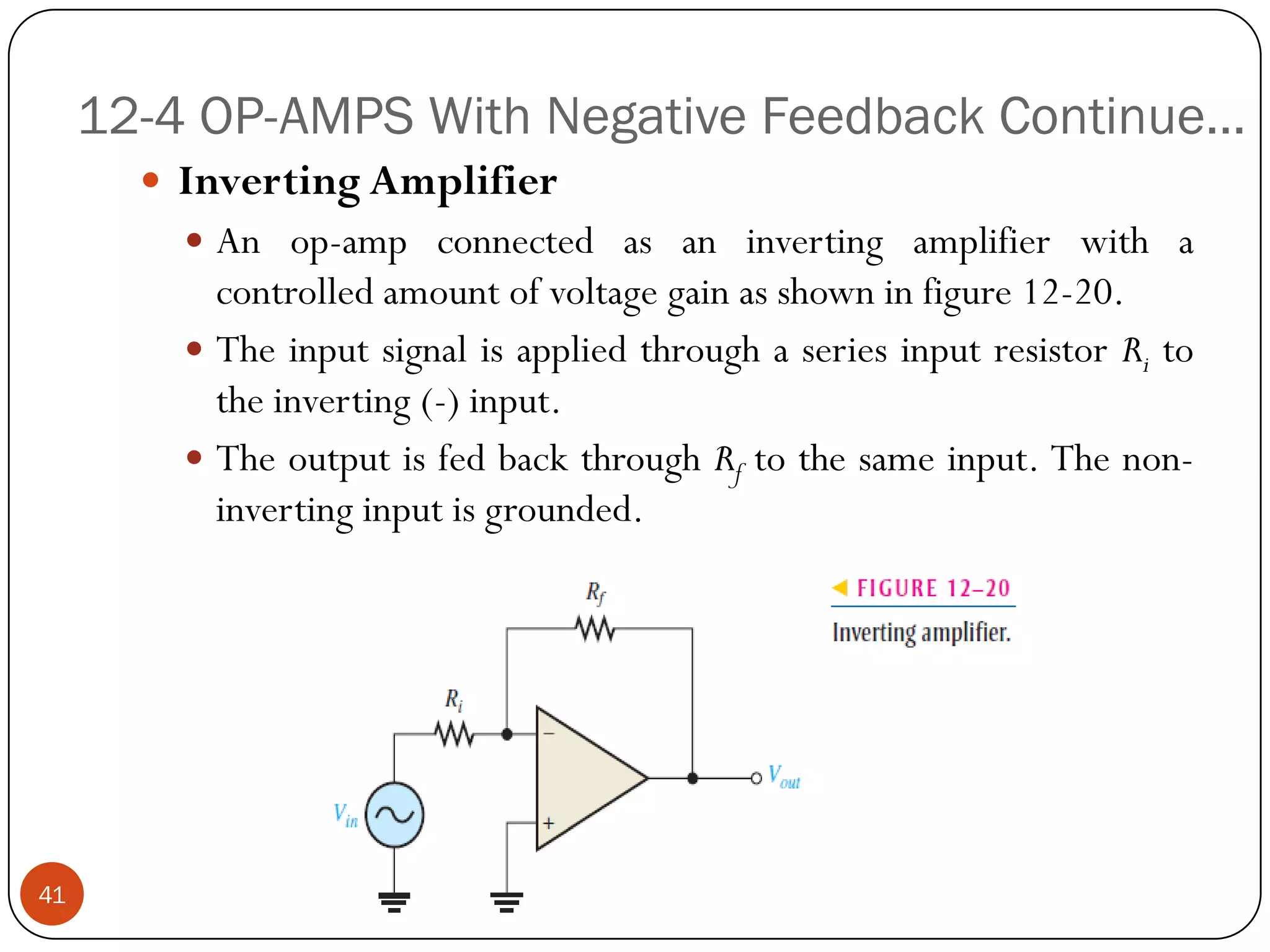
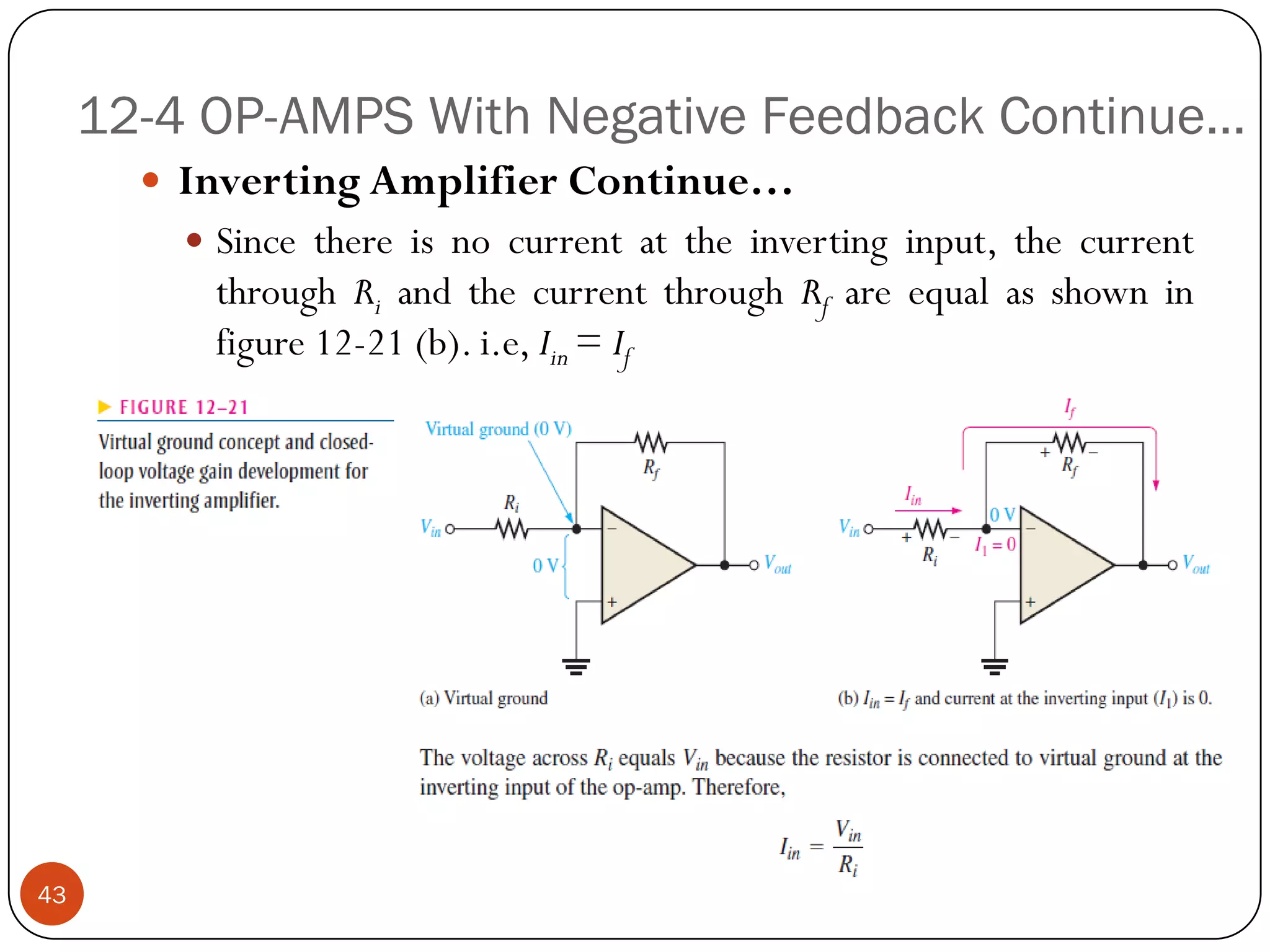
Download as PDF, PPTX
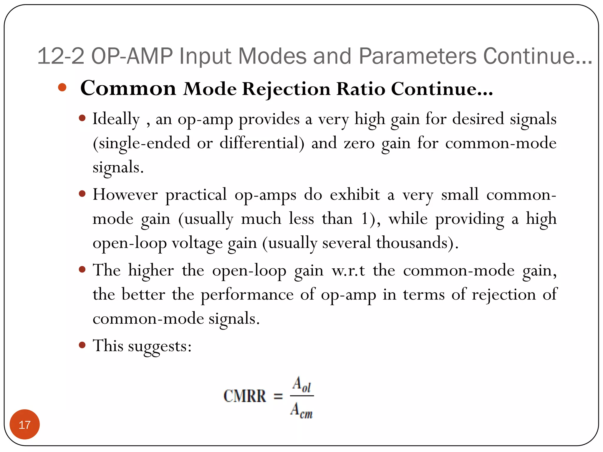
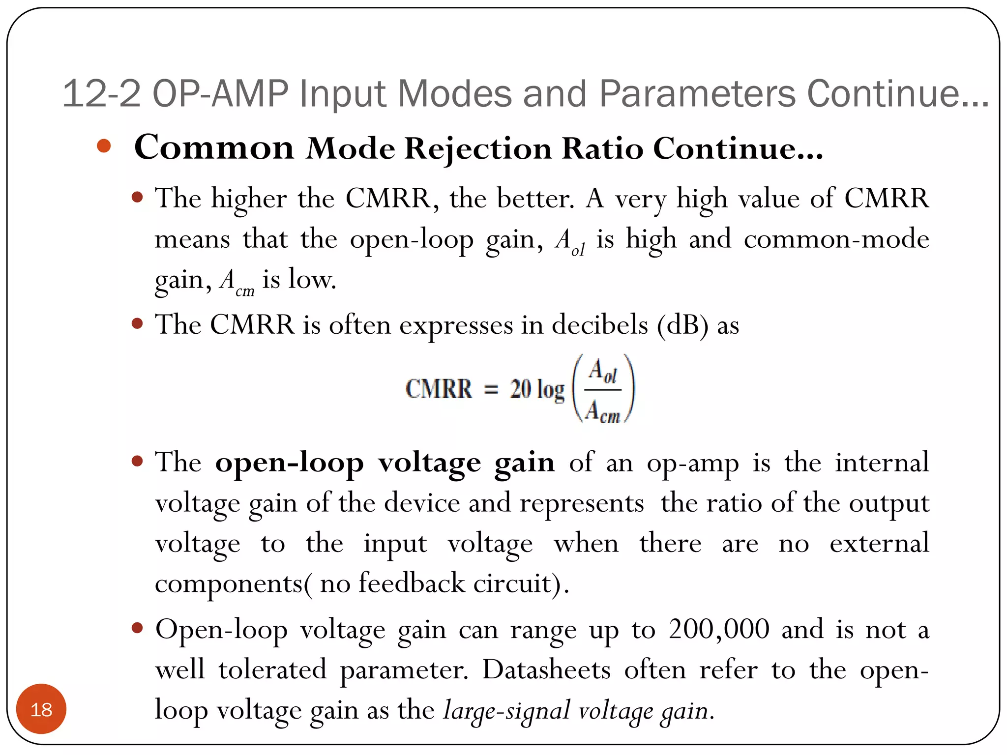
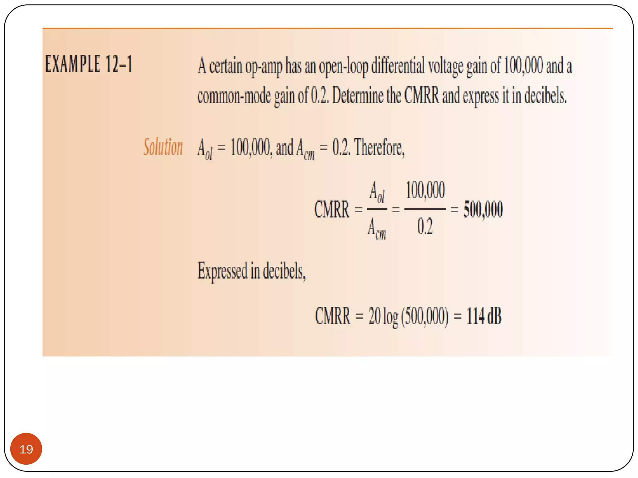

The document provides an introduction to operational amplifiers (op-amps), discussing their structure, function, and key characteristics including ideal versus practical limitations. It explores different modes of operation for differential amplifiers, input parameters, and the significance of negative feedback in controlling gain and stability. Additionally, the document details various parameters such as input impedance, common-mode rejection, and the concept of closed-loop voltage gain.


