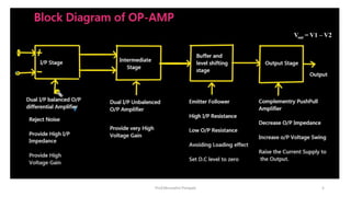
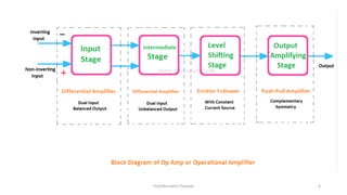
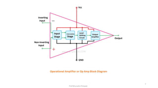
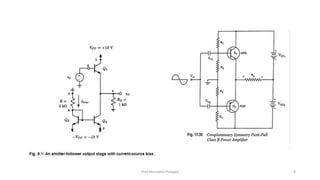
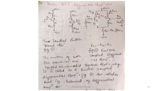
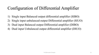
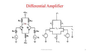
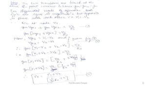
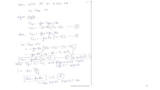
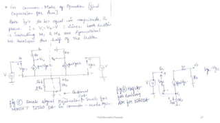
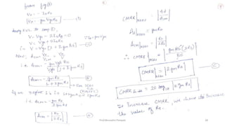
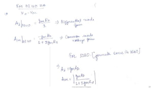
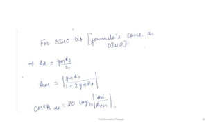
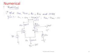
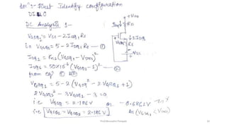
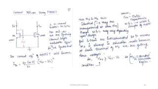
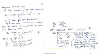
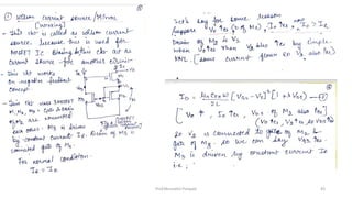
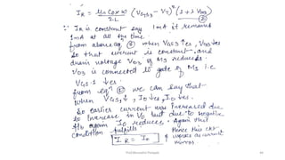
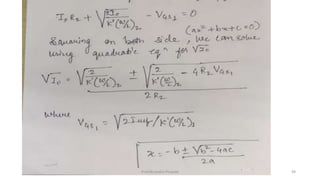
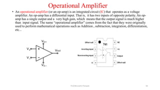
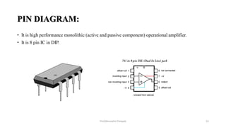
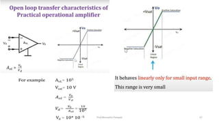
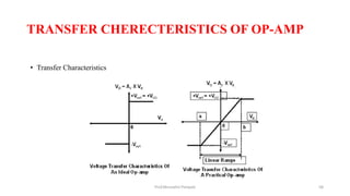
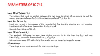
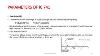
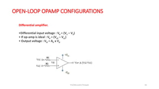
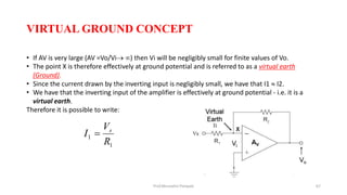
Integrated Circuits
Introduction to Operational Amplifier (Op-Amp)
Mrunalini Pimpale
Assistant Professor
Electronics and Telecommunication Engineering Department
Dwarkadas J. Sanghvi College of Engineering
Ville Parle-Mumbai
Prof.Mrunalini Pimpale
1
Operational Amplifier (Op-Amp)
Prof.Mrunalini Pimpale 2
• An operational amplifier (or an op-amp) is an integrated circuit (IC)
that operates as a voltage amplifier. An op-amp has a differential
input. That is, it has two inputs of opposite polarity. An op-amp has a
single output and a very high gain, which means that the output signal
is much higher than input signal.
Prof.Mrunalini Pimpale 3
Op-Amp Power Supply Connection
Vout = V1 – V2
Prof.Mrunalini Pimpale
1. Let V1= 5V and V2 = 3V then Vout = 5- 3 = 2V (Differential Mode)
2. Let V1= 5V and V2 = 5V then Vout = 5- 5 = 0V (Common Mode)
3. Let V1= 5V and V2 = 0 then Vout = 5- 0 = 5V (Single ended)
4. Let V1= 0V and V2 = 5V then Vout = 0-5 = -5V
4
Prof.Mrunalini Pimpale
Vout = V1 – V2
5
Prof.Mrunalini Pimpale 6
Prof.Mrunalini Pimpale
7
Prof.Mrunalini Pimpale 8
• First stage provides most of the voltage gain of op-amp and decides Ri
value
• Second stage is gain stage
• Third stage is level shifting stage:- Due to direct coupling between
first two stages, the input of level shifting stage is an amplified signal
with some non zero dc level. This stage is used to bring that dc level to
ground. In this stage the emitter follower with a constant current
source circuit is used.
• Last stage is a complementary output stage .This stage has
Complementary push pull power amplifier. It increases the magnitude
of the voltage and raises the current supplying capability of op-amp
along with low output resistance.
Prof.Mrunalini Pimpale 9
Differential Amplifier
Differential Amplifier is used to amplify the difference between the two
input signals. It is used in many Analog circuits. The input stage of
almost every Op-Amp is differential amplifier
Prof.Mrunalini Pimpale 10
Differential Amplifier:
Terminology and qualitative description:
1) Differential input voltage : (Vd)
If inputs (i.e Vin1 and Vin2) to differential amplifiers are such that there exists either amplitude or phase-
difference between them, then such input is known as “ differential input”
𝑉𝑑 = (𝑉𝑖𝑛1 − 𝑉𝑖𝑛2)
2) Differential mode gain: (Ad)
The gain with which differential amplifier amplifies differential input signal (Vd) is known as “ Differential mode gain”
𝐴𝑑 =
(𝑉𝑜1−𝑉𝑜2)
𝑉𝑑
=
(𝑉𝑜1−𝑉𝑜2)
(𝑣𝑖𝑛1−𝑉𝑖𝑛2)
=
𝑉𝑜
𝑉𝑑
Ideally, Ad ∞, Practically it should be large.
𝑉𝑜 = 𝑉𝑜1 − 𝑉𝑜2  Differential output voltage.
3) Common-mode input voltage : (VCM )
If input (i.e Vin1 and Vin2) to differential amplifier are of same magnitude and phase then
Such input is known as “Common mode input voltage”
𝑉𝑐𝑚 =
𝑉𝑖𝑛1+𝑉𝑖𝑛2
2
Prof.Mrunalini Pimpale 11
4) Common- mode gain : (ACM)
The gain with which differential amplifier amplifies common mode input signal is known as “Common mode gain”
𝐴𝑐𝑚 =
(𝑉𝑜𝑢𝑡)
𝑉𝑐𝑚
Ideally, Acm 0, Practically it should be very small.
Differential amplifier is designed to reject noise (common mode input), and to amplify differential mode signal
5) Common mode rejection ratio (CMRR)
 CMRR is a parameter which decides the ability of differential amplifier to reject (common mode signal) and amplify differential
mode signal.
 Mathematically , CMRR is the ratio of differential mode gain (Ad) to the common mode gain (Acm).
𝐶𝑀𝑅𝑅 =
|𝐴𝑑|
|𝐴𝑐𝑚|
𝐶𝑀𝑅𝑅 𝑖𝑛 𝑑𝑏 = 20 𝑙𝑜𝑔10
|𝐴𝑑|
|𝐴𝑐𝑚|
 Ideally, CMRR should be infinite (i.e Ad  ∞ and Acm  0 ) and practically it should be very high.
Prof.Mrunalini Pimpale 12
Features of Differential Amplifier:
1)High differential gain and low common mode gain.
2) High input impedance and low output impedance
3) High CMRR.
4) High gain.
5) Large Bandwidth
Prof.Mrunalini Pimpale 13
Prof.Mrunalini Pimpale 14
Configuration of Differential Amplifier
1) Single input Balanced output differential amplifier (SIBO)
2) Single input unbalanced output Differential amplifier (SIUO)
3) Dual input Balanced output Differential amplifier (DIBO)
4) Dual input Unbalanced output differential amplifier (DIUO)
Prof.Mrunalini Pimpale 15
Differential Amplifier
Prof.Mrunalini Pimpale 16
Single Input Unbalanced Output Single Input balanced Output
Dual Input unbalanced Output
Dual Input balanced Output
Prof.Mrunalini Pimpale 17
DC transfer characteristics of MOSFET Differential amplifier
Prof.Mrunalini Pimpale
EMOSFET Differential Amplifier
18
Prof.Mrunalini Pimpale 19
Prof.Mrunalini Pimpale 20
Why we always choose MOSFET DA?
• The maximum differential input signal for the MOSFET differential amplifier is
much larger than BJT differential amplifier.
• The primary reason is that the gain of the MOSFET differential amplifier , as we
will see, is much smaller than the gain of the BJT differential amplifier.
• Many DA are constructed with MOSFET’s since it provides high input
impedances, which helps amplifiers avoid loading of source.
• A MOSFET DA cannot provide high gain but it avoid loading of source.
• Also, MOSFET can be easily fabricated in IC form.
Prof.Mrunalini Pimpale 21
Dual input Balanced output Differential
Amplifier
• DC analysis
• AC analysis
Prof.Mrunalini Pimpale 22
Prof.Mrunalini Pimpale 23
Prof.Mrunalini Pimpale 24
Prof.Mrunalini Pimpale 25
Prof.Mrunalini Pimpale 26
Prof.Mrunalini Pimpale 27
Prof.Mrunalini Pimpale 28
Prof.Mrunalini Pimpale 29
Prof.Mrunalini Pimpale 30
Numerical
Prof.Mrunalini Pimpale 31
Prof.Mrunalini Pimpale 32
Prof.Mrunalini Pimpale 33
Prof.Mrunalini Pimpale 34
Active load can be used as current mirror circuit. Current mirror means we are copying the
same current from one device to other and main thing is we are controlling the current in
such way the main output current is not disturb , that is the constant
MOSFET Differential Amplifier with Active Load
Prof.Mrunalini Pimpale 35
Prof.Mrunalini Pimpale 36
Prof.Mrunalini Pimpale 37
Prof.Mrunalini Pimpale 38
Prof.Mrunalini Pimpale 39
MOSFET Differential Amplifier with Swamping
Resistor
• By using external resistors R’E in series with each emitter, the dependence of voltage gain on variations
of r’e can be reduced. It also increases the linearity range of the differential amplifier shows the
differential amplifier with swamping resistor R'E. The value of R'E is usually large enough to swamp the
effect of r’e.
Advantages of the swamping resistors is:
• Input resistance is high
• Increase the linearity range of the differential amplifier
• Minimization of the changes in the transistor parameters due to the temperature
Prof.Mrunalini Pimpale 40
Prof.Mrunalini Pimpale 41
Prof.Mrunalini Pimpale 42
Prof.Mrunalini Pimpale 43
Prof.Mrunalini Pimpale 44
Prof.Mrunalini Pimpale 45
Prof.Mrunalini Pimpale 46
Widlar Current Source:-
In basic Current mirror circuit when value of Iref = ID = low , then value of drain resistance
connected need to be increased, which is difficult to fabricate. Hence modifications are done in
the basic current mirror circuit as shown in figure called as WIDLAR Current Source
To avoid drawback of current mirror circuit Widlar Current source is used
Series resistance R2 is placed at source terminal of M2
It is suitable for low value currents
Used for generating low value currents, i.e. Io < IIN
Prof.Mrunalini Pimpale 47
Prof.Mrunalini Pimpale 48
Prof.Mrunalini Pimpale 49
Operational Amplifier
Prof.Mrunalini Pimpale
• An operational amplifier (or an op-amp) is an integrated circuit (IC) that operates as a voltage
amplifier. An op-amp has a differential input. That is, it has two inputs of opposite polarity. An op-
amp has a single output and a very high gain, which means that the output signal is much higher
than input signal. The name “operational amplifier” comes from the fact that they were originally
used to perform mathematical operations such as Addition , subtraction, integration, differentiation,
etc...
50
FEATURES:
• Null offset
• Excellent temperature stability
• High input voltage range
• Short circuit protection
• Low power consumption
Prof.Mrunalini Pimpale 51
PIN DIAGRAM:
• It is high performance monolithic (active and passive component) operational amplifier.
• It is 8 pin IC in DIP.
Prof.Mrunalini Pimpale 52
CHARACTERISTICS OF AN IDEAL OP-AMP
The ideal op-amp should have the following electrical characteristics:
• Infinite Voltage Gain (Av=∞)
• Infinite Input Resistance (Zin= ∞) so that any signal source can drive it and there is no
loading effect of preceding stage.
• Zero Output Resistance so that the output can drive an infinite number of other devices.
• Zero Offset Voltage when input is zero.
• Infinite CMRR (Common Mode Rejection Ratio) so that the output common mode noise
voltage is zero.
• Infinite Bandwidth (BW=∞) so that any frequency signal from 0 to ∞ Hz can be amplified
without attenuation.
• Infinite Slew Rate so that output voltage changes occur simultaneously with input voltage
changes.
Prof.Mrunalini Pimpale 53
IDEALAND PRACTICAL PARAMETERS OP-
AMP
Sr.No Characteristics Practical Value Ideal Value
1. Voltage Gain(A) 2x10⁵ ∞
2. Bandwidth(B.W) 1MHz ∞
3. CMRR(ρ) 90dB ∞
4. Input resi Ri 2M ohms ∞
5. Output resi. Ro 75 ohms 0
6. Slew Rate (S) 0.5 V/µs ∞
7. Input offset voltage (Vios) 2mV 0
8. PSRR 150µV/V 0
9. Input bias current IB 50nA 0
10. Input offset current Iios 6nA 0
Prof.Mrunalini Pimpale 54
EQUIVALENT CIRCUIT
Vo= Avid=A (v1-v2)
V1 & V2 - Input signals
Av - Voltage Gain
Ri - Input Resistance
R0 - Output Resistance
V0 - Output Voltage
Vd - Differential Input Voltage
Prof.Mrunalini Pimpale 55
Prof.Mrunalini Pimpale 56
Prof.Mrunalini Pimpale 57
TRANSFER CHERECTERISTICS OF OP-AMP
• Transfer Characteristics
Prof.Mrunalini Pimpale 58
PARAMETERS OF IC 741
Input Offset Voltage ( Vio)
• The voltage that must be applied between the two input terminals of an op-amp to null the
output as shown in figure. For 741C the maximum value of Vio is 6mv dc.
Input Bias Current (IB)
• Input bias current is the average of the currents that flow into the inverting and non inverting
input terminals of op-amp. In equation IB =(IB1 + IB2)/2
• Range is from 80 nA to 500 nA.
Input Offset Current (Iio)
• The algebraic difference between two biasing currents in to the inverting (IB2) and non
inverting(IB2) terminals. In equation form Iio =/IB1 - IB2/
• It is maximum value 200 nA for 741C.The smaller current shows better performance.
Offset voltage.
• The voltage across input terminals for zero output voltage.
Prof.Mrunalini Pimpale 59
PARAMETERS OF IC 741
• Slew Rate (SR)
• The maximum rate of change of output voltage per unit time in input frequency.
S=(dVo/ dt)/max Volts/microsecond
• It indicates how fast the output of op-amp can change in response to changes in input frequency.
High slew rate is desirable, for 741C , SR=0.5V/usec.
• Slew Rate Distortion:
• The picture above shows exactly what happens when the slew rate limitations are not met and
the output of the operational amplifier is distorted.
Prof.Mrunalini Pimpale 60
PARAMETERS OF IC 741
• Voltage Gain
• It is the ratio of the output voltage to the input voltage.
Av = Vo / Vd
For 741C op-amp voltage gain is A=200000.
• Common Mode Rejection Ratio (CMRR)
Ability of op-amp to reduce common mode I/p voltage or noise is known as CMRR, and
mathematically given by
CMRR=Ad/Ac
The CMRR should be as large as possible ideally infinite. For 741C CMRR is 90 dB.
• Power Supply Rejection Ratio (PSRR) or SVRR
PSRR=ΔVios /ΔV.
ΔVios: change in I/p offset voltage.
ΔV : change in supply voltage.
For 741C CMRR is150 uv/v.
Prof.Mrunalini Pimpale 61
PARAMETERS OF IC 741
• Output Signal swing (Vomax)
The output voltage swing of 741C op-amp is guaranteed to be between -13 and +13 V for RL>2KΩ
is 26 V Peak to peak voltage( undistorted ).The output never exceeds these limits for given supply
voltages +VCC and -VEE.
• Frequency Response:
Curve indicates change in voltage gain with frequency.
“The frequency at which voltage gain falls to unity is unity gain frequency.
• Supply current
For 741C current drawn by the op-amp from the power supply is Is=2.8mA.
Prof.Mrunalini Pimpale 62
OPEN-LOOP OP-AMP CONFIGURATIONS
•Inverting amplifier
•V1= 0 . For ideal op-amp, V2 = Vs
• Differential input voltage : Vd = (V1 – V2) = 0 – Vs = -Vs
• Output voltage : VO = AV x Vd = - AvVs
•Negative sign indicates a phase reversal or 180 degree phase shift
Prof.Mrunalini Pimpale 63
OPEN-LOOP OPAMP CONFIGURATIONS
• Noninverting amplifier
• V2 = 0 . For ideal op-amp, V1 = Vs
• Differential input voltage : Vd = (V1 – V2) = Vs – 0 = Vs
• Output voltage : VO = AV x Vd = AvVs
• No negative sign indicates absence of phase shift
Prof.Mrunalini Pimpale 64
OPEN-LOOP OPAMP CONFIGURATIONS
Differential amplifier.
•Differential input voltage : Vd = (V1 – V2)
• If op-amp is ideal : Vd = (Vs2 – Vs1)
• Output voltage : VO = AV x Vd
Prof.Mrunalini Pimpale 65
Limitation of openloop configurations
• The AC gain is not constant, Changes with supply, Changes with h-parameters,
and Age of device.
• The input and output impedances are not according to the requirement of the
basic amplifiers.
• Effect of distortion and noise is more.
• Bandwidth is not sufficiently large.
• These limitations are avoided by providing feedback.
Prof.Mrunalini Pimpale 66
VIRTUAL GROUND CONCEPT
• If AV is very large (AV =Vo/Vi ) then Vi will be negligibly small for finite values of Vo.
• The point X is therefore effectively at ground potential and is referred to as a virtual earth
(Ground).
• Since the current drawn by the inverting input is negligibly small, we have that I1  I2.
• We have that the inverting input of the amplifier is effectively at ground potential - i.e. it is a
virtual earth.
Therefore it is possible to write:
1
1
R
V
I s

Prof.Mrunalini Pimpale 67

Introduction to Operational Amplifier.pptx

  • 1.
    Integrated Circuits Introduction toOperational Amplifier (Op-Amp) Mrunalini Pimpale Assistant Professor Electronics and Telecommunication Engineering Department Dwarkadas J. Sanghvi College of Engineering Ville Parle-Mumbai Prof.Mrunalini Pimpale 1
  • 2.
  • 3.
    • An operationalamplifier (or an op-amp) is an integrated circuit (IC) that operates as a voltage amplifier. An op-amp has a differential input. That is, it has two inputs of opposite polarity. An op-amp has a single output and a very high gain, which means that the output signal is much higher than input signal. Prof.Mrunalini Pimpale 3
  • 4.
    Op-Amp Power SupplyConnection Vout = V1 – V2 Prof.Mrunalini Pimpale 1. Let V1= 5V and V2 = 3V then Vout = 5- 3 = 2V (Differential Mode) 2. Let V1= 5V and V2 = 5V then Vout = 5- 5 = 0V (Common Mode) 3. Let V1= 5V and V2 = 0 then Vout = 5- 0 = 5V (Single ended) 4. Let V1= 0V and V2 = 5V then Vout = 0-5 = -5V 4
  • 5.
  • 6.
  • 7.
  • 8.
  • 9.
    • First stageprovides most of the voltage gain of op-amp and decides Ri value • Second stage is gain stage • Third stage is level shifting stage:- Due to direct coupling between first two stages, the input of level shifting stage is an amplified signal with some non zero dc level. This stage is used to bring that dc level to ground. In this stage the emitter follower with a constant current source circuit is used. • Last stage is a complementary output stage .This stage has Complementary push pull power amplifier. It increases the magnitude of the voltage and raises the current supplying capability of op-amp along with low output resistance. Prof.Mrunalini Pimpale 9
  • 10.
    Differential Amplifier Differential Amplifieris used to amplify the difference between the two input signals. It is used in many Analog circuits. The input stage of almost every Op-Amp is differential amplifier Prof.Mrunalini Pimpale 10
  • 11.
    Differential Amplifier: Terminology andqualitative description: 1) Differential input voltage : (Vd) If inputs (i.e Vin1 and Vin2) to differential amplifiers are such that there exists either amplitude or phase- difference between them, then such input is known as “ differential input” 𝑉𝑑 = (𝑉𝑖𝑛1 − 𝑉𝑖𝑛2) 2) Differential mode gain: (Ad) The gain with which differential amplifier amplifies differential input signal (Vd) is known as “ Differential mode gain” 𝐴𝑑 = (𝑉𝑜1−𝑉𝑜2) 𝑉𝑑 = (𝑉𝑜1−𝑉𝑜2) (𝑣𝑖𝑛1−𝑉𝑖𝑛2) = 𝑉𝑜 𝑉𝑑 Ideally, Ad ∞, Practically it should be large. 𝑉𝑜 = 𝑉𝑜1 − 𝑉𝑜2  Differential output voltage. 3) Common-mode input voltage : (VCM ) If input (i.e Vin1 and Vin2) to differential amplifier are of same magnitude and phase then Such input is known as “Common mode input voltage” 𝑉𝑐𝑚 = 𝑉𝑖𝑛1+𝑉𝑖𝑛2 2 Prof.Mrunalini Pimpale 11
  • 12.
    4) Common- modegain : (ACM) The gain with which differential amplifier amplifies common mode input signal is known as “Common mode gain” 𝐴𝑐𝑚 = (𝑉𝑜𝑢𝑡) 𝑉𝑐𝑚 Ideally, Acm 0, Practically it should be very small. Differential amplifier is designed to reject noise (common mode input), and to amplify differential mode signal 5) Common mode rejection ratio (CMRR)  CMRR is a parameter which decides the ability of differential amplifier to reject (common mode signal) and amplify differential mode signal.  Mathematically , CMRR is the ratio of differential mode gain (Ad) to the common mode gain (Acm). 𝐶𝑀𝑅𝑅 = |𝐴𝑑| |𝐴𝑐𝑚| 𝐶𝑀𝑅𝑅 𝑖𝑛 𝑑𝑏 = 20 𝑙𝑜𝑔10 |𝐴𝑑| |𝐴𝑐𝑚|  Ideally, CMRR should be infinite (i.e Ad  ∞ and Acm  0 ) and practically it should be very high. Prof.Mrunalini Pimpale 12
  • 13.
    Features of DifferentialAmplifier: 1)High differential gain and low common mode gain. 2) High input impedance and low output impedance 3) High CMRR. 4) High gain. 5) Large Bandwidth Prof.Mrunalini Pimpale 13
  • 14.
  • 15.
    Configuration of DifferentialAmplifier 1) Single input Balanced output differential amplifier (SIBO) 2) Single input unbalanced output Differential amplifier (SIUO) 3) Dual input Balanced output Differential amplifier (DIBO) 4) Dual input Unbalanced output differential amplifier (DIUO) Prof.Mrunalini Pimpale 15
  • 16.
  • 17.
    Single Input UnbalancedOutput Single Input balanced Output Dual Input unbalanced Output Dual Input balanced Output Prof.Mrunalini Pimpale 17
  • 18.
    DC transfer characteristicsof MOSFET Differential amplifier Prof.Mrunalini Pimpale EMOSFET Differential Amplifier 18
  • 19.
  • 20.
  • 21.
    Why we alwayschoose MOSFET DA? • The maximum differential input signal for the MOSFET differential amplifier is much larger than BJT differential amplifier. • The primary reason is that the gain of the MOSFET differential amplifier , as we will see, is much smaller than the gain of the BJT differential amplifier. • Many DA are constructed with MOSFET’s since it provides high input impedances, which helps amplifiers avoid loading of source. • A MOSFET DA cannot provide high gain but it avoid loading of source. • Also, MOSFET can be easily fabricated in IC form. Prof.Mrunalini Pimpale 21
  • 22.
    Dual input Balancedoutput Differential Amplifier • DC analysis • AC analysis Prof.Mrunalini Pimpale 22
  • 23.
  • 24.
  • 25.
  • 26.
  • 27.
  • 28.
  • 29.
  • 30.
  • 31.
  • 32.
  • 33.
  • 34.
  • 35.
    Active load canbe used as current mirror circuit. Current mirror means we are copying the same current from one device to other and main thing is we are controlling the current in such way the main output current is not disturb , that is the constant MOSFET Differential Amplifier with Active Load Prof.Mrunalini Pimpale 35
  • 36.
  • 37.
  • 38.
  • 39.
  • 40.
    MOSFET Differential Amplifierwith Swamping Resistor • By using external resistors R’E in series with each emitter, the dependence of voltage gain on variations of r’e can be reduced. It also increases the linearity range of the differential amplifier shows the differential amplifier with swamping resistor R'E. The value of R'E is usually large enough to swamp the effect of r’e. Advantages of the swamping resistors is: • Input resistance is high • Increase the linearity range of the differential amplifier • Minimization of the changes in the transistor parameters due to the temperature Prof.Mrunalini Pimpale 40
  • 41.
  • 42.
  • 43.
  • 44.
  • 45.
  • 46.
  • 47.
    Widlar Current Source:- Inbasic Current mirror circuit when value of Iref = ID = low , then value of drain resistance connected need to be increased, which is difficult to fabricate. Hence modifications are done in the basic current mirror circuit as shown in figure called as WIDLAR Current Source To avoid drawback of current mirror circuit Widlar Current source is used Series resistance R2 is placed at source terminal of M2 It is suitable for low value currents Used for generating low value currents, i.e. Io < IIN Prof.Mrunalini Pimpale 47
  • 48.
  • 49.
  • 50.
    Operational Amplifier Prof.Mrunalini Pimpale •An operational amplifier (or an op-amp) is an integrated circuit (IC) that operates as a voltage amplifier. An op-amp has a differential input. That is, it has two inputs of opposite polarity. An op- amp has a single output and a very high gain, which means that the output signal is much higher than input signal. The name “operational amplifier” comes from the fact that they were originally used to perform mathematical operations such as Addition , subtraction, integration, differentiation, etc... 50
  • 51.
    FEATURES: • Null offset •Excellent temperature stability • High input voltage range • Short circuit protection • Low power consumption Prof.Mrunalini Pimpale 51
  • 52.
    PIN DIAGRAM: • Itis high performance monolithic (active and passive component) operational amplifier. • It is 8 pin IC in DIP. Prof.Mrunalini Pimpale 52
  • 53.
    CHARACTERISTICS OF ANIDEAL OP-AMP The ideal op-amp should have the following electrical characteristics: • Infinite Voltage Gain (Av=∞) • Infinite Input Resistance (Zin= ∞) so that any signal source can drive it and there is no loading effect of preceding stage. • Zero Output Resistance so that the output can drive an infinite number of other devices. • Zero Offset Voltage when input is zero. • Infinite CMRR (Common Mode Rejection Ratio) so that the output common mode noise voltage is zero. • Infinite Bandwidth (BW=∞) so that any frequency signal from 0 to ∞ Hz can be amplified without attenuation. • Infinite Slew Rate so that output voltage changes occur simultaneously with input voltage changes. Prof.Mrunalini Pimpale 53
  • 54.
    IDEALAND PRACTICAL PARAMETERSOP- AMP Sr.No Characteristics Practical Value Ideal Value 1. Voltage Gain(A) 2x10⁵ ∞ 2. Bandwidth(B.W) 1MHz ∞ 3. CMRR(ρ) 90dB ∞ 4. Input resi Ri 2M ohms ∞ 5. Output resi. Ro 75 ohms 0 6. Slew Rate (S) 0.5 V/µs ∞ 7. Input offset voltage (Vios) 2mV 0 8. PSRR 150µV/V 0 9. Input bias current IB 50nA 0 10. Input offset current Iios 6nA 0 Prof.Mrunalini Pimpale 54
  • 55.
    EQUIVALENT CIRCUIT Vo= Avid=A(v1-v2) V1 & V2 - Input signals Av - Voltage Gain Ri - Input Resistance R0 - Output Resistance V0 - Output Voltage Vd - Differential Input Voltage Prof.Mrunalini Pimpale 55
  • 56.
  • 57.
  • 58.
    TRANSFER CHERECTERISTICS OFOP-AMP • Transfer Characteristics Prof.Mrunalini Pimpale 58
  • 59.
    PARAMETERS OF IC741 Input Offset Voltage ( Vio) • The voltage that must be applied between the two input terminals of an op-amp to null the output as shown in figure. For 741C the maximum value of Vio is 6mv dc. Input Bias Current (IB) • Input bias current is the average of the currents that flow into the inverting and non inverting input terminals of op-amp. In equation IB =(IB1 + IB2)/2 • Range is from 80 nA to 500 nA. Input Offset Current (Iio) • The algebraic difference between two biasing currents in to the inverting (IB2) and non inverting(IB2) terminals. In equation form Iio =/IB1 - IB2/ • It is maximum value 200 nA for 741C.The smaller current shows better performance. Offset voltage. • The voltage across input terminals for zero output voltage. Prof.Mrunalini Pimpale 59
  • 60.
    PARAMETERS OF IC741 • Slew Rate (SR) • The maximum rate of change of output voltage per unit time in input frequency. S=(dVo/ dt)/max Volts/microsecond • It indicates how fast the output of op-amp can change in response to changes in input frequency. High slew rate is desirable, for 741C , SR=0.5V/usec. • Slew Rate Distortion: • The picture above shows exactly what happens when the slew rate limitations are not met and the output of the operational amplifier is distorted. Prof.Mrunalini Pimpale 60
  • 61.
    PARAMETERS OF IC741 • Voltage Gain • It is the ratio of the output voltage to the input voltage. Av = Vo / Vd For 741C op-amp voltage gain is A=200000. • Common Mode Rejection Ratio (CMRR) Ability of op-amp to reduce common mode I/p voltage or noise is known as CMRR, and mathematically given by CMRR=Ad/Ac The CMRR should be as large as possible ideally infinite. For 741C CMRR is 90 dB. • Power Supply Rejection Ratio (PSRR) or SVRR PSRR=ΔVios /ΔV. ΔVios: change in I/p offset voltage. ΔV : change in supply voltage. For 741C CMRR is150 uv/v. Prof.Mrunalini Pimpale 61
  • 62.
    PARAMETERS OF IC741 • Output Signal swing (Vomax) The output voltage swing of 741C op-amp is guaranteed to be between -13 and +13 V for RL>2KΩ is 26 V Peak to peak voltage( undistorted ).The output never exceeds these limits for given supply voltages +VCC and -VEE. • Frequency Response: Curve indicates change in voltage gain with frequency. “The frequency at which voltage gain falls to unity is unity gain frequency. • Supply current For 741C current drawn by the op-amp from the power supply is Is=2.8mA. Prof.Mrunalini Pimpale 62
  • 63.
    OPEN-LOOP OP-AMP CONFIGURATIONS •Invertingamplifier •V1= 0 . For ideal op-amp, V2 = Vs • Differential input voltage : Vd = (V1 – V2) = 0 – Vs = -Vs • Output voltage : VO = AV x Vd = - AvVs •Negative sign indicates a phase reversal or 180 degree phase shift Prof.Mrunalini Pimpale 63
  • 64.
    OPEN-LOOP OPAMP CONFIGURATIONS •Noninverting amplifier • V2 = 0 . For ideal op-amp, V1 = Vs • Differential input voltage : Vd = (V1 – V2) = Vs – 0 = Vs • Output voltage : VO = AV x Vd = AvVs • No negative sign indicates absence of phase shift Prof.Mrunalini Pimpale 64
  • 65.
    OPEN-LOOP OPAMP CONFIGURATIONS Differentialamplifier. •Differential input voltage : Vd = (V1 – V2) • If op-amp is ideal : Vd = (Vs2 – Vs1) • Output voltage : VO = AV x Vd Prof.Mrunalini Pimpale 65
  • 66.
    Limitation of openloopconfigurations • The AC gain is not constant, Changes with supply, Changes with h-parameters, and Age of device. • The input and output impedances are not according to the requirement of the basic amplifiers. • Effect of distortion and noise is more. • Bandwidth is not sufficiently large. • These limitations are avoided by providing feedback. Prof.Mrunalini Pimpale 66
  • 67.
    VIRTUAL GROUND CONCEPT •If AV is very large (AV =Vo/Vi ) then Vi will be negligibly small for finite values of Vo. • The point X is therefore effectively at ground potential and is referred to as a virtual earth (Ground). • Since the current drawn by the inverting input is negligibly small, we have that I1  I2. • We have that the inverting input of the amplifier is effectively at ground potential - i.e. it is a virtual earth. Therefore it is possible to write: 1 1 R V I s  Prof.Mrunalini Pimpale 67