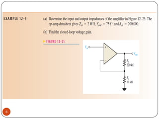
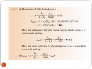
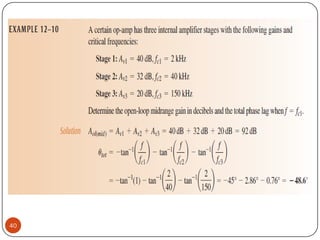
Downloaded 328 times

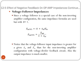
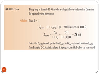
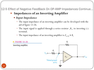
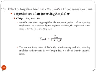
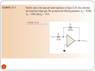
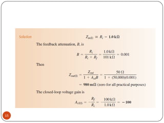
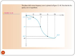
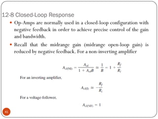
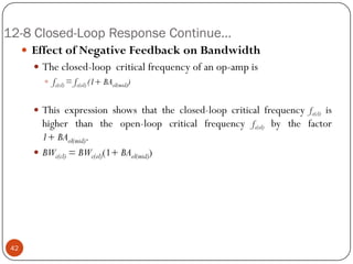
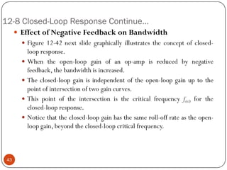
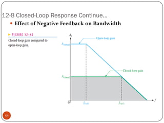
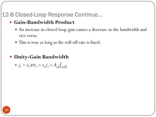
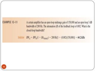
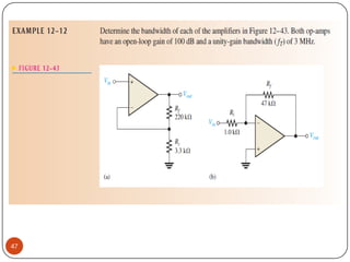
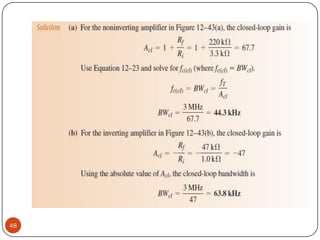

The document discusses the operational amplifier (op-amp) focusing on the effects of negative feedback on input and output impedances for both non-inverting and inverting amplifier configurations. It explains concepts like input bias current, offset voltage, open-loop and closed-loop responses, and emphasizes how negative feedback influences bandwidth and gain. Additionally, it details compensation techniques for bias currents and their impact on the overall performance of op-amps.