Downloaded 303 times
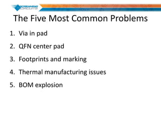
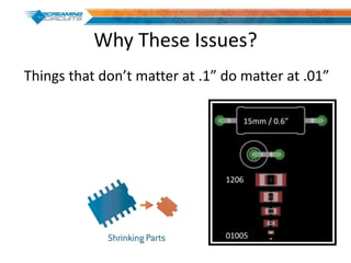
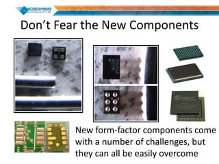
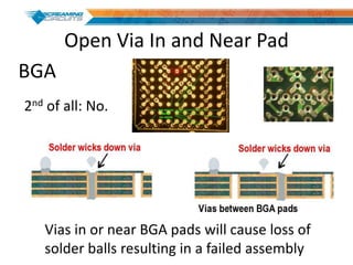
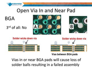
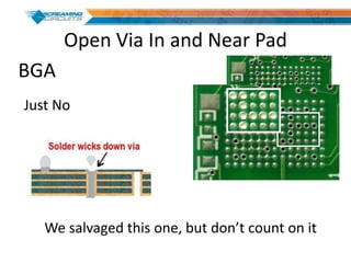
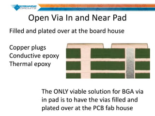
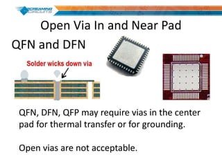
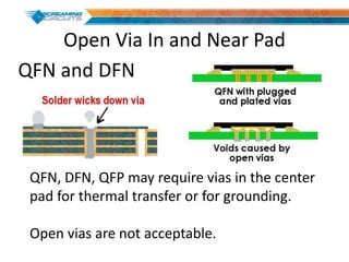
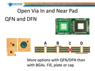
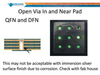
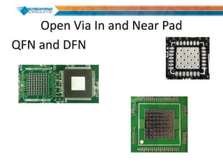
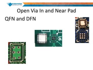
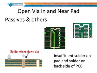
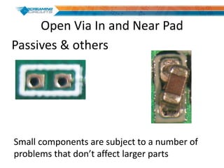
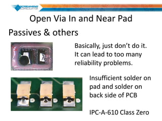

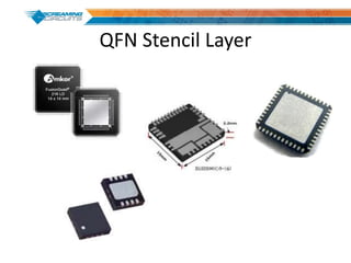
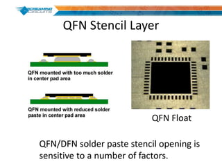
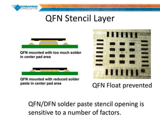
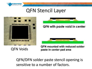
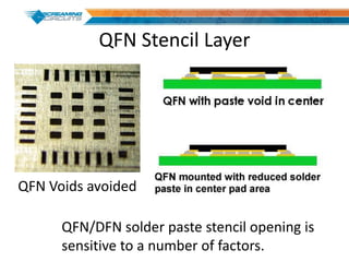
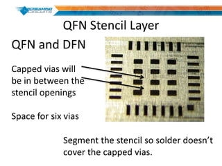
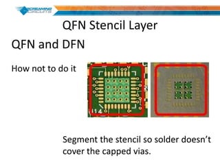
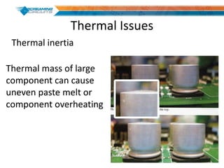
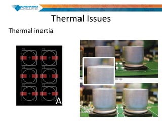
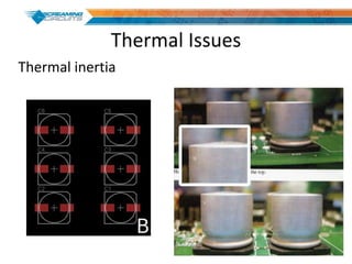
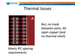
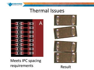
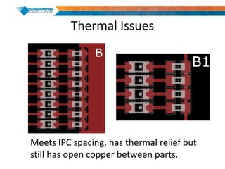
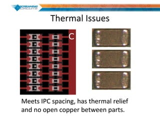
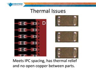
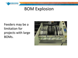
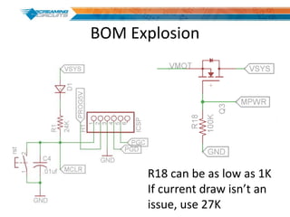

This document discusses best practices for PCB design to improve manufacturing reliability. It identifies five common problems: 1) via in pad, 2) QFN center pad issues, 3) incorrect footprints and markings, 4) thermal manufacturing issues, and 5) bill of materials explosions. Each issue is explained in detail with examples of both correct and incorrect design approaches. The document emphasizes that aspects that don't impact larger boards can cause failures at smaller scales, and provides tips for via filling, stencil segmentation, thermal relief, and managing component counts.


![ppt[1].pptx, different types of cables, stages of testing](https://cdn.slidesharecdn.com/ss_thumbnails/lotusppt1-251225085754-c6f0df1c-thumbnail.jpg?width=640&height=640&fit=bounds)