
![About :
• Strategic
Consul8ng,
including
business
plan
&
sales
strategy
development
for
high
technology
products,
acquisi8ons
and
partnership.
•
Proposal
support,
cri8que,
evalua8on
and
genera8on
• Failure
analysis
of
thin
film
and
thick
film
resistors,
integrated
circuits
and
board
level
problems
• Electronic
Design
engineering
and
so]ware
support
• Technology
review
and
research
for
consumer
electronics,
internet
devices,
solar
energy,
MEMS,
nanotechnology,
microelectronics,
SMT,
and
health
care
so]ware
products.
32](https://image.slidesharecdn.com/electronicpackagingtrendshort1032011-13190316439308-phpapp02-111019084149-phpapp02/85/Electronic-Packaging-Trend-Short-10-3-2011-32-320.jpg)

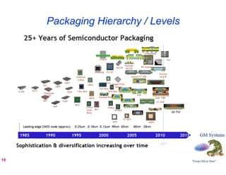
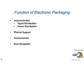
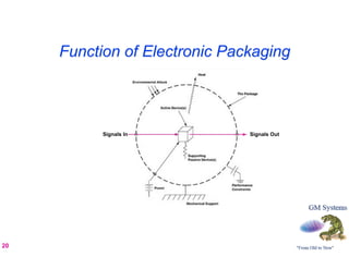
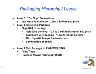
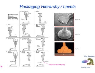
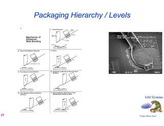
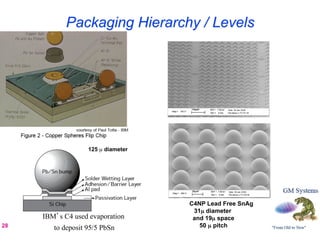
This document discusses electronic packaging trends. It provides a brief history of electronic packaging from the transistor to modern technologies like 3D stacking. It describes the hierarchy of packaging from the chip level to board and system levels. Recent trends include advanced packaging for mobile devices and future technologies like 3D integration. The document aims to provide an overview of electronic packaging and sources for further study.


