William Stallings
Computer Organization
and Architecture
7th Edition
Chapter 5
Internal Memory
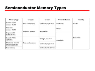
Semiconductor Memory Types
Semiconductor Memory
• RAM
—Misnamed as all semiconductor memory is
random access
—Read/Write
—Volatile
—Temporary storage
—Static or dynamic
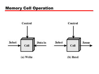
Memory Cell Operation
Dynamic RAM
• Bits stored as charge in capacitors
• Charges leak
• Need refreshing even when powered
• Simpler construction
• Smaller per bit
• Less expensive
• Need refresh circuits
• Slower
• Main memory
• Essentially analogue
—Level of charge determines value
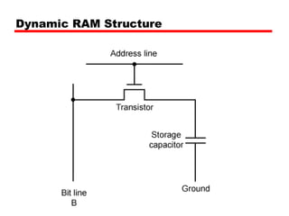
Dynamic RAM Structure
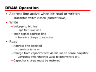
DRAM Operation
• Address line active when bit read or written
—Transistor switch closed (current flows)
• Write
—Voltage to bit line
– High for 1 low for 0
—Then signal address line
– Transfers charge to capacitor
• Read
—Address line selected
– transistor turns on
—Charge from capacitor fed via bit line to sense amplifier
– Compares with reference value to determine 0 or 1
—Capacitor charge must be restored
Static RAM
• Bits stored as on/off switches
• No charges to leak
• No refreshing needed when powered
• More complex construction
• Larger per bit
• More expensive
• Does not need refresh circuits
• Faster
• Cache
• Digital
—Uses flip-flops
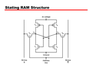
Stating RAM Structure
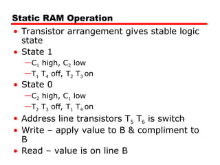
Static RAM Operation
• Transistor arrangement gives stable logic
state
• State 1
—C1 high, C2 low
—T1 T4 off, T2 T3 on
• State 0
—C2 high, C1 low
—T2 T3 off, T1 T4 on
• Address line transistors T5 T6 is switch
• Write – apply value to B & compliment to
B
• Read – value is on line B
SRAM v DRAM
• Both volatile
—Power needed to preserve data
• Dynamic cell
—Simpler to build, smaller
—More dense
—Less expensive
—Needs refresh
—Larger memory units
• Static
—Faster
—Cache
Read Only Memory (ROM)
• Permanent storage
—Nonvolatile
• Microprogramming (see later)
• Library subroutines
• Systems programs (BIOS)
• Function tables
Types of ROM
• Written during manufacture
—Very expensive for small runs
• Programmable (once)
—PROM
—Needs special equipment to program
• Read “mostly”
—Erasable Programmable (EPROM)
– Erased by UV
—Electrically Erasable (EEPROM)
– Takes much longer to write than read
—Flash memory
– Erase whole memory electrically
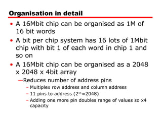
Organisation in detail
• A 16Mbit chip can be organised as 1M of
16 bit words
• A bit per chip system has 16 lots of 1Mbit
chip with bit 1 of each word in chip 1 and
so on
• A 16Mbit chip can be organised as a 2048
x 2048 x 4bit array
—Reduces number of address pins
– Multiplex row address and column address
– 11 pins to address (211
=2048)
– Adding one more pin doubles range of values so x4
capacity
Refreshing
• Refresh circuit included on chip
• Disable chip
• Count through rows
• Read & Write back
• Takes time
• Slows down apparent performance
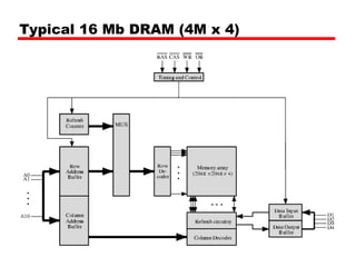
Typical 16 Mb DRAM (4M x 4)
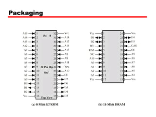
Packaging
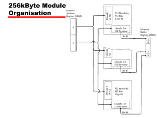
256kByte Module
Organisation
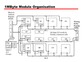
1MByte Module Organisation
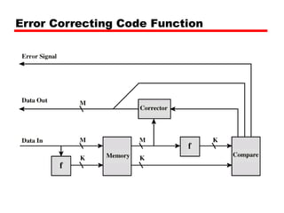
Error Correction
• Hard Failure
—Permanent defect
• Soft Error
—Random, non-destructive
—No permanent damage to memory
• Detected using Hamming error correcting
code
Error Correcting Code Function
Advanced DRAM Organization
• Basic DRAM same since first RAM chips
• Enhanced DRAM
—Contains small SRAM as well
—SRAM holds last line read (c.f. Cache!)
• Cache DRAM
—Larger SRAM component
—Use as cache or serial buffer
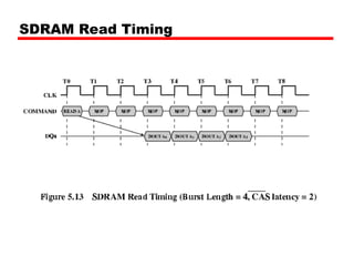
Synchronous DRAM (SDRAM)
• Access is synchronized with an external clock
• Address is presented to RAM
• RAM finds data (CPU waits in conventional
DRAM)
• Since SDRAM moves data in time with system
clock, CPU knows when data will be ready
• CPU does not have to wait, it can do something
else
• Burst mode allows SDRAM to set up stream of
data and fire it out in block
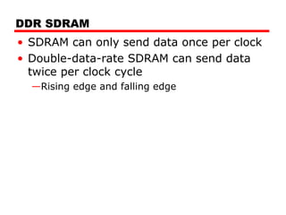
• DDR-SDRAM sends data twice per clock cycle
(leading & trailing edge)
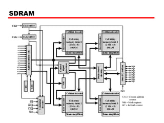
SDRAM
SDRAM Read Timing
RAMBUS
• Adopted by Intel for Pentium & Itanium
• Main competitor to SDRAM
• Vertical package – all pins on one side
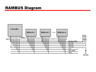
• Data exchange over 28 wires < cm long
• Bus addresses up to 320 RDRAM chips at
1.6Gbps
• Asynchronous block protocol
—480ns access time
—Then 1.6 Gbps
RAMBUS Diagram
DDR SDRAM
• SDRAM can only send data once per clock
• Double-data-rate SDRAM can send data
twice per clock cycle
—Rising edge and falling edge
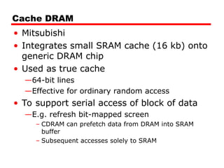
Cache DRAM
• Mitsubishi
• Integrates small SRAM cache (16 kb) onto
generic DRAM chip
• Used as true cache
—64-bit lines
—Effective for ordinary random access
• To support serial access of block of data
—E.g. refresh bit-mapped screen
– CDRAM can prefetch data from DRAM into SRAM
buffer
– Subsequent accesses solely to SRAM
Reading
• The RAM Guide
• RDRAM

SRAM- DRAM Structure Internal Memory.ppt

  • 1.
    William Stallings Computer Organization andArchitecture 7th Edition Chapter 5 Internal Memory
  • 2.
  • 3.
    Semiconductor Memory • RAM —Misnamedas all semiconductor memory is random access —Read/Write —Volatile —Temporary storage —Static or dynamic
  • 4.
  • 5.
    Dynamic RAM • Bitsstored as charge in capacitors • Charges leak • Need refreshing even when powered • Simpler construction • Smaller per bit • Less expensive • Need refresh circuits • Slower • Main memory • Essentially analogue —Level of charge determines value
  • 6.
  • 7.
    DRAM Operation • Addressline active when bit read or written —Transistor switch closed (current flows) • Write —Voltage to bit line – High for 1 low for 0 —Then signal address line – Transfers charge to capacitor • Read —Address line selected – transistor turns on —Charge from capacitor fed via bit line to sense amplifier – Compares with reference value to determine 0 or 1 —Capacitor charge must be restored
  • 8.
    Static RAM • Bitsstored as on/off switches • No charges to leak • No refreshing needed when powered • More complex construction • Larger per bit • More expensive • Does not need refresh circuits • Faster • Cache • Digital —Uses flip-flops
  • 9.
  • 10.
    Static RAM Operation •Transistor arrangement gives stable logic state • State 1 —C1 high, C2 low —T1 T4 off, T2 T3 on • State 0 —C2 high, C1 low —T2 T3 off, T1 T4 on • Address line transistors T5 T6 is switch • Write – apply value to B & compliment to B • Read – value is on line B
  • 11.
    SRAM v DRAM •Both volatile —Power needed to preserve data • Dynamic cell —Simpler to build, smaller —More dense —Less expensive —Needs refresh —Larger memory units • Static —Faster —Cache
  • 12.
    Read Only Memory(ROM) • Permanent storage —Nonvolatile • Microprogramming (see later) • Library subroutines • Systems programs (BIOS) • Function tables
  • 13.
    Types of ROM •Written during manufacture —Very expensive for small runs • Programmable (once) —PROM —Needs special equipment to program • Read “mostly” —Erasable Programmable (EPROM) – Erased by UV —Electrically Erasable (EEPROM) – Takes much longer to write than read —Flash memory – Erase whole memory electrically
  • 14.
    Organisation in detail •A 16Mbit chip can be organised as 1M of 16 bit words • A bit per chip system has 16 lots of 1Mbit chip with bit 1 of each word in chip 1 and so on • A 16Mbit chip can be organised as a 2048 x 2048 x 4bit array —Reduces number of address pins – Multiplex row address and column address – 11 pins to address (211 =2048) – Adding one more pin doubles range of values so x4 capacity
  • 15.
    Refreshing • Refresh circuitincluded on chip • Disable chip • Count through rows • Read & Write back • Takes time • Slows down apparent performance
  • 16.
    Typical 16 MbDRAM (4M x 4)
  • 17.
  • 18.
  • 19.
  • 20.
    Error Correction • HardFailure —Permanent defect • Soft Error —Random, non-destructive —No permanent damage to memory • Detected using Hamming error correcting code
  • 21.
  • 22.
    Advanced DRAM Organization •Basic DRAM same since first RAM chips • Enhanced DRAM —Contains small SRAM as well —SRAM holds last line read (c.f. Cache!) • Cache DRAM —Larger SRAM component —Use as cache or serial buffer
  • 23.
    Synchronous DRAM (SDRAM) •Access is synchronized with an external clock • Address is presented to RAM • RAM finds data (CPU waits in conventional DRAM) • Since SDRAM moves data in time with system clock, CPU knows when data will be ready • CPU does not have to wait, it can do something else • Burst mode allows SDRAM to set up stream of data and fire it out in block • DDR-SDRAM sends data twice per clock cycle (leading & trailing edge)
  • 24.
  • 25.
  • 26.
    RAMBUS • Adopted byIntel for Pentium & Itanium • Main competitor to SDRAM • Vertical package – all pins on one side • Data exchange over 28 wires < cm long • Bus addresses up to 320 RDRAM chips at 1.6Gbps • Asynchronous block protocol —480ns access time —Then 1.6 Gbps
  • 27.
  • 28.
    DDR SDRAM • SDRAMcan only send data once per clock • Double-data-rate SDRAM can send data twice per clock cycle —Rising edge and falling edge
  • 29.
    Cache DRAM • Mitsubishi •Integrates small SRAM cache (16 kb) onto generic DRAM chip • Used as true cache —64-bit lines —Effective for ordinary random access • To support serial access of block of data —E.g. refresh bit-mapped screen – CDRAM can prefetch data from DRAM into SRAM buffer – Subsequent accesses solely to SRAM
  • 30.
    Reading • The RAMGuide • RDRAM