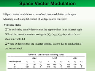
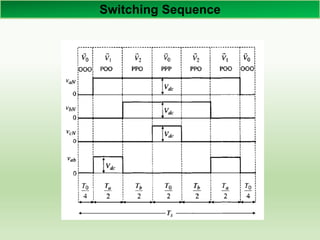
![Space Vector
Space Vectors
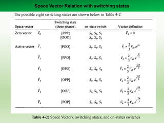
Among the eight switching
states, [PPP] and [OOO] are
zero states and the others are
called active states.
The active and zero
switching states can be
represented by active and zero
vectors, respectively.
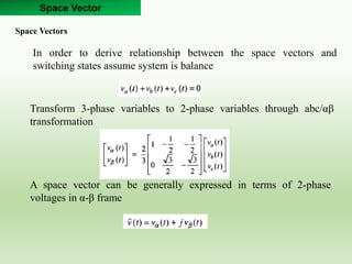
Space vector diagram for
two-level inverter is shown
Six vectors V1 to V6 form
hexagon with six equal sectors
and zero vector V0 lies in
center of hexagon](https://image.slidesharecdn.com/spvm-140605022805-phpapp01/85/Sinusoidal-PWM-and-Space-Vector-Modulation-For-Two-Level-Voltage-Source-Converter-13-320.jpg)

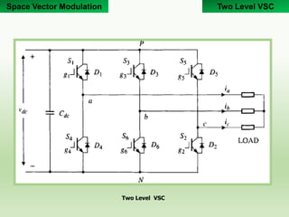
![Space Vector
+
VDC
-
Vb
Va
Vc
S1 S3 S5
S4 S6 S2
N
R
R R
N
Vdc
3
2
Vdc
3
1
Vdc
3
1
For [POO] the Equivalent Circuit](https://image.slidesharecdn.com/spvm-140605022805-phpapp01/85/Sinusoidal-PWM-and-Space-Vector-Modulation-For-Two-Level-Voltage-Source-Converter-17-320.jpg)


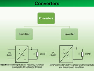
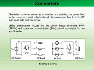
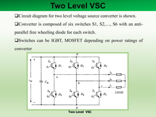
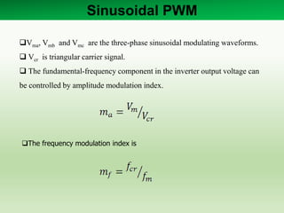
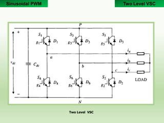
1) The document describes a two level voltage source converter (VSC) that can operate as either a rectifier or inverter using carrier-based sinusoidal pulse width modulation (PWM) or space vector modulation (SVM) control techniques. 2) The two level VSC consists of six switches that can be IGBTs or MOSFETs with anti-parallel diodes, allowing bidirectional power flow between the DC and AC sides. 3) Sinusoidal PWM compares a triangular carrier signal to three-phase modulating waves to generate switching pulses for the converter switches, while SVM represents the converter states as space vectors to calculate switching times.