Downloaded 4,010 times
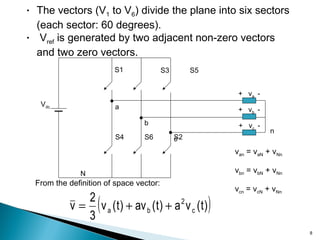
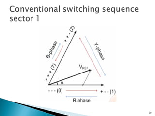
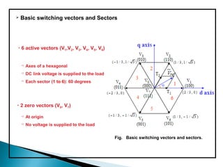
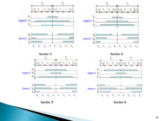
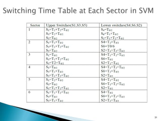
![Sector 1Sector 3
Sector 4
Sector 5
Sector 2
Sector 6
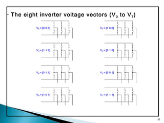
[100] V1
[110] V2[010] V3
[011] V4
[001] V5 [101] V6
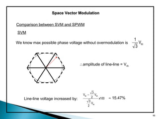
(2/3)Vdc
(1/√3)Vdc
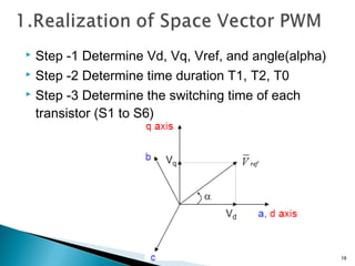
Space Vector ModulationSpace Vector Modulation
( )c
2
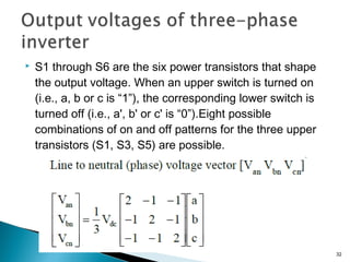
badc SaaSSV
3
2
v ++=
14](https://image.slidesharecdn.com/svpwmpptproject-150430100442-conversion-gate01/85/Space-Vector-Modulation-SVM-Technique-for-PWM-Inverter-14-320.jpg)
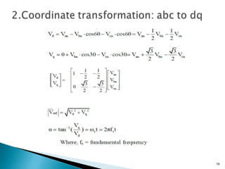
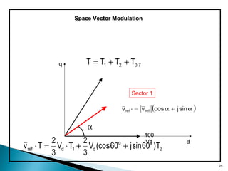
![Space Vector ModulationSpace Vector Modulation
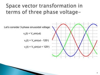
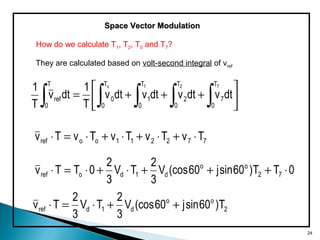
Solving for T1, T2 and T0,7 gives:
2
oo
d1dref T)60sinj60(cosV
3
2
TV
3
2
Tv ++⋅=⋅
2d1dref TV
3
1
TV
3
2
cosvT +=α 2dref TV
3
1
sinvT =α
T1= 3/2 m[ (T/√3) cos α - (1/3)T sin α ]
T2= mT sin α
where,
M= Vref/ (Vd/ √3)
26](https://image.slidesharecdn.com/svpwmpptproject-150430100442-conversion-gate01/85/Space-Vector-Modulation-SVM-Technique-for-PWM-Inverter-26-320.jpg)
![1[1]. Hind Djeghloud and Hocine Benalla, “Space Vector Pulse Width Modulation
Applied to The Three-Level Voltage Inverter”, 5th International Conference on
Technology and Automation ICTA’05, Thessaloniki, Greece, Oct 2010.
[2]. Jin-woo Jung, “Space Vector PWM Inverter”, The Ohio State University, February,
2008.
[3]. Jae Hyeong Seo; Chang Ho Choi; Dong Seok Hyun, “A New Simplified space-
Vector PWM Method for Three-Level Inverters”, IEEE Transactions on Power
Electronics, Volume 16, Issue 4, Jul 2010, Pages 545 - 550
[4]. Muhammad H.Rashid “Power Electronics Circuits, devices, and Applications”,
Prentice-Hall of India Private Limited, Third Edition, 2004.
[5]. “the adaptive space vector pwm for four switch three phase inverter fed induction
motor with dc – link voltage imbalance” by Hong Hee Lee*, Phan Quoc Dzung**, Le
Dinh Khoa**, Le Minh Phuong**, Huynh Tan Thanh***School of Electrical Engineering,
University of Ulsan Ulsan, Korea.
[6]. P.S.Bimbhra, “Power Electronics”, Khanna publications.
[7]. Overview of MATLAB Simulink
Http://www.mathworks.com/products/simulink/description/overview.shtml
49](https://image.slidesharecdn.com/svpwmpptproject-150430100442-conversion-gate01/85/Space-Vector-Modulation-SVM-Technique-for-PWM-Inverter-49-320.jpg)


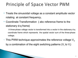
This document discusses space vector pulse width modulation (SVM) for three-phase voltage source inverters. It begins by introducing SVM and its benefits over other PWM techniques, such as reduced total harmonic distortion. It then provides details on how SVM works, including transforming a three-phase reference signal to a rotating vector in the d-q reference frame. The document explains the eight possible switching states, sectors, and how to calculate switching times to synthesize the reference signal using adjacent active vectors and zero vectors. It concludes by comparing SVM to sinusoidal PWM, showing SVM offers better voltage utilization and harmonic performance.


![[Deck] What's New in Spark-Iceberg Integration via DSV2.pptx](https://cdn.slidesharecdn.com/ss_thumbnails/deckwhatsnewinspark-icebergintegrationviadsv2-260210005337-25955b12-thumbnail.jpg?width=640&height=640&fit=bounds)


