The document analyzes the conduction modes and efficiency of buck-boost, buck, and boost power converters. Simulation results show that continuous conduction mode (CCM) has the highest efficiency for all three converters. For a given duty cycle, increasing the inductor value decreases the peak-to-peak ripple. The conduction mode can also be varied by keeping the inductance constant and changing the duty cycle, which keeps the ripple value the same. Therefore, the filter is designed for a specific inductance value. Tables of results are presented comparing efficiency for different conduction modes under varying duty cycles and inductance values.
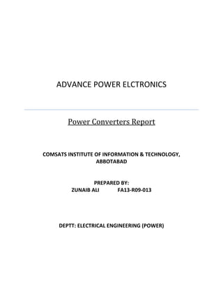
Space Vector Pulse Width Modulation Technique Applied to Two Level Voltage So...Qusai Abdelrahman
Space vector pulse width modulation SVPWM provides a better technique compared to the other pulse width modulation techniques. This paper presents simulation and implementation of SVPWM signal generation for driving three phase two level voltage source inverter VSI, also proposes and analyzes a new switching sequence for generating an SVPWM. Simulation results are obtained using the simulation package PSIM. and the inverter performance is evaluated in terms of total harmonic distortion (THD). The model is experimentally implemented and verified on Arduino Mega Atmega2560 microcontroller.
Sinusoidal PWM and Space Vector Modulation For Two Level Voltage Source Conve...ZunAib Ali
Complete detail of Sinusoidal PWM and Space Vector Modulation For Two Level Voltage Source Converter
Space Vector Modulation includes:
Switching states, space vector, space vector diagram, space vector and switching states relationship, Dwell time, switching sequence
Space Vector Pulse Width Modulation Schemes for Two-Level Voltage Source Inve...IDES Editor
Space Vector Pulse Width Modulation (SVPWM)
method is an advanced, computation intensive PWM method
and possibly the best among all the PWM techniques for
variable frequency drive applications. The SVPWM is an
alternative method for the determination of switching pulse
width and their position. The major advantage of SVPWM
stem from the fact that, there is a degree of freedom of space
vector placement in a switching cycle. This feature improves
the harmonic performance of this method. This method has
been finding widespread application in recent years because
of the easier digital realization and better dc bus utilization.
In this paper, three SVPWM schemes, called 7-segment space
vector modulation (SVM), 7-segment SVM with even-order
harmonic elimination and 5-segment (discontinuous) SVM
are studied in detail. The theoretical analysis, design,
switching sequence and SIMULINK implementation of these
three SVM schemes is presented in step-by-step manner
Space Vector PWM (SVPWM) is a more sophisticated technique for generating a fundamental sine wave that provides a higher voltage to the motor and lower total harmonic distortion (THD).
Study of sinusoidal and space vector pulse width modulation techniques for a ...eSAT Journals
Abstract
This paper compares and evaluates the performance of Sinusoidal Pulse Width Modulation (SPWM) and Space Vector Pulse Width
Modulation (SVPWM) techniques for a three-level inverter by cascading two two-level inverters. In this topology, four power
semiconductor switches are used per phase and a total of twelve switches are required. The simulation study shows that SVPWM is
superior to SPWM in the aspects of better DC-bus utilization and offering better spectral performance.
Index Terms: space vector modulation, multi-level inverters, sine-triangle modulation, and cascaded inverter
Harmonic comparisons of various PWM techniques for basic MLISaquib Maqsood
Cascaded inverters are ideal for connecting renewable energy sources with an AC grid, because of the need for separate dc sources, which is the case in applications such as photovoltaic or fuel cells. The inverter could be controlled to either regulate the power factor of the current drawn from the source or the bus voltage of the electrical system where the inverter was connected. The modulation techniques are crucial in operating any inverter at desired conditions. In this work different PWM techniques are implemented for five level cascaded multilevel inverter and THD variation is analyzed.
Two leg three-phase inverters (FSTPIs) have been proposed to be used in low-power; low-cost applications because of the reduced number of semiconductor devices, and space vector pulse width modulation (SVPWM) techniques have also been introduced to control FSTPIs. However, high-performance controllers are needed to implement complicated SVPWM algorithms, which limit their low-cost applications. To simplify algorithms and reduce the cost of implementation, an equivalent scalar method for SVPWM of FSTPIs is proposed. SVPWM for FSTPIs is actually a sine PWM by modulating two sine waves of 600 phase difference with a triangle wave, but in this method third harmonics doesn’t eliminated. So as to eliminate the third harmonics we have to compose a high frequency sine wave to on existing sine waves. So such a special sine PWM can be used to control FSTPIs. The Mathematical and simulation results demonstrate the validity of the proposed method.
http://www.mathworks.com/matlabcentral/fileexchange/authors/126814
• Designed a single stage folded cascode op-amp which had atleast 50 dB gain and 135 MHz Unity Gain Bandwidth for the three temperature corners (typical, slow and fast), in Cadence.
• The op-amp had a phase margin of atleast 64º and an output swing of atleast 1.46 V for the temperature corners (27,-40,100).
• Designed a common mode feedback for the amplifier and achieved a common mode accuracy of 0.01 V.
Artificial intelligence (AI) is everywhere, promising self-driving cars, medical breakthroughs, and new ways of working. But how do you separate hype from reality? How can your company apply AI to solve real business problems?
Here’s what AI learnings your business should keep in mind for 2017.
This paper addresses a novel approach for designing and modeling of the isolated
flyback converter. Modeling is done without parasitic as well as with parasitic components.
A detailed analysis, simulation and different control strategy are conferred for flyback
converter in continuous conduction mode (CCM). To verify the design and modeling at
primary stage, study of the converter is practiced in CCM operation for input AC voltage
230V at 50Hz and output DC voltage of 5V and 50W output power rating using PSIM 6.0
software. Simulation result shows a little ripple in output of the converter in open loop. Finally
in order to evaluate the system as well as response of the controller, flyback converter is
simulated using MATLAB. This work, highlighting the modeling when the system have
transformer and facilitate designers to go for it when they need one or more than one output
for a given application upto 150W
39 9146 a novel single source multi output (edit lafi)IAESIJEECS
This paper presents a novel single DC input source and multiple DC output suitable for switched mode power supply (SMPS) applications integrating interleaved boost and sepic converter with fly back topology. The proposed converter can be remodeled for any required output voltage power supply without changing hardware structure because wide range of output voltage can be obtained using sepic and boost converters by changing duty cycle command by implementing a simple voltage input pi controller. Conventional fly back topology is added to interleaved circuit to produce desired dc output voltage this voltage can be controlled by choosing turns ratio of fly back transformer. The proposed multi output DC converter is simulated in MATLAB/Simulink environment and results are presented for verifying merits of the converter.
Boost Converter with Improved Voltage Conversion Ratio Using Bootstrap Capaci...theijes
In this paper, a high voltage boosting converter based on bootstrap capacitor and boost inductor is designed for improving the voltage conversion ratio. This is based on the fact that the number of inductors and capacitors are increased, and these inductors and capacitors are connected in series during the demagnetizing period, thereby pumping the energy created by the input voltage and the energy stored in the inductors into the output terminal. By changing the connection position of the anode of the diode and by using different pulse-widthmodulation control strategies, different voltage conversion ratios can be obtained. The boost converter is controlled by PID controller. This makes a very high voltage conversion ratio than existing methods. Simulation study has been carried out in MATLAB/Simulink.
Comparison of Buck-Boost and Cuk Converters for BLDC Drive Applications with PFCIJMTST Journal
The devices generally used in industrial, commercial and residential applications need to undergo rectification for their proper functioning and operation. Hence there is a need to reduce the line current harmonics so as to improve the power factor of the system. This has led to designing of Power Factor Correction circuits. This project presents a power factor corrected (PFC) bridgeless (BL) buck–boost converter-fed brushless direct current (BLDC) motor drive as a cost-effective solution for low-power applications. The conventional PFC scheme of the BLDC motor drive utilizes a pulse width-modulated voltage source inverter (PWM-VSI) for speed control with a constant dc link voltage. This offers higher switching losses in VSI as the switching losses increase as a square function of switching frequency. A BL configuration of the buck–boost converter is proposed which offers the elimination of the diode bridge rectifier, thus reducing the conduction losses associated with it. A PFC BL buck–boost converter is designed to operate in discontinuous inductor current mode (DICM) to provide an inherent PFC at ac mains. The simulation results are presented by using Matlab/Simulink software. The proposed concept can be extended with cuk converter for BLDC drive applications using Matlab/Simulink software
A Novel Approach of Position Estimation and Power Factor Corrector Converter ...IJPEDS-IAES
This paper proposes a Power factor Corrected (PFC) Bridgeless Buck-Boost converter fed BLDC motor drive. The Bridgeless configuration eliminates the Diode Bridge Rectifier in order to reduce the number of components and the conduction loss. The position sensors used in BLDC drives have drawbacks of additional cost, mechanical alignment problems. These bottle necks results in sensorless technique. The Sensorless technique mostly relies on measurement of Back EMF to determine relative positions of stator and rotor for the correct coil energising sequence can be implemented. This paper introduces the offline Finite Element method for sensorless operation. The proposed sensorless scheme estimates the motor position at standstill and running condition. The obtained Power Factor is within the acceptable limits IEC 61000-3-2. The proposed drive is simulated in MATLAB/Simulink the obtained results are validated experimentally on a developed prototype of the drive.
Digital Voltage Control of DC-DC Boost ConverterIJERA Editor
The need for digital control for faster communication between power stage module & system controllers is increased with requirement of load complexity. The requirements also include stability of power module with the parametric variation. This paper presents a digital control of a dc-dc boost converter under nominal parameter conditions. The system controller has been verified in both frequency response as well as MATLAB-Simulink under nominal & parametric varying condition. The modeling of converter has been illustrated using state-space averaging technique. Direct digital design method is equipped to design the controller in frequency response to yield constant load voltage. The characteristic of load voltage before & after parametric variation is shown.
Electrical, Electronics and Computer Engineering,
Information Engineering and Technology,
Mechanical, Industrial and Manufacturing Engineering,
Automation and Mechatronics Engineering,
Material and Chemical Engineering,
Civil and Architecture Engineering,
Biotechnology and Bio Engineering,
Environmental Engineering,
Petroleum and Mining Engineering,
Marine and Agriculture engineering,
Aerospace Engineering.
Fuzzy Control Based Quadrupler Boost ConverterIJSRD
A voltage quadruple boost converter is presented. This converter is used to obtain higher voltage gain and reduces the voltage stress across the switches and diodes. These voltage multipliers are used in high voltage, low current applications such as for accelerating purpose in a cathode ray tube and also this converter topology is advanced than previous dc-dc converters. Voltage quadruple converter uses parallel-input series-output connection. Comparing with two phase interleaved boost converter one can see that two more capacitors and two more diodes are added so that during the energy transfer period partial inductor stored energy is stored in one capacitor and partial inductor stored energy together with the other capacitor store energy is transferred to the output to achieve much higher voltage gain. However, the proposed voltage gain is twice that of the interleaved two-phase boost converter. Simulation of the converter is carried out using MATLAB/SIMULINK software. The converter is simulated using fuzzy logic control and also the experimental setup was done.
IC Design of Power Management Circuits (I)Claudia Sin
by Wing-Hung Ki
Integrated Power Electronics Laboratory
ECE Dept., HKUST
Clear Water Bay, Hong Kong
www.ee.ust.hk/~eeki
International Symposium on Integrated Circuits
Singapore, Dec. 14, 2009
LCL Filter for Grid Connected VSC Converter
Comprehensive analysis and modeling of the three-phase LCL filter for VSC converters, suitable for wind energy or photovoltaic applications.
Performance of Six-Pulse Line-Commutated Converter in DC Motor Drive ApplicationZunAib Ali
This paper presents the speed control of DC motor using six pulse controlled rectifier. The
conventional Proportional Integral (PI) control is used for firing angle control. The armature current is fed
back and compared with reference current representing desired speed values. The proposed system is
simulated using SimPowerSystem and Control System Matlab toolbox. The time domain plot of reference
and actual armature current are shown in results section. The results are satisfactory with deleterious effect
on input current. The frequency plot of input current is provided to show the harmonic contents, generated
as a result of control operation.
A complete description of including circuit diagram, gain equation, features of Instrumentational amplifier , its working principle, applications, practical circuits, Proteus simulation and conclusion.
Uet, Peshawar Pakistan
Batch-06
Concept of energy transmission & distribution ZunAib Ali
Downlaod is NOW Allowed (08/06/2016)
for more help: email me at zunaib_91@yahoo.com
Purpose of Electrical Transmission System
Main Parts of Power System
One-Line Diagram of Generating Station
Main Parts of Generating Station
Components of a Transmission Line
Water scarcity is the lack of fresh water resources to meet the standard water demand. There are two type of water scarcity. One is physical. The other is economic water scarcity.
Hierarchical Digital Twin of a Naval Power SystemKerry Sado
A hierarchical digital twin of a Naval DC power system has been developed and experimentally verified. Similar to other state-of-the-art digital twins, this technology creates a digital replica of the physical system executed in real-time or faster, which can modify hardware controls. However, its advantage stems from distributing computational efforts by utilizing a hierarchical structure composed of lower-level digital twin blocks and a higher-level system digital twin. Each digital twin block is associated with a physical subsystem of the hardware and communicates with a singular system digital twin, which creates a system-level response. By extracting information from each level of the hierarchy, power system controls of the hardware were reconfigured autonomously. This hierarchical digital twin development offers several advantages over other digital twins, particularly in the field of naval power systems. The hierarchical structure allows for greater computational efficiency and scalability while the ability to autonomously reconfigure hardware controls offers increased flexibility and responsiveness. The hierarchical decomposition and models utilized were well aligned with the physical twin, as indicated by the maximum deviations between the developed digital twin hierarchy and the hardware.
Industrial Training at Shahjalal Fertilizer Company Limited (SFCL)MdTanvirMahtab2
This presentation is about the working procedure of Shahjalal Fertilizer Company Limited (SFCL). A Govt. owned Company of Bangladesh Chemical Industries Corporation under Ministry of Industries.
Final project report on grocery store management system..pdfKamal Acharya
In today’s fast-changing business environment, it’s extremely important to be able to respond to client needs in the most effective and timely manner. If your customers wish to see your business online and have instant access to your products or services.
Online Grocery Store is an e-commerce website, which retails various grocery products. This project allows viewing various products available enables registered users to purchase desired products instantly using Paytm, UPI payment processor (Instant Pay) and also can place order by using Cash on Delivery (Pay Later) option. This project provides an easy access to Administrators and Managers to view orders placed using Pay Later and Instant Pay options.
In order to develop an e-commerce website, a number of Technologies must be studied and understood. These include multi-tiered architecture, server and client-side scripting techniques, implementation technologies, programming language (such as PHP, HTML, CSS, JavaScript) and MySQL relational databases. This is a project with the objective to develop a basic website where a consumer is provided with a shopping cart website and also to know about the technologies used to develop such a website.
This document will discuss each of the underlying technologies to create and implement an e- commerce website.
Governing Equations for Fundamental Aerodynamics_Anderson2010.pdf
Power converter report
1. ADVANCE POWER ELCTRONICS
Power Converters Report
COMSATS INSTITUTE OF INFORMATION & TECHNOLOGY, ABBOTABAD
PREPARED BY:
ZUNAIB ALI FA13-R09-013
DEPTT: ELECTRICAL ENGINEERING (POWER)
2. Power Converters
Note:
All simulation results are taken by using mosfet at frequency of
Buck BOOST CONVERTER
Table 1: Conduction Mode & Efficiency For Different values of duty cycle of Buck-Boost Converter
For Constant Duty Cycle,
Inductance Value
Condition Mode
Efficiency,
DCM
50.71%
BCM
57.02%
CCM
57.53%
Continuouspowergui v+ - V2v+ - V1Scope2Scope1R1PulseGenerator1gmDSMosfetInMeanMean Value3L1i+ - IL2i+ - IL1i+ - IL[H] Goto[H] FromDisplay1Diode1DC Voltage Source1C1
3. Inductor Current vs. Gate Signal Figures for Buck-Boost Converter
Figure 1: For D=50%, DCM (BUCK BOOST)
Figure 2: For D=50%, BCM ( BUCK BOOST)
4. Figure 3: For D=50%, L=130μH CCM (BUCK BOOST)
Table 2: Conduction Mode & Efficiency For Different values of duty cycle of Buck-Boost Converter
For Constant Inductance,
Inductance Value
Condition Mode
Efficiency,
DCM
49.47%
BCM
51.99%
CCM
52.33%
Conclusion:
By increasing the value of inductor the peal to peak value of ripple decreased.
Efficiency of converter is maximum in continuous conduction mode.
Conduction modes can be varied by keeping inductance constant and changing duty cycle, there by ripple value remains the same. Hence filter is designed for specific value.
5. Buck CONVERTER
Table 3: Conduction Mode & Efficiency For Different values of Inductance of Buck Converter
For Constant Duty Cycle,
Inductance Value
Condition Mode
Efficiency,
DCM
62.27%
BCM
64.78%
CCM
66.56%
Continuouspowerguiv+ - VScope3RPulseGeneratorgmDSMosfet1InMeanMean Value3InMeanMean Value2InMeanMean Value1Li+ - I_L2i+ - I_L1i+ - I_L[E] Goto1Divide2Divide1Divide0.6656DisplayDiodeDC Voltage Source10ConstantC
6. Inductor Current vs. Gate Signal Figures for Buck Converter
Figure 4: For D=50%, BCM (BUCK)
Figure 5: For D=50%, L=90μH DCM (BUCK)
7. Figure 6: For D=50%, L=110μH CCM (BUCK)
Table 4: Conduction Mode & Efficiency For Different values of duty cycle of Buck Converter
For Constant Inductance,
Inductance Value
Condition Mode
Efficiency,
DCM
63.29%
BCM
64.78%
CCM
65.45%
Conclusion:
By increasing the value of inductor the peal to peak value of ripple decreased.
Efficiency of converter is maximum in continuous conduction mode.
Conduction modes can be varied by keeping inductance constant and changing duty cycle, there by ripple value remains the same. Hence filter is designed for specific value.
8. Boost CONVERTER
Table 5: Conduction Mode & Efficiency For Different values of Inductance of Boost Converter
For Constant Duty Cycle,
Inductance Value
Condition Mode
Efficiency,
DCM
74.91%
BCM
76.47%
CCM
79.28%
Continuouspowerguiv+ - V2Scope1R2PulseGenerator2InMeanMean Value3InMeanMean Value2InMeanMean Value1L2 gm12 Ideal Switch2i+ - I_L1[A] Goto2Divide2Divide1Divide0.5182DisplayDiode2DC Voltage Source2i+ - Current Measurement10ConstantC2
9. Inductor Current vs. Gate Signal Figures for Buck Converter
Figure 7: For D=50%, L=338μH DCM (BOOST)
Figure 8: For D=50%, L=340μH BCM (BOOST)
10. Figure 9: For D=50%, L=380μH DCM (BOOST)
Table 6: Conduction Mode & Efficiency For Different values of duty cycle of Boost Converter
For Constant Inductance,
Inductance Value
Condition Mode
Efficiency,
DCM
73.11%
BCM
75.21%
CCM
76.96%
Conclusion:
By increasing the value of inductor the peal to peak value of ripple decreased.
Efficiency of converter is maximum in continuous conduction mode.
Conduction modes can be varied by keeping inductance constant and changing duty cycle, there by ripple value remains the same. Hence filter is designed for specific value.