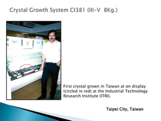
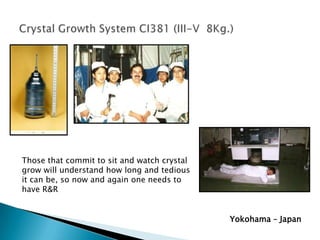
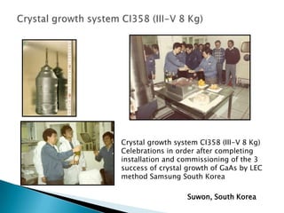
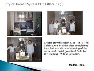
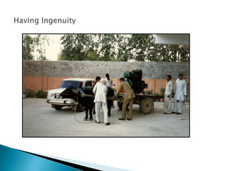
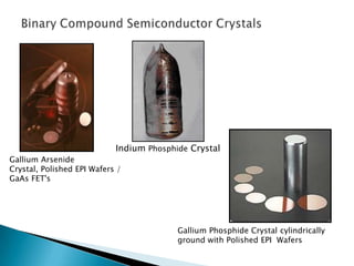
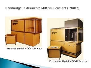
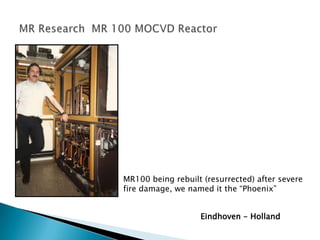
This document summarizes the author's experiences over many years working in the semiconductor crystal growth industry, traveling worldwide. It describes his first job in the industry at MR Research in Cambridge, UK. It then provides brief descriptions of some of the author's work with various crystal growth systems and MOCVD reactors in locations including England, Holland, India, Canada, Italy, France, Taiwan, Japan, and South Korea. It discusses his involvement with growing crystals such as GaAs, InP, GaP, YAG, and GGG. It also shares some of the author's observations about visiting India and interacting with people there.
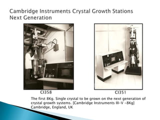
![Cambridge Instruments Crystal Growth StationsNext GenerationCI 351CI358CI351The first 8Kg. Single crystal to be grown on the next generation of crystal growth systems. [Cambridge Instruments III-V -8Kg]Cambridge, England, UK](https://image.slidesharecdn.com/crystalgrowthmocvdexperience3-12714550225517-phpapp02/85/Crystal-Growth-amp-Mocvd-Experience3-7-320.jpg)