Downloaded 109 times
![Packaging
Dual Inline Package and its lead-frame
Steps in Lead Frame Manufacture:
(1) Cut copper strips
(2) Clean in a chemical bath
(3) laminate a layer of photoresist
(4) Expose photoresist through mask
(5) Develop and etch
(6) Remove lamination
(7) Plate internal regions with gold/silver
Dual Inline Package and its lead-frame
Steps in Lead Frame Manufacture:
(1) Cut copper strips
(2) Clean in a chemical bath
(3) laminate a layer of photoresist
(4) Expose photoresist through mask
(5) Develop and etch
(6) Remove lamination
(7) Plate internal regions with gold/silver
- Make leadframe
- Die attachment (chip bonded to leadframe using epoxy)
- Wire bonding (ultrasonic welding)
- Encapsulation (moisture resistant coating)
- Molding (plastic package)
- Marking (chip number, co. name, marked on package [laser, silkscreen])
- DTFS: deflash, trim the leadframe, form the leads, singulate (cut dambars)
- Leadfinishing: electroplating the leads](https://image.slidesharecdn.com/glompses-140811130806-phpapp01/85/Molecular-Beam-Epitaxy-MBE-14-320.jpg)

![Integrated Circuit (IC) Manufacture
- Slicing the Silicon ingot
- Fabrication of IC’s (Lithography, Sputtering, diffused junction, …)
- Testing each IC on the slice
[source: www.towajapan.co.jp]
- Dicing (cutting each chip out with a diamond saw)
- Packaging](https://image.slidesharecdn.com/glompses-140811130806-phpapp01/85/Molecular-Beam-Epitaxy-MBE-16-320.jpg)


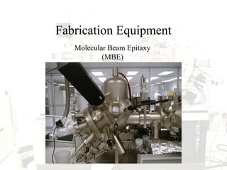
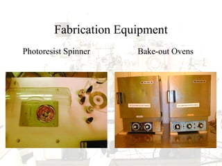
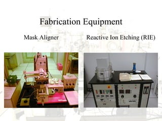
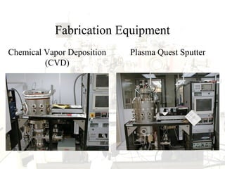
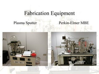
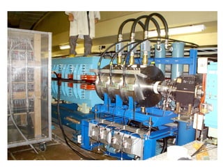
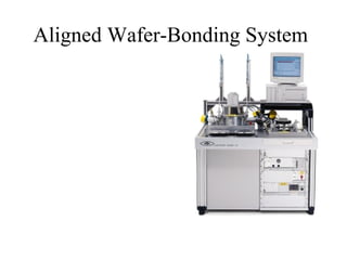
The document outlines various fabrication equipment and processes used in microelectronics, including molecular beam epitaxy, chemical vapor deposition, and reactive ion etching. It details the steps involved in manufacturing printed circuit boards and integrated circuits, emphasizing the importance of each step in ensuring quality and functionality. Additionally, references to academic lectures and textbooks are provided for further reading on the topic.


![Thin_Film_Technology_introduction[1]](https://cdn.slidesharecdn.com/ss_thumbnails/1b4496c8-2102-411b-8465-a3dd3f398327-150205034538-conversion-gate02-thumbnail.jpg?width=640&height=640&fit=bounds)


