Download to read offline
![Akshay Kumar Kansal Int. Journal of Engineering Research and Applications www.ijera.com
ISSN: 2248-9622, Vol. 5, Issue 12, (Part - 2) December 2015, pp.05-10
www.ijera.com 6|P a g e
minimum drain to source saturation voltage Vds,sat
across them. So the maximum output differential
swing can be given by the equation 2Vsupply -
10Vds,saturation - 6Vmargin [1].
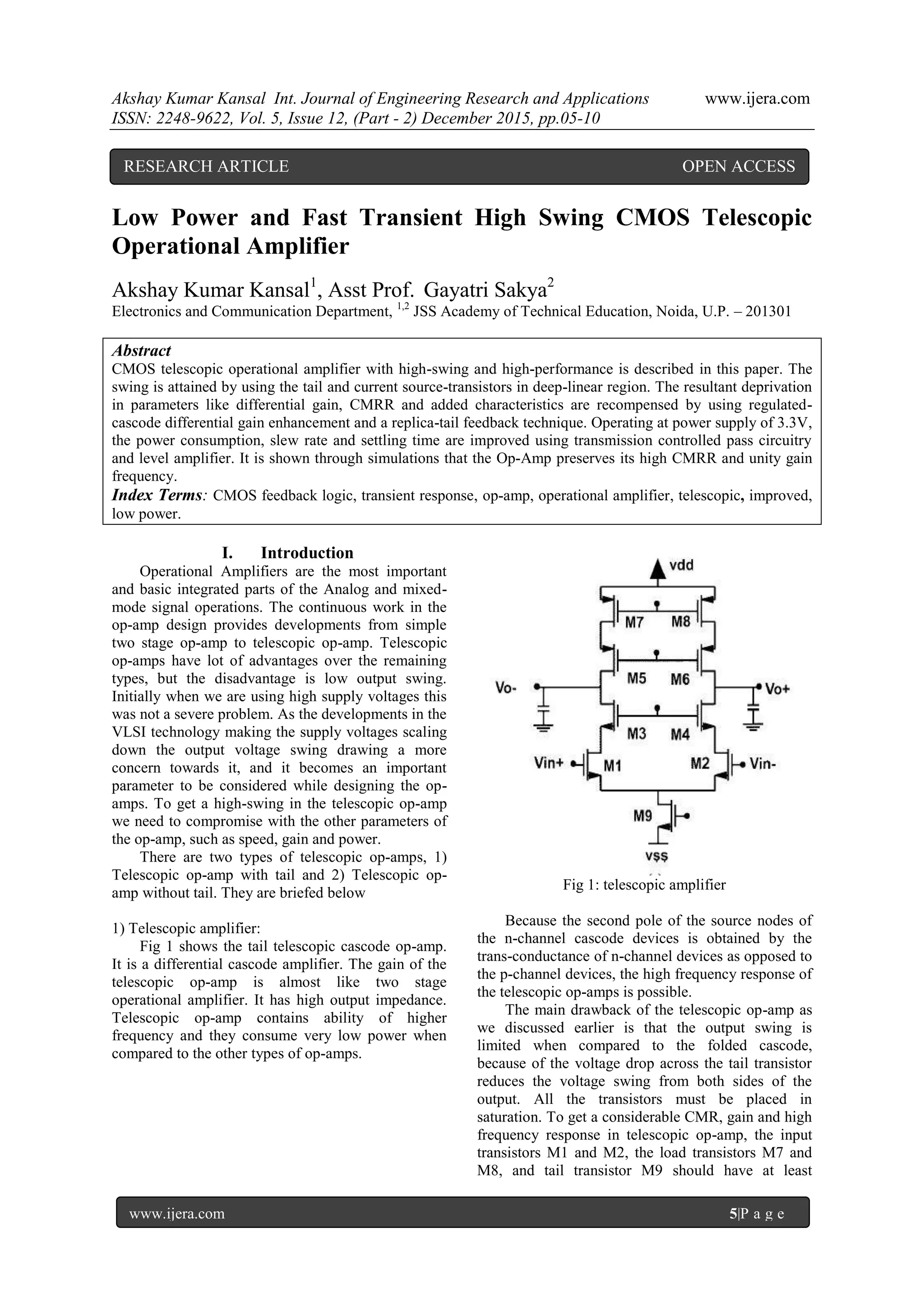
2) No-tail telescopic op-amp:
Fig 2: No-tail telescopic op-amp
No-tail telescopic op-amp is shown in above fig
2. Because there is no need of voltage drop across the
tail transistor, in the no-tail telescopic op-amp the
output voltage swing will be improved. The amount
of voltage swing improved in no-tail op-amp will be
equal to 2Vds,saturation + 2Vmargine. To get this improved
output swing in the telescopic op-amp we have to
compromise with the CMRR, PSRR of the telescopic
op-amp. In addition to that the parameters like
settling time and unity gain frequency of the
telescopic op-amp are sensitive to the input common-
mode and variations in the supply voltage.
II. High-swing Op-amp
A) why high-swing op-amps?
The relationship among the parameters of op-
amp is given by
𝑆𝑁𝑅 .(𝑠𝑝𝑒𝑒𝑑 )
𝑃
=
𝑠𝑤𝑖𝑛𝑔 2
𝛾(
𝑘𝑇
𝐶
)
.
𝛽(
𝑔𝑚
𝐶
)
𝑉 𝑠𝑢𝑝𝑝𝑙𝑦 .(𝜆𝐼)
.....(1)
Where SNR is signal to noise ratio, P is power, β is
the feedback factor of the closed loop op-amp, 𝜆 is
the ratio of total current consumption of the
operational amplifier to the current flowing through
one of the input devices, 𝛾 is the number of kT/C
noise contributions at the output of the amplifier.
kT/C is the thermal noise which is dominant in the
analog circuits.
The equation (1) can be represented in the simplified
form as
𝑆𝑁𝑅 .(𝑠𝑝𝑒𝑒𝑑 )
𝑃
𝛼
𝑠𝑤𝑖𝑛𝑔 2
𝑉 𝑠𝑢𝑝𝑝𝑙𝑦
....... (2)
From the above equation we can incur that if the
swing is high then either SNR is high or power
consumption P is low. Here the speed will be
determined by the location of the dominant pole of
the operational amplifier. So the overall performance
of the op-amp will be improved.
B. Procedure to improve the swing:
Fig 3: procedure for improving swing
If we want to improve the output swing we need
to reduce the voltage drop across the tail and the load
transistors. To reduce the voltage drop across these
transistors, we need to drive the tail transistor M9,
and load transistors M7 and M8 into deep linear
region[2]. As these transistors or operating in the
triode region the marginal voltage Vmargin need not to
be considered. The output swing equation is given by
2Vsupply - 2Vmargin - 6Vds, saturation - 2Vds,linear-tail -
2Vds,linear-load, where Vds,linear-tail is the voltage drop
across the drain and source of the tail transistor in the
linear region and Vds,linear-load is the voltage drop
across the drain to source of the load transistors in the
linear region. The swing obtained in this method is
not only superior to the telescopic op-amp but also
superior to the regular folded cascode amplifier. The
improvement in the swing is because of i. no longer
we need marginal voltage, ii. difference between
Vds,sat and the voltage across the devices in the linear
region. Any voltage reduction in across the tail
transistor M9 will improve the voltage swing by
twofold of the reduction, because the tail transistor is
connected to the both sides of the output of the op-
amp.
III. Implementation of op-amp :
Description of the circuit:](https://image.slidesharecdn.com/b512020510-151224111837/75/Low-Power-and-Fast-Transient-High-Swing-CMOS-Telescopic-Operational-Amplifier-2-2048.jpg)
![Akshay Kumar Kansal Int. Journal of Engineering Research and Applications www.ijera.com
ISSN: 2248-9622, Vol. 5, Issue 12, (Part - 2) December 2015, pp.05-10
www.ijera.com 7|P a g e
Fig 4: gain amplification across p-channel
The op-amp architecture will be determined by
the requirements in the application such as speed,
SNR, or power. The amplifier shown in fig 4 uses
standard folded-cascode amplifier architecture. The
input applied at the gate of the transistor named as
the M5E sets the drain voltage of the M7 and M8 in
the main amplifier.
The modified amplifier is shown in shown in fig
5 below
Fig 5: gain amp across n-channel
The transistors in shaded region M3X, M4X,
M7X and M8X act as active load. This amplifier
serves as replica amplifier without Vt.
This amplifier has many advantages, i) the
current through the single third input transistor will
be reused in the new differential pair and it will
reduce the additional power required to construct
amplifier, ii) the common voltage at the inputs of this
enhancement amplifier equals the common-mode
voltage of inputs of amplifier iii) ensures good
replica matching, which improves the performance of
the replica-tail feedback technique, iv) this
implementation allows simultaneous setting of the dc
levels of the common-mode voltage at the drains of
the input devices[3]
The overall implementation is shown in below
fig 6.
Fig 6: overall implementation
Capacitance Cc can be used to push the second
stage pole to a higher frequency. The ratio of the
transcondance of the duplication amplifier to the
capacitance Cc establishes the unity gain frequency of
the replica loop. The gain amps, on the other hand,
are stabilized by the arrangement of an explicit
capacitance and parasitic capacitance at the gate of
the cascoded devices. A cascode current-mirror is
used to supply the current to the replica circuitry. For
the common-mode feedback, the typical switched
capacitor circuit is used [5].
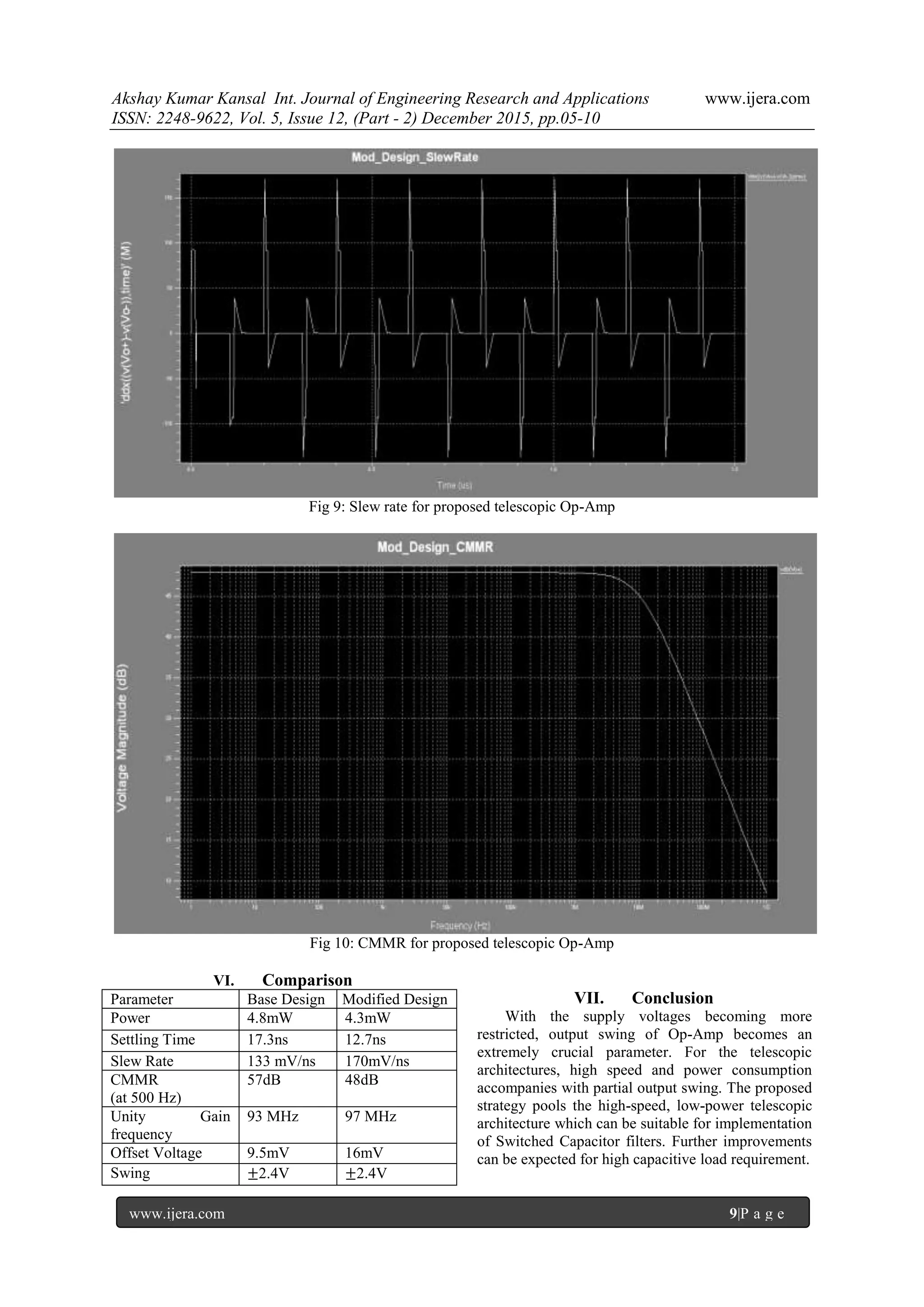
IV. Modified Circuit and Description
As we can see from the results of Base design,
the power dissipation is controlled differentially by
the input supplies only. Here in order to prevent
leakage from supply, transmission controlled
circuitry is added which helps to improvise the
previously obtained results. Also improvisation in
current flowing through tail transistor is also done by
increasing the gate voltage across the tail transistor
by employing level change amplifier, which in turn
increases the gate-to-source voltage for tail transistor.
Due to this added circuitry, settling time and slew
rate restored their base values, which were initially
degraded due to transmission controlled circuitry.
CMMR and internal gain of the amplifier remained
legitimately constant. A very small increase in output
offset voltage resulted due to very small leakages in
amplifier gain circuitry. The schematic diagram of
proposed design is shown in the fig given below. The
added circuit components transmission controller and
level change amplifier are also shown below:](https://image.slidesharecdn.com/b512020510-151224111837/75/Low-Power-and-Fast-Transient-High-Swing-CMOS-Telescopic-Operational-Amplifier-3-2048.jpg)
![Akshay Kumar Kansal Int. Journal of Engineering Research and Applications www.ijera.com
ISSN: 2248-9622, Vol. 5, Issue 12, (Part - 2) December 2015, pp.05-10
www.ijera.com 10|P a g e
References
[1] G. Nicollini, F. Moretti, and M. Conti,
“High-frequency fully differential filter
using operational amplifiers without
common-mode feedback,” IEEE J. Solid-
State Circuits, vol. 24, pp. 803–813, June
1989.
[2] P. W. Li, M. J. Chin, P. R. Gray, and R.
Castello, “A ratio-independent algorithmic
analog-to-digital conversion technique,”
IEEE J. Solid-State Circuits, vol. SC-19, pp.
1138–1143, Dec. 1984.
[3] J. N. Babanezad, “A low-output-impedance
fully differential op amp with large output
swing and continuous-time common-mode
feedback,” IEEE J. Solid-State Circuits, vol.
26, pp. 1825–1833, Dec. 1991.
[4] K. Bult and G. J. G. M. Geelen, “A fast-
settling CMOS op amp for SC circuits with
90-dB DC gain,” IEEE J. Solid-State
Circuits, vol. 25, pp. 1379–1384, Dec. 1990.
[5] J. Yang and H.-S. Lee, “A CMOS 12-bit 4
MHz pipelined A/D converter with
commutative feedback capacitor,” in Proc.
IEEE Custom Integrated Circuits Conf.,
1996, pp. 427–430.
[6] W. Krenik, J. Hellums, W.-C. Hsu, R. Nail,
and L. Izzi, “High dynamic range CMOS
amplifier design in reduced supply voltage
environment,” Tech. Dig. Midwest Symp.
Circuits and Systems, 1988, pp. 368–370.](https://image.slidesharecdn.com/b512020510-151224111837/75/Low-Power-and-Fast-Transient-High-Swing-CMOS-Telescopic-Operational-Amplifier-6-2048.jpg)

The document discusses the design and implementation of a low power, fast transient high swing CMOS telescopic operational amplifier, detailing its architecture, advantages, and trade-offs. The proposed design utilizes techniques such as regulated cascode differential gain enhancement and replica-tail feedback to improve performance metrics while maintaining a power supply of 3.3V. Simulation results indicate enhancements in settling time, slew rate, and gain, making this op-amp suitable for applications like switched capacitor filters.