Downloaded 206 times


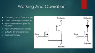


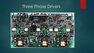

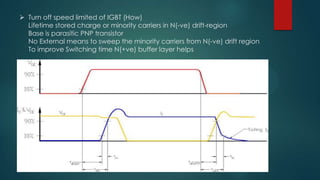


This document provides information about IGBT (Insulated Gate Bipolar Transistor) including its construction, working, applications, and advantages. It discusses that IGBT combines features of MOSFET and BJT, allowing for high current and voltage switching. IGBT has low on-state voltage drop like MOSFET and high on-state current density, making it suitable for applications requiring high switching such as power supplies, UPS, and motor drivers. The document also notes some switching characteristics of IGBT like tailing collector current and increased turn-off loss compared to MOSFET.