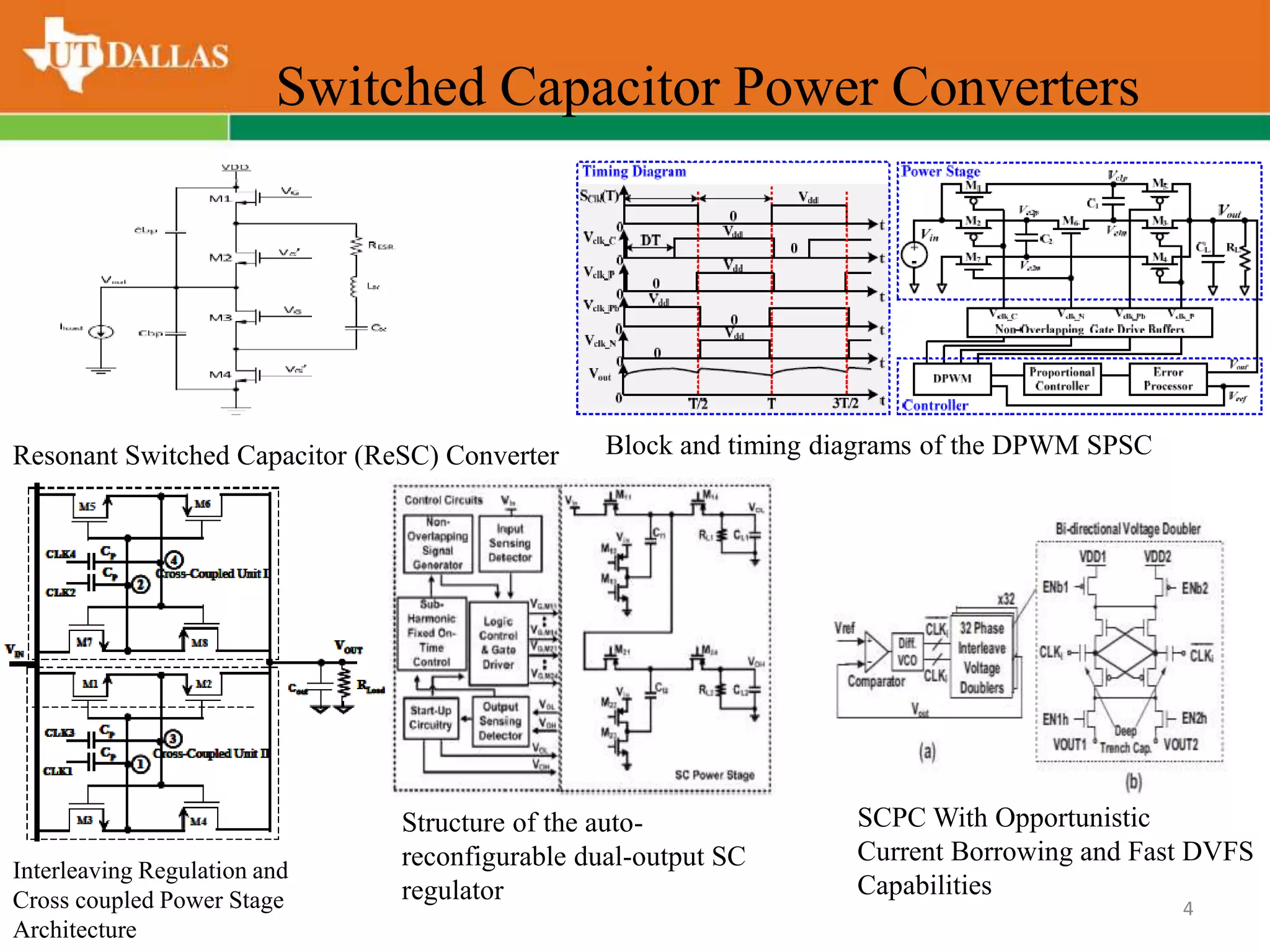
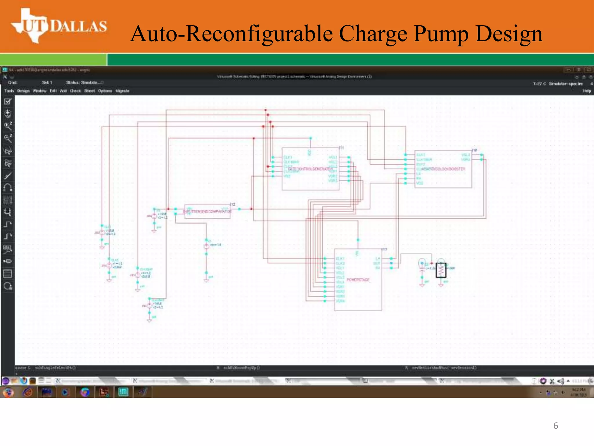
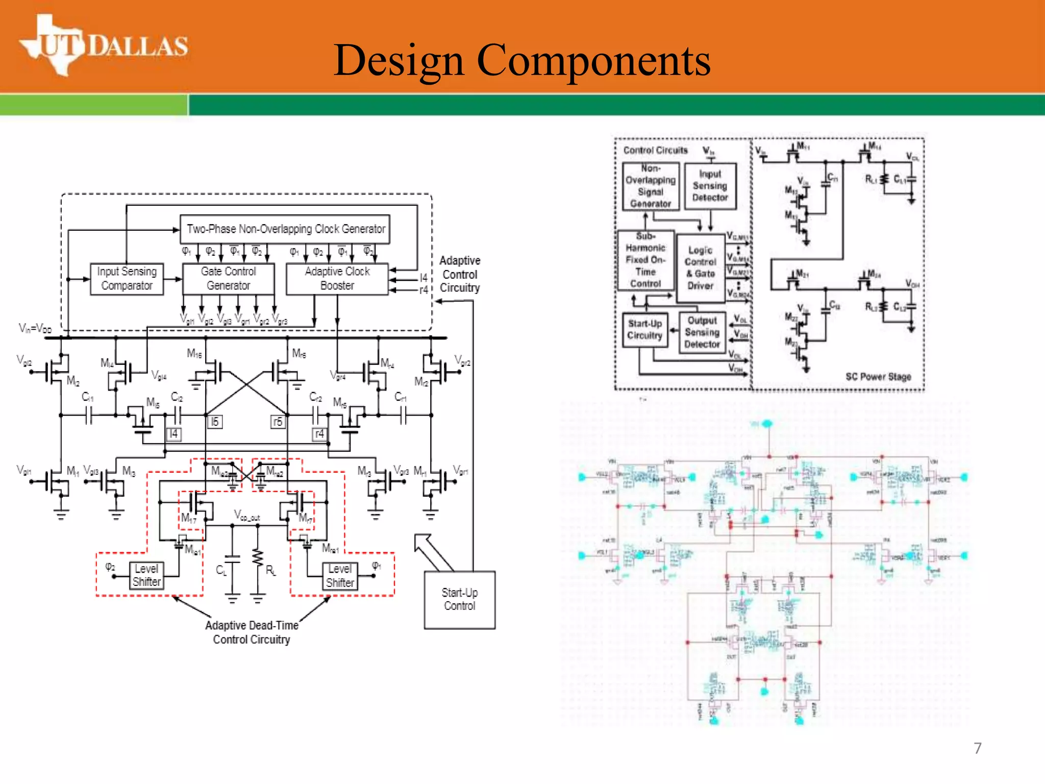
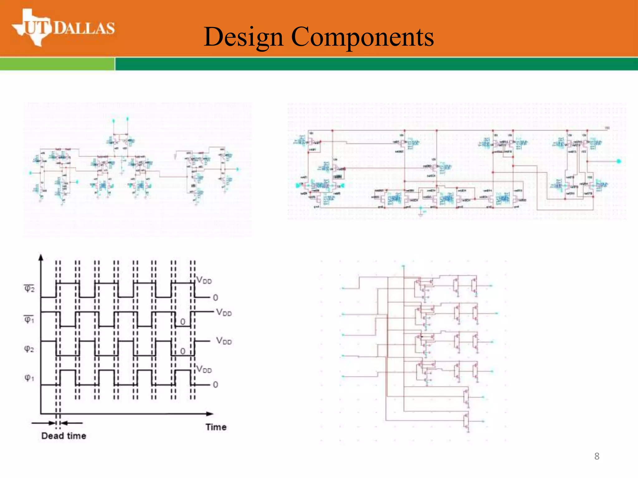
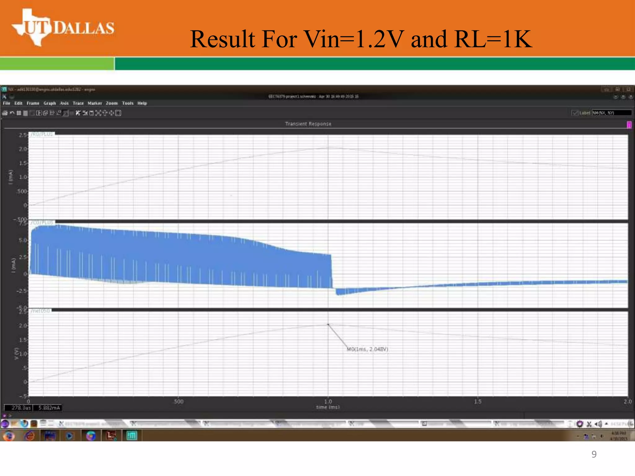
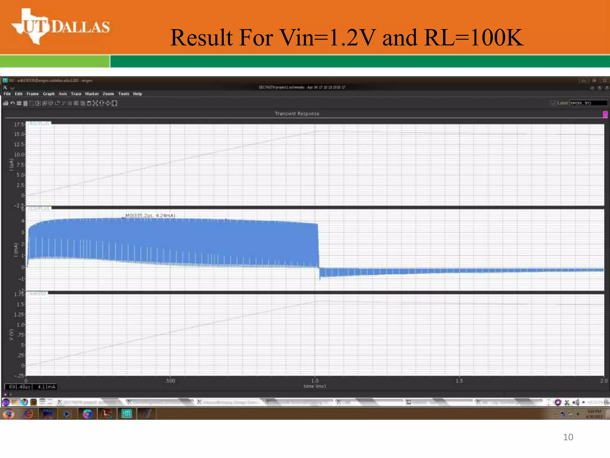
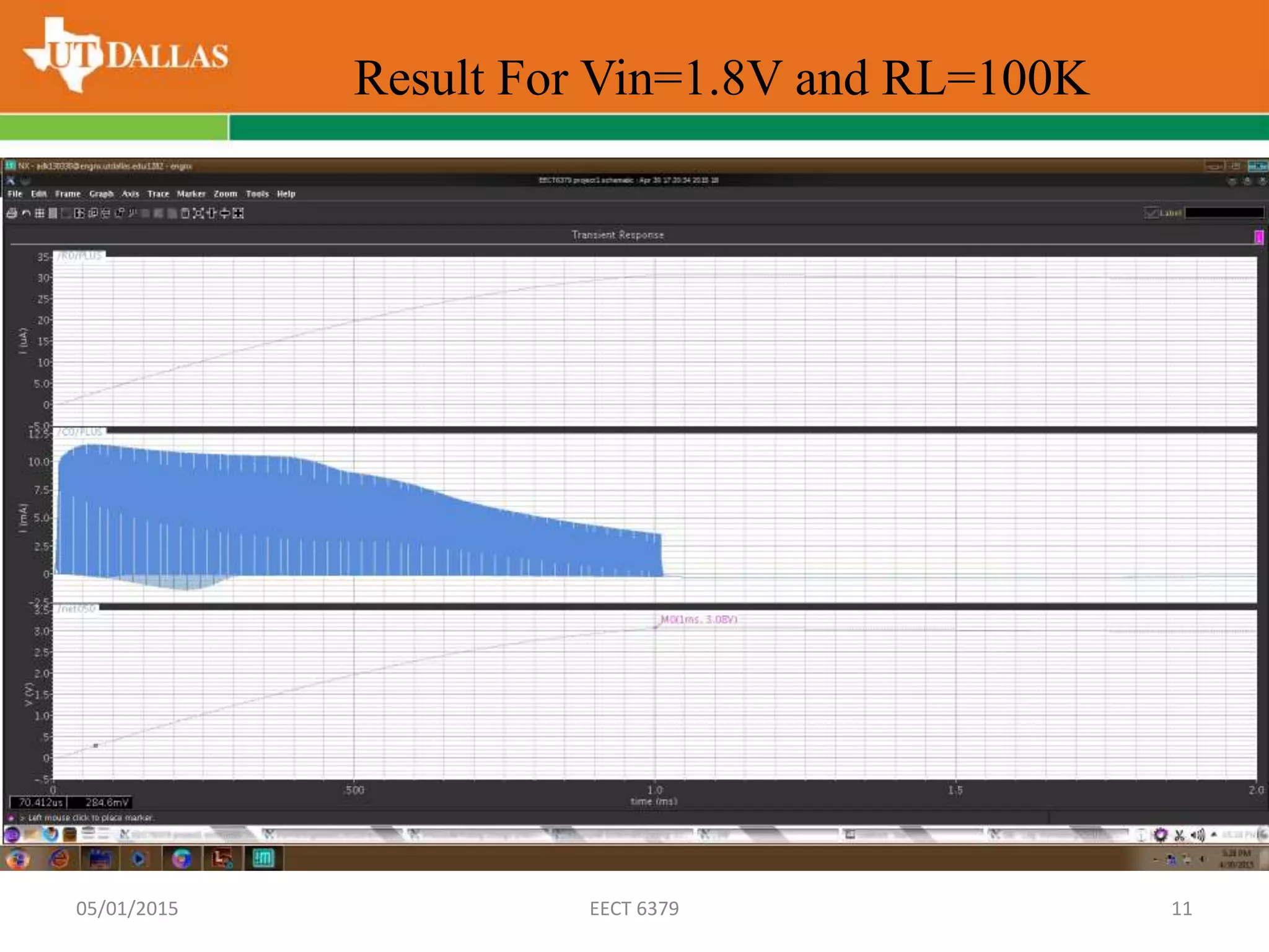
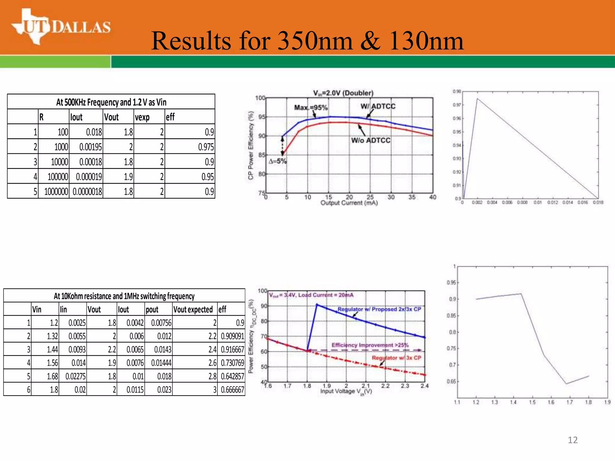
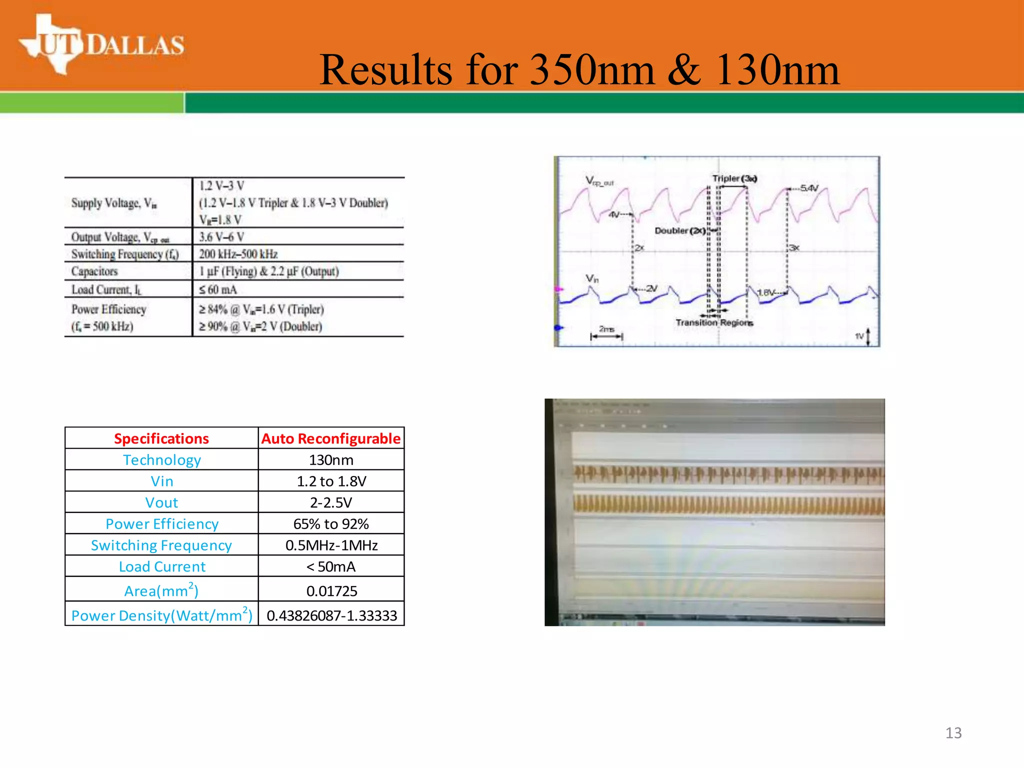
Analysis and Characterization of Different
High Density On-Chip Switched Capacitor
Power Converters in 130nm Technology
Prepared By
Aalay Kapadia (adk130330)
Nishtha Sharma (nxs135730)
05/01/2015
Team member contributions
Aalay Kapadia
Auto-Reconfigurable Switched-Capacitor DC-DC Power Converter
Nishtha Sharma
Switched-Capacitor Power Converter with Closed-Loop Interleaving Regulation
05/01/2015 2
Introduction
05/01/2015 3
•Switched capacitor is one of the DC-DC type converters.
•Similar to the SMPS, a SC converter also consists of two major components.
•Two stages are Power stage (also known as the charge pump) and a closed loop feedback controller (and/or a
feed-forward controller).
•The major benefit of SC power converters ,capability for monolithic integration at low power levels,
•Employs capacitors as energy storage devices, instead of bulky, off-chip inductors.
•One major drawback of traditional SC DC–DC converters is their ability to provide only a single Conversion
Gain (CG).
•To accommodate a large output voltage range and to be capable of powering Dynamic Voltage Frequency
Scaling (DVFS).
• Reconfigurable SC power converters using: Series-Parallel switched capacitor (SPSC) or Sequential
switched capacitor (SQSC).
• SPSC is a reconfigurable SC power converter combined with interleaving technique, which is popular
among the most of the designs.
Switched Capacitor Power Converters
4
Block and timing diagrams of the DPWM SPSCResonant Switched Capacitor (ReSC) Converter
Interleaving Regulation and
Cross coupled Power Stage
Architecture
Structure of the auto-
reconfigurable dual-output SC
regulator
SCPC With Opportunistic
Current Borrowing and Fast DVFS
Capabilities
Design focus & innovation
• Main focus -to maximize the power delivered keeping the area as low as possible for
the converter.
• Innovation in the converter is that since the capacitor sizes for the five capacitors
were decreased by a factor of almost 100 each from the original values proposed in
the paper we referred.
5
Auto-Reconfigurable Charge Pump Design
• Block level Diagram of schematic of Auto-Reconfigurable SCPC
6
7
Design Components
Design Components
8
Result For Vin=1.2V and RL=1K
9
Result For Vin=1.2V and RL=100K
10
Result For Vin=1.8V and RL=100K
05/01/2015 EECT 6379 11
Results for 350nm & 130nm
12
R Iout Vout vexp eff
1 100 0.018 1.8 2 0.9
2 1000 0.00195 2 2 0.975
3 10000 0.00018 1.8 2 0.9
4 100000 0.000019 1.9 2 0.95
5 1000000 0.0000018 1.8 2 0.9
At500KHzFrequencyand1.2VasVin
Vin Iin Vout Iout pout Voutexpected eff
1 1.2 0.0025 1.8 0.0042 0.00756 2 0.9
2 1.32 0.0055 2 0.006 0.012 2.2 0.909091
3 1.44 0.0093 2.2 0.0065 0.0143 2.4 0.916667
4 1.56 0.014 1.9 0.0076 0.01444 2.6 0.730769
5 1.68 0.02275 1.8 0.01 0.018 2.8 0.642857
6 1.8 0.02 2 0.0115 0.023 3 0.666667
At10Kohmresistanceand1MHzswitchingfrequency
13
Specifications Auto Reconfigurable
Technology 130nm
Vin 1.2 to 1.8V
Vout 2-2.5V
Power Efficiency 65% to 92%
Switching Frequency 0.5MHz-1MHz
Load Current < 50mA
Area(mm2
) 0.01725
Power Density(Watt/mm2
) 0.43826087-1.33333
Results for 350nm & 130nm
SCPC with closed loop regulation
14
Somasundaram, MN & Ma, D 2006, 'Low-ripple CMOS switched-capacitor power converter with closed-loop interleaving regulation'.
in Proceedings of the Custom Integrated Circuits Conference.
15
Gate control signals for each PMOS and NMOS power transistors are generated
internally. This avoids the need for additional clock generators and voltage
boosting circuits.
SCPC with closed loop regulation
Cross coupled power stage
16Somasundaram, MN & Ma, D 2006, 'Low-ripple CMOS switched-capacitor power converter with closed-loop interleaving regulation'.
in Proceedings of the Custom Integrated Circuits Conference.
• Nodes voltages swing between Vin and 2Vin.
• Each clock has a phase difference of 90 degrees between each other.
Output voltage & Output current
17
Output Voltage=2 V & Output current=3.081 mA
Simulations for efficiency
18
Efficiency vs Vin Vout vs Vin vs Iout
Performance summary
19
Performance summary
20
Layouts Using Cadence Virtuoso
21
Design A
Layouts Using Cadence Virtuoso
22
Design B
Q/A

Project Presentation :Analysis and characterization of different high density on chip switched capacitor power converters in 130nm technology

  • 1.
    Analysis and Characterizationof Different High Density On-Chip Switched Capacitor Power Converters in 130nm Technology Prepared By Aalay Kapadia (adk130330) Nishtha Sharma (nxs135730) 05/01/2015
  • 2.
    Team member contributions AalayKapadia Auto-Reconfigurable Switched-Capacitor DC-DC Power Converter Nishtha Sharma Switched-Capacitor Power Converter with Closed-Loop Interleaving Regulation 05/01/2015 2
  • 3.
    Introduction 05/01/2015 3 •Switched capacitoris one of the DC-DC type converters. •Similar to the SMPS, a SC converter also consists of two major components. •Two stages are Power stage (also known as the charge pump) and a closed loop feedback controller (and/or a feed-forward controller). •The major benefit of SC power converters ,capability for monolithic integration at low power levels, •Employs capacitors as energy storage devices, instead of bulky, off-chip inductors. •One major drawback of traditional SC DC–DC converters is their ability to provide only a single Conversion Gain (CG). •To accommodate a large output voltage range and to be capable of powering Dynamic Voltage Frequency Scaling (DVFS). • Reconfigurable SC power converters using: Series-Parallel switched capacitor (SPSC) or Sequential switched capacitor (SQSC). • SPSC is a reconfigurable SC power converter combined with interleaving technique, which is popular among the most of the designs.
  • 4.
    Switched Capacitor PowerConverters 4 Block and timing diagrams of the DPWM SPSCResonant Switched Capacitor (ReSC) Converter Interleaving Regulation and Cross coupled Power Stage Architecture Structure of the auto- reconfigurable dual-output SC regulator SCPC With Opportunistic Current Borrowing and Fast DVFS Capabilities
  • 5.
    Design focus &innovation • Main focus -to maximize the power delivered keeping the area as low as possible for the converter. • Innovation in the converter is that since the capacitor sizes for the five capacitors were decreased by a factor of almost 100 each from the original values proposed in the paper we referred. 5
  • 6.
    Auto-Reconfigurable Charge PumpDesign • Block level Diagram of schematic of Auto-Reconfigurable SCPC 6
  • 7.
  • 8.
  • 9.
  • 10.
    Result For Vin=1.2Vand RL=100K 10
  • 11.
    Result For Vin=1.8Vand RL=100K 05/01/2015 EECT 6379 11
  • 12.
    Results for 350nm& 130nm 12 R Iout Vout vexp eff 1 100 0.018 1.8 2 0.9 2 1000 0.00195 2 2 0.975 3 10000 0.00018 1.8 2 0.9 4 100000 0.000019 1.9 2 0.95 5 1000000 0.0000018 1.8 2 0.9 At500KHzFrequencyand1.2VasVin Vin Iin Vout Iout pout Voutexpected eff 1 1.2 0.0025 1.8 0.0042 0.00756 2 0.9 2 1.32 0.0055 2 0.006 0.012 2.2 0.909091 3 1.44 0.0093 2.2 0.0065 0.0143 2.4 0.916667 4 1.56 0.014 1.9 0.0076 0.01444 2.6 0.730769 5 1.68 0.02275 1.8 0.01 0.018 2.8 0.642857 6 1.8 0.02 2 0.0115 0.023 3 0.666667 At10Kohmresistanceand1MHzswitchingfrequency
  • 13.
    13 Specifications Auto Reconfigurable Technology130nm Vin 1.2 to 1.8V Vout 2-2.5V Power Efficiency 65% to 92% Switching Frequency 0.5MHz-1MHz Load Current < 50mA Area(mm2 ) 0.01725 Power Density(Watt/mm2 ) 0.43826087-1.33333 Results for 350nm & 130nm
  • 14.
    SCPC with closedloop regulation 14 Somasundaram, MN & Ma, D 2006, 'Low-ripple CMOS switched-capacitor power converter with closed-loop interleaving regulation'. in Proceedings of the Custom Integrated Circuits Conference.
  • 15.
    15 Gate control signalsfor each PMOS and NMOS power transistors are generated internally. This avoids the need for additional clock generators and voltage boosting circuits. SCPC with closed loop regulation
  • 16.
    Cross coupled powerstage 16Somasundaram, MN & Ma, D 2006, 'Low-ripple CMOS switched-capacitor power converter with closed-loop interleaving regulation'. in Proceedings of the Custom Integrated Circuits Conference. • Nodes voltages swing between Vin and 2Vin. • Each clock has a phase difference of 90 degrees between each other.
  • 17.
    Output voltage &Output current 17 Output Voltage=2 V & Output current=3.081 mA
  • 18.
    Simulations for efficiency 18 Efficiencyvs Vin Vout vs Vin vs Iout
  • 19.
  • 20.
  • 21.
    Layouts Using CadenceVirtuoso 21 Design A
  • 22.
    Layouts Using CadenceVirtuoso 22 Design B
  • 23.