Single Electron Transistor 
Aneesh Raveendran 
INDIA 
Aneesh Raveendran, INDIA, 
aneeshr2020@gmail.com
outline 
• What are Transistors 
• What is a SET 
• Operation of SETs 
• Application of SETs 
• How do SETs differ from Conventional 
Aneesh Raveendran, INDIA, 
aneeshr2020@gmail.com
What is a Transistor 
• A transistor is a solid state semiconductor device 
which can be used for numerous purposes including 
signal modulation, amplification, voltage 
stabilization, and many others. 
• Transistors act like a variable valve which, based on 
its input current (BJT) or input voltage (FET), allow a 
precise amount of current to flow through it from 
the circuit’s voltage supply. 
Aneesh Raveendran, INDIA, 
aneeshr2020@gmail.com
Transistor 
• Transistors 
– What are transistors? 
– How do they work? 
A transistor is a device that functions only in one direction, 
in which it draws current from its load resistor. The 
transistor is a solid state semiconductor device which can 
be used for amplification, switching, voltage stabilization, 
signal modulation and many other functions. It acts as a 
variable valve which, based on its input current (BJT) or 
input voltage (FET), allows a precise amount of current to 
flow through it from the circuit's voltage supply.
Fig 1. NPN Transistor using two diodes and connecting both anodes together
• One cathode is tied to common (the emitter); the other 
cathode (the collector) goes to a load resistor tied to the 
positive supply. For understanding, the transistor is 
configured to have the diode signal start up unimpeded until 
it reaches ~ 0.6 volts peak. At this point the base voltage will 
stop increasing. No matter how much the voltage applied 
from the generator increases (within reason), the "base" 
voltage appears to not increase. However, the current into 
that junction (two anodes) increases linearly: I = [E - 0.6]/R.
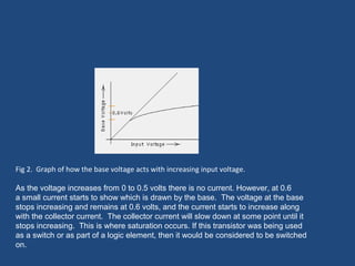
Fig 2. Graph of how the base voltage acts with increasing input voltage. 
As the voltage increases from 0 to 0.5 volts there is no current. However, at 0.6 
a small current starts to show which is drawn by the base. The voltage at the base 
stops increasing and remains at 0.6 volts, and the current starts to increase along 
with the collector current. The collector current will slow down at some point until it 
stops increasing. This is where saturation occurs. If this transistor was being used 
as a switch or as part of a logic element, then it would be considered to be switched 
on.
• Single-electron Transistor 
- what problem does it help solve? 
- what is its operation?
Problem of Making More Powerful Chips 
• Intel co-founder Gordon Moore that the number of transistors on a chip will 
approximately double every 18 to 24 months. This observation refers to what 
is known as Moore’s Law. 
• This law has given chip designers greater incentives to incorporate new 
features on silicon. 
• The chief problem facing designers comes down to size. Moore's Law works 
largely through shrinking transistors, the circuits that carry electrical signals. 
By shrinking transistors, designers can squeeze more transistors into a chip. 
However, more transistors means more electricity and heat compressed into 
an even smaller space. Furthermore, smaller chips increase performance but 
also compound the problem of complexity.
What is a SET 
• The single electron transistor is a new type of 
switching device that uses controlled electron 
tunneling to amplify current. 
• Fig 3. Single Electron Transistor 
Aneesh Raveendran, INDIA, 
aneeshr2020@gmail.com
Operation 
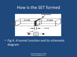
• The tunnel junction consists of two pieces of metal 
separated by a very thin (~1nm) insulator. 
• The only way for electrons in one of the metal 
electrodes to travel to the other electrode is to 
tunnel through the insulator. 
• Since tunneling is a discrete process, the electric 
charge that flows through the tunnel junction flows 
in multiples of the charge of electrons e. 
Aneesh Raveendran, INDIA, 
aneeshr2020@gmail.com
How is the SET formed 
• Fig 4. A tunnel Junction and its schematic 
diagram 
Aneesh Raveendran, INDIA, 
aneeshr2020@gmail.com
Dynamics 
• The SET is made by placing 2 tunnel junctions in 
series 
• The 2 tunnel junction create what is known as a 
ā€œCoulomb Islandā€ that electrons can only enter by 
tunneling through one of the insulators. 
• This device has 3 terminals like the FETs. 
• The cap may seem like a third tunnel junction, but is 
much thicker than the others so that no electrons 
could tunnel through it. 
• The cap simply serves as a way of setting the electric 
charge on the coulomb island. 
Aneesh Raveendran, INDIA, 
aneeshr2020@gmail.com
Procedure 
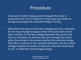
• A key point is that charge passes through the island in 
quantized units. For an electron to hop onto the island, its 
energy must equal the coulomb energy e^2/2Cg. 
• When both the gate and the bias voltages are zero, electrons 
do not have enough energy to enter the island and current 
does not flow. As the bias voltage between the source and 
drain is increased, an electron can pass through the island 
when the energy in the system reaches the coulomb energy. 
This effect is known as the coulomb blockade, and the critical 
voltage needed to transfer an electron onto the island equal 
to e/C, is called the coulomb gap energy. 
Aneesh Raveendran, INDIA, 
aneeshr2020@gmail.com
For Function 
• Capacitance of the island must be less than 
10^-17 Farads and therefore its size must be 
smaller that 10 nm. 
• The wavelength of the electrons is 
comparable with the size of the dot, which 
means that their confinement energy makes a 
significant contribution to the coulomb 
energy. 
Aneesh Raveendran, INDIA, 
aneeshr2020@gmail.com
The Coulomb Island 
Aneesh Raveendran, INDIA, 
aneeshr2020@gmail.com
Coulomb Island 
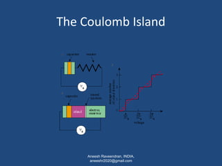
(a) When a capacitor is charged through a resistor, the 
charge on the capacitor is proportional to the 
applied voltage and shows no sign of quantization. 
(b) When a tunnel junction replaces the resistor, a 
conducting island is formed between the junction 
and the capacitor plate. In this case the average 
charge on the island increases in steps as the 
voltage is increased 
c) The steps are sharper for more resistive barriers and 
at lower temperatures. 
Aneesh Raveendran, INDIA, 
aneeshr2020@gmail.com
Coulomb Blockade 
• The effect in which electron can not pass 
through the island unless the energy in the 
system is equal to the coulomb energy 
e^2/Cg. 
• Coulomb blockade tries to alleviate any leak 
by current during the off state of the SET. 
Aneesh Raveendran, INDIA, 
aneeshr2020@gmail.com
Application of SETs 
• Quantum computers 
-1000x Faster 
• Microwave Detection 
• High Sensitivity Electrometer 
Aneesh Raveendran, INDIA, 
aneeshr2020@gmail.com
Conclusion 
• Researchers may someday assemble these 
transistors into molecular versions of silicon chips , 
but there are still formidable hurdles to cross. 
• SETs could be used for memory device, but even the 
latest SETs suffer from ā€œoffset chargesā€, which 
means that the gate voltage needed to achieve 
maximum current varies randomly from device to 
device. Such fluctuations make it impossible to build 
complex circuits. 
• The future does look bright for these devices. 
Aneesh Raveendran, INDIA, 
aneeshr2020@gmail.com
Thank you 
Aneesh Raveendran 
ā€œA common Manā€, 
INDIA 
aneeshr2020@gmail.com 
Aneesh Raveendran, INDIA, 
aneeshr2020@gmail.com

Single_Electron_Transistor_Aneesh_Raveendran

  • 1.
    Single Electron Transistor Aneesh Raveendran INDIA Aneesh Raveendran, INDIA, aneeshr2020@gmail.com
  • 2.
    outline • Whatare Transistors • What is a SET • Operation of SETs • Application of SETs • How do SETs differ from Conventional Aneesh Raveendran, INDIA, aneeshr2020@gmail.com
  • 3.
    What is aTransistor • A transistor is a solid state semiconductor device which can be used for numerous purposes including signal modulation, amplification, voltage stabilization, and many others. • Transistors act like a variable valve which, based on its input current (BJT) or input voltage (FET), allow a precise amount of current to flow through it from the circuit’s voltage supply. Aneesh Raveendran, INDIA, aneeshr2020@gmail.com
  • 4.
    Transistor • Transistors – What are transistors? – How do they work? A transistor is a device that functions only in one direction, in which it draws current from its load resistor. The transistor is a solid state semiconductor device which can be used for amplification, switching, voltage stabilization, signal modulation and many other functions. It acts as a variable valve which, based on its input current (BJT) or input voltage (FET), allows a precise amount of current to flow through it from the circuit's voltage supply.
  • 5.
    Fig 1. NPNTransistor using two diodes and connecting both anodes together
  • 6.
    • One cathodeis tied to common (the emitter); the other cathode (the collector) goes to a load resistor tied to the positive supply. For understanding, the transistor is configured to have the diode signal start up unimpeded until it reaches ~ 0.6 volts peak. At this point the base voltage will stop increasing. No matter how much the voltage applied from the generator increases (within reason), the "base" voltage appears to not increase. However, the current into that junction (two anodes) increases linearly: I = [E - 0.6]/R.
  • 7.
    Fig 2. Graphof how the base voltage acts with increasing input voltage. As the voltage increases from 0 to 0.5 volts there is no current. However, at 0.6 a small current starts to show which is drawn by the base. The voltage at the base stops increasing and remains at 0.6 volts, and the current starts to increase along with the collector current. The collector current will slow down at some point until it stops increasing. This is where saturation occurs. If this transistor was being used as a switch or as part of a logic element, then it would be considered to be switched on.
  • 8.
    • Single-electron Transistor - what problem does it help solve? - what is its operation?
  • 9.
    Problem of MakingMore Powerful Chips • Intel co-founder Gordon Moore that the number of transistors on a chip will approximately double every 18 to 24 months. This observation refers to what is known as Moore’s Law. • This law has given chip designers greater incentives to incorporate new features on silicon. • The chief problem facing designers comes down to size. Moore's Law works largely through shrinking transistors, the circuits that carry electrical signals. By shrinking transistors, designers can squeeze more transistors into a chip. However, more transistors means more electricity and heat compressed into an even smaller space. Furthermore, smaller chips increase performance but also compound the problem of complexity.
  • 10.
    What is aSET • The single electron transistor is a new type of switching device that uses controlled electron tunneling to amplify current. • Fig 3. Single Electron Transistor Aneesh Raveendran, INDIA, aneeshr2020@gmail.com
  • 11.
    Operation • Thetunnel junction consists of two pieces of metal separated by a very thin (~1nm) insulator. • The only way for electrons in one of the metal electrodes to travel to the other electrode is to tunnel through the insulator. • Since tunneling is a discrete process, the electric charge that flows through the tunnel junction flows in multiples of the charge of electrons e. Aneesh Raveendran, INDIA, aneeshr2020@gmail.com
  • 12.
    How is theSET formed • Fig 4. A tunnel Junction and its schematic diagram Aneesh Raveendran, INDIA, aneeshr2020@gmail.com
  • 13.
    Dynamics • TheSET is made by placing 2 tunnel junctions in series • The 2 tunnel junction create what is known as a ā€œCoulomb Islandā€ that electrons can only enter by tunneling through one of the insulators. • This device has 3 terminals like the FETs. • The cap may seem like a third tunnel junction, but is much thicker than the others so that no electrons could tunnel through it. • The cap simply serves as a way of setting the electric charge on the coulomb island. Aneesh Raveendran, INDIA, aneeshr2020@gmail.com
  • 14.
    Procedure • Akey point is that charge passes through the island in quantized units. For an electron to hop onto the island, its energy must equal the coulomb energy e^2/2Cg. • When both the gate and the bias voltages are zero, electrons do not have enough energy to enter the island and current does not flow. As the bias voltage between the source and drain is increased, an electron can pass through the island when the energy in the system reaches the coulomb energy. This effect is known as the coulomb blockade, and the critical voltage needed to transfer an electron onto the island equal to e/C, is called the coulomb gap energy. Aneesh Raveendran, INDIA, aneeshr2020@gmail.com
  • 15.
    For Function •Capacitance of the island must be less than 10^-17 Farads and therefore its size must be smaller that 10 nm. • The wavelength of the electrons is comparable with the size of the dot, which means that their confinement energy makes a significant contribution to the coulomb energy. Aneesh Raveendran, INDIA, aneeshr2020@gmail.com
  • 16.
    The Coulomb Island Aneesh Raveendran, INDIA, aneeshr2020@gmail.com
  • 17.
    Coulomb Island (a)When a capacitor is charged through a resistor, the charge on the capacitor is proportional to the applied voltage and shows no sign of quantization. (b) When a tunnel junction replaces the resistor, a conducting island is formed between the junction and the capacitor plate. In this case the average charge on the island increases in steps as the voltage is increased c) The steps are sharper for more resistive barriers and at lower temperatures. Aneesh Raveendran, INDIA, aneeshr2020@gmail.com
  • 18.
    Coulomb Blockade •The effect in which electron can not pass through the island unless the energy in the system is equal to the coulomb energy e^2/Cg. • Coulomb blockade tries to alleviate any leak by current during the off state of the SET. Aneesh Raveendran, INDIA, aneeshr2020@gmail.com
  • 19.
    Application of SETs • Quantum computers -1000x Faster • Microwave Detection • High Sensitivity Electrometer Aneesh Raveendran, INDIA, aneeshr2020@gmail.com
  • 20.
    Conclusion • Researchersmay someday assemble these transistors into molecular versions of silicon chips , but there are still formidable hurdles to cross. • SETs could be used for memory device, but even the latest SETs suffer from ā€œoffset chargesā€, which means that the gate voltage needed to achieve maximum current varies randomly from device to device. Such fluctuations make it impossible to build complex circuits. • The future does look bright for these devices. Aneesh Raveendran, INDIA, aneeshr2020@gmail.com
  • 21.
    Thank you AneeshRaveendran ā€œA common Manā€, INDIA aneeshr2020@gmail.com Aneesh Raveendran, INDIA, aneeshr2020@gmail.com