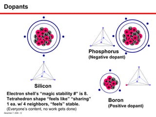
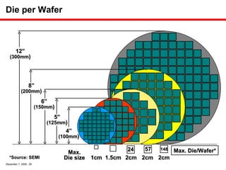
Silicon Technology Overview for Non-Engineers Bill Gascoyne
Purpose Everyone should know where their paycheck comes from “All professions are conspiracies against the laity.” George Bernard Shaw (1856-1950) Good for CFO to explain financials Good for Engineering to explain tech Practice for trainer Know your assumptions It’s fun for me!! Thanks for indulging me
Agenda Silicon, Electricity, & Transistors Chips EDA (Electronic Design Automation) Software
Silicon Silicon (Si) is a Mineral found in sand (SiO 2 ) 2nd most abundant element in Earth’s crust “Silicone” is rubber Manufacturer purchases silicon wafers Wafers sliced from ingots Ingots grown by wafer manufacturer Molten Silicon Heating Coils Silicon crystal structure
Gates Unfortunately, the word “gate” is used to mean several different things. Logic “gate” 4 transistors (1 million gates) “ Gate” terminal on a transistor (45n gate) D  Q G “ Gate” on a latch (Engineers only)
“Analog” vs. “Digital” Analog is continuous & interpolated, “real world”; Subject to interpretation, interference. Digital is numeric & discreet, information only; Hard & fast, on or off, works or doesn’t work. Phonograph is analog; the groove is shaped like the sound. CD is digital; numbers represent the sound.
More Analog vs. Digital Analog (Bipolar) transistor acts like a valve; allows so many electrons to flow at a time. Digital (CMOS) transistor is all the way  off or on,   more like a switch. “ ON” or “OFF” is less information than “How many electrons”, so digital needs more transistors for the same amount of data, but each transistor can be less precise and smaller. Analog (“Linear Region”) Digital (If smoothly turning the faucet one way made the flow increase and decrease in fits and starts, control would be non-linear.)
Current and Voltage If Electricity were Water, then: Voltage would be Pressure Current would be Volume Volume and Pressure are   Independent! Low voltage, High current High voltage, Low current Low Low High High Current Eye dropper Low Calculator Squirt gun High TV Tube Bucket Low Stereo Speakers Firehose High Oven Water Voltage Item
Electricity Current flows this way Electrons flow this way Electricity is labeled “backwards,” sort of…. Electrons are like the tiles, current is like the empty space. Which actually moves?
Basic Units Length  (meter)  (m) Time  (second)  (s) Mass  (Kilogram)  (Kg) Charge  (Coulomb)  (C) Force  (Newton)  (N)  accelerate 1Kg(1m/s)/s Pressure  (Pascal)  (Pa)  1N / 1m 2 Energy/Heat  (Joule)  (J)  1Pa/1m 3  (Nm) Power  (Watt)  (W)  J/s (or VA) Current  (Ampere)  (A)  C/s Electrical Force  (Volts)  (V)  W/A or J/C Elec. Resistance  (Ohms)  ( Ω )  V/A  (Ohm’s law: V=A  Ω ) Elec. Capacitance  (Farads)  (F)  As/V  so (F)(1/s) = 1/ Ω Elec. Inductance  (Henrys)  (H)  Vs/A  so (H)(1/s) =  Ω
Engineering Notation Each Latin number prefix = 1000X smaller milli = 10 -3 , micro = 10 -6 , nano = 10 -9 , pico = 10 -12 Small letters (m,  µ , n, p) Each Greek number prefix = 1000X larger Kilo = 10 3 , Mega = 10 6 , Giga = 10 9 , Tera = 10 12   Capital letters (K, M, G, T) Meter is to millimeter as millimeter is to micrometer
Dopants Electron shell’s “magic stability #” is 8. Tetrahedron shape “feels like” “sharing” 1 ea. w/ 4 neighbors, “feels” stable. (Everyone’s content, no work gets done) N N N + N + N + N + + N N N + N + N + N + + Silicon N N N + N + N + N + + Boron (Positive dopant) N N N + N + N + N + + N N N + N + N + N + + Phosphorus (Negative dopant)
Diode Adjacent N and P areas form a “depletion region” where they meet Opposite charges “deplete” carriers from either side, potential created “Majority carriers” are exchanged when current flows One N and one P form a diode (current flows only one way) N P +  - +  - +  - +  - +  - +  - Depletion Region
Bipolar Transistor Operation Formed by NPN or PNP diffusions with the middle (base) region very thin Base-Emitter is forward biased, remains at .7V Thin base region allows little current through the base lead Base-collector is forward-biased, but thin base allows most carriers from emitter through base to collector  Small base current multiplies collector-emitter current Emitter  Collector Base Emitter  Collector Base N P N P N P
Bipolar Cross-section When fabricated, collector and emitter are not symmetrical Operation enhanced by small emitter, lightly-doped N collector region P N- N+ N+ Collector Emitter Base
CMOS Transistor Operation We can also reverse the situation to create an N channel transistor Negative charge on gate concentrates “holes”  (+ charges) in channel (hence, P channel)  N+ N+ P- P+ P+ N- 90n
P Channel vs. N Channel n+ n+ p+ p+ P-  well N-  well N channel symbol P channel symbol n+ = heavily doped negative (P, As) N- = lightly doped negative p+ = heavily doped positive (B) P- = lightly doped positive Wafer   Source Gate Drain Oxide
Computer Logic Input Up = 1 0 Input Down = 0 1 Logic Symbol Schematic The simplest piece of computer (or “Boolean”) logic is the inverter Input “1” makes Output “0” and vice-versa. A (Input) A (Input) Z (Output) Z (Output) off on on off off on on off off on on off off on on off
More Computer Logic Adding two more transistors to the inverter results in a NAND (Not AND) gate. 0 1 1 1 1 0 1 0 1 1 0 0 Z B A A Z B A B Z “ bubble” always indicates “Not” A & B = !Z “ AND” shape 1 off off on on 0 1
AND vs. OR A and B and C A or B or C A Z C B C A B Z A Z B C C A B Z A B C A B C
Chips
An Illustration of Chip Scale Imagine that a wire on the  chip is the size of a road.  And roads are shoulder- to-shoulder for 7 levels. Then a transistor is the size of a car, and the chip covers most of Western Europe…
Moore’s Law Gordon Moore, co-founder of Intel, pointed out in a 1965 paper that the number of transistors on a chip had doubled roughly every two years, and he predicted that this would continue He was right; this had held true for almost fifty years The result has been an economic boon An unfortunate consequence of Moore’s Law is that the cost of creating each new generation (a.k.a. “node”) of technology has increased almost as fast We are rapidly approaching the point where Moore’s Law must end You can’t make a transistor smaller than an atom
Shrinking Transistors If the transistors of the Intel 4004 (10 µ ) were the size of a Humvee, a 45n transistor would be the size of a sesame seed
More about scale  A micrometer (formerly known as a micron) is one millionth of a meter. A piece of human hair is about 100 micrometers thick. The speed of light is about one foot per nanosecond (billionth of a second). There are as many nanoseconds in a second as there have been seconds since 1977. 31.7 years
Die per Wafer *Source: SEMI Max. Die size Max. Die/Wafer* 12” (300mm ) 8” (200mm ) 6” (150mm ) 5” (125mm ) 4” (100mm ) 1cm 24 2cm 57 2cm 148 2cm 1.5cm
3-D Chip Structure Several layers in the transistor Two more layers for each wire level One for wires, one for vias between wire levels Transistor Silicon substrate 1 st  level wire 2 nd  level wire 3 rd  level wire 4 th  level wire 5 th  level wire
Photolithography: What’s in a Word? Writing in Stone with Light Photo litho graphy
Each Layer is Drawn on a Mask Ultraviolet Light Source 4:1 reduction lens The wafer is coated with a light-sensitive resin  called   photoresist . It is moved by a machine  called a  stepper . The glass mask (actually called a  reticle ) is four times the size of the die.
Photolithography, Etch, Dope, Sputter Wafer (on edge) Mask Photo- resist Etch Dope Sputter
Optical Proximity Correction (OPC) In the late 80’s, it was thought that X-rays would be needed to create smaller features It is not possible to sharply focus an image smaller than the wavelength of the light used (Currently 193nm EUV) More powerful computers based on <1 µ  process made it possible to simulate optical distortions Working the problem backwards led to distorted masks that focus the desired image Mask Image
Chip Packages PQFP TQFP PGA BGA Flip Chip DIP
Where’s the chip in the package? Die Cavity Bond Fingers PGA w/ lid removed
Printed Circuit Boards Surface-Mount Through-Hole
Software EDA Tools
What does EDA do? The Electronic Design Automation industry exists primarily to answer one question: “What pattern must be drawn on each mask in order to manufacture a chip that behaves according to the customer’s specification?” Secondary questions: How to test chips after they’re made?  How to fit chip into package? How to put wires on PC boards to connect the chips together?
Electronic Design Automation (EDA) There are three basic tasks to perform Describe the idea (Build the Model) Logic Design (Synthesis) Evaluate the idea (Test the Model) Simulate and Analyze (Predicted Chip Behavior) Transfer Design Information to Manufacturing (Realize the Model) Physical Design and Testing
Levels of Abstraction EDA Tools use approximations of data from more exact tools/measurements Like Babushka dolls As chips get more complex, job gets harder, another (bigger) doll is added Measurements/simulations of silicon diffusions (10 0  T’s) SPICE transistor models (analog waveforms) (10 2  T’s) Gate level simulations (0/1 w/ rise/fall delays) (10 5  T’s) RTL (Register Transfer Level) (clock cycles) (10 8  T’s) C-Code (abstract algorithms) At each step, results less precise Precision  ≠  Accuracy
Logical Design Tools (Synthesis)
Hardware Description Languages Purpose: Make hardware design like writing software Two main HDLs in the industry Verilog Developed privately, placed into public domain Terse, “Loosely typed” Easy to use, but allows users enough rope to hang themselves Most common VHDL Developed by US DOD committee (and looks it) Verbose, “Strongly typed” Harder to use, works well or not at all (not much “rope”) Popular for library development, also common in military and Europe
Simulation  & Analysis Tools
Many Different Questions, Many Different Tasks What will it do? Simulation How fast will it go? Delay prediction Static Timing Analysis (STA) Statistical Static Timing Analysis (SSTA) How different is it from the previous version? Formal Verification How will we test it? Design For Test (DFT) Automatic Test Pattern Generation (ATPG) How well will it yield? Design For Manufacturability (DFM) Design Rule Checks (DRC)
Physical Design Tools
Physical Design Basics: Place & Route Place How best to fit everything together on the chip “Jigsaw puzzle” (but w/ abstract picture – many solutions) Route How best to connect everything once it’s placed “Traveling Salesman Problem”
Companies Companies that make chips: Intel, AMD, National, TI, Toshiba, Fujitsu “ Fabless” companies: LSI, Nvidia, MIPS, ARM, ++++ Fab-only companies (fabs for the fabless): TSMC, Chartered, UMC FPGA companies (programmable chips; fabless): Xylinx, Altera, Actel, Atmel EDA (Software) companies: Synopsys, Cadence, Mentor Graphics, Cadence, ++++ Equipment companies: Applied Materials, Ultratech Tester & measurement companies:  Credence, KLA Tencor, Teradyne, Agilent, Nanometrics
Summary Chips made from Silicon Moore’s Law: electronics keep getting better/cheaper Mfg. setup (“tooling”) is very expensive Can’t afford to be wrong EDA ensures chip will work before it’s built
Thank you!

Tech Overview

  • 1.
    Silicon Technology Overviewfor Non-Engineers Bill Gascoyne
  • 2.
    Purpose Everyone shouldknow where their paycheck comes from “All professions are conspiracies against the laity.” George Bernard Shaw (1856-1950) Good for CFO to explain financials Good for Engineering to explain tech Practice for trainer Know your assumptions It’s fun for me!! Thanks for indulging me
  • 3.
    Agenda Silicon, Electricity,& Transistors Chips EDA (Electronic Design Automation) Software
  • 4.
    Silicon Silicon (Si)is a Mineral found in sand (SiO 2 ) 2nd most abundant element in Earth’s crust “Silicone” is rubber Manufacturer purchases silicon wafers Wafers sliced from ingots Ingots grown by wafer manufacturer Molten Silicon Heating Coils Silicon crystal structure
  • 5.
    Gates Unfortunately, theword “gate” is used to mean several different things. Logic “gate” 4 transistors (1 million gates) “ Gate” terminal on a transistor (45n gate) D Q G “ Gate” on a latch (Engineers only)
  • 6.
    “Analog” vs. “Digital”Analog is continuous & interpolated, “real world”; Subject to interpretation, interference. Digital is numeric & discreet, information only; Hard & fast, on or off, works or doesn’t work. Phonograph is analog; the groove is shaped like the sound. CD is digital; numbers represent the sound.
  • 7.
    More Analog vs.Digital Analog (Bipolar) transistor acts like a valve; allows so many electrons to flow at a time. Digital (CMOS) transistor is all the way off or on, more like a switch. “ ON” or “OFF” is less information than “How many electrons”, so digital needs more transistors for the same amount of data, but each transistor can be less precise and smaller. Analog (“Linear Region”) Digital (If smoothly turning the faucet one way made the flow increase and decrease in fits and starts, control would be non-linear.)
  • 8.
    Current and VoltageIf Electricity were Water, then: Voltage would be Pressure Current would be Volume Volume and Pressure are Independent! Low voltage, High current High voltage, Low current Low Low High High Current Eye dropper Low Calculator Squirt gun High TV Tube Bucket Low Stereo Speakers Firehose High Oven Water Voltage Item
  • 9.
    Electricity Current flowsthis way Electrons flow this way Electricity is labeled “backwards,” sort of…. Electrons are like the tiles, current is like the empty space. Which actually moves?
  • 10.
    Basic Units Length (meter) (m) Time (second) (s) Mass (Kilogram) (Kg) Charge (Coulomb) (C) Force (Newton) (N) accelerate 1Kg(1m/s)/s Pressure (Pascal) (Pa) 1N / 1m 2 Energy/Heat (Joule) (J) 1Pa/1m 3 (Nm) Power (Watt) (W) J/s (or VA) Current (Ampere) (A) C/s Electrical Force (Volts) (V) W/A or J/C Elec. Resistance (Ohms) ( Ω ) V/A (Ohm’s law: V=A Ω ) Elec. Capacitance (Farads) (F) As/V so (F)(1/s) = 1/ Ω Elec. Inductance (Henrys) (H) Vs/A so (H)(1/s) = Ω
  • 11.
    Engineering Notation EachLatin number prefix = 1000X smaller milli = 10 -3 , micro = 10 -6 , nano = 10 -9 , pico = 10 -12 Small letters (m, µ , n, p) Each Greek number prefix = 1000X larger Kilo = 10 3 , Mega = 10 6 , Giga = 10 9 , Tera = 10 12 Capital letters (K, M, G, T) Meter is to millimeter as millimeter is to micrometer
  • 12.
    Dopants Electron shell’s“magic stability #” is 8. Tetrahedron shape “feels like” “sharing” 1 ea. w/ 4 neighbors, “feels” stable. (Everyone’s content, no work gets done) N N N + N + N + N + + N N N + N + N + N + + Silicon N N N + N + N + N + + Boron (Positive dopant) N N N + N + N + N + + N N N + N + N + N + + Phosphorus (Negative dopant)
  • 13.
    Diode Adjacent Nand P areas form a “depletion region” where they meet Opposite charges “deplete” carriers from either side, potential created “Majority carriers” are exchanged when current flows One N and one P form a diode (current flows only one way) N P + - + - + - + - + - + - Depletion Region
  • 14.
    Bipolar Transistor OperationFormed by NPN or PNP diffusions with the middle (base) region very thin Base-Emitter is forward biased, remains at .7V Thin base region allows little current through the base lead Base-collector is forward-biased, but thin base allows most carriers from emitter through base to collector Small base current multiplies collector-emitter current Emitter Collector Base Emitter Collector Base N P N P N P
  • 15.
    Bipolar Cross-section Whenfabricated, collector and emitter are not symmetrical Operation enhanced by small emitter, lightly-doped N collector region P N- N+ N+ Collector Emitter Base
  • 16.
    CMOS Transistor OperationWe can also reverse the situation to create an N channel transistor Negative charge on gate concentrates “holes” (+ charges) in channel (hence, P channel) N+ N+ P- P+ P+ N- 90n
  • 17.
    P Channel vs.N Channel n+ n+ p+ p+ P- well N- well N channel symbol P channel symbol n+ = heavily doped negative (P, As) N- = lightly doped negative p+ = heavily doped positive (B) P- = lightly doped positive Wafer Source Gate Drain Oxide
  • 18.
    Computer Logic InputUp = 1 0 Input Down = 0 1 Logic Symbol Schematic The simplest piece of computer (or “Boolean”) logic is the inverter Input “1” makes Output “0” and vice-versa. A (Input) A (Input) Z (Output) Z (Output) off on on off off on on off off on on off off on on off
  • 19.
    More Computer LogicAdding two more transistors to the inverter results in a NAND (Not AND) gate. 0 1 1 1 1 0 1 0 1 1 0 0 Z B A A Z B A B Z “ bubble” always indicates “Not” A & B = !Z “ AND” shape 1 off off on on 0 1
  • 20.
    AND vs. ORA and B and C A or B or C A Z C B C A B Z A Z B C C A B Z A B C A B C
  • 21.
  • 22.
    An Illustration ofChip Scale Imagine that a wire on the chip is the size of a road. And roads are shoulder- to-shoulder for 7 levels. Then a transistor is the size of a car, and the chip covers most of Western Europe…
  • 23.
    Moore’s Law GordonMoore, co-founder of Intel, pointed out in a 1965 paper that the number of transistors on a chip had doubled roughly every two years, and he predicted that this would continue He was right; this had held true for almost fifty years The result has been an economic boon An unfortunate consequence of Moore’s Law is that the cost of creating each new generation (a.k.a. “node”) of technology has increased almost as fast We are rapidly approaching the point where Moore’s Law must end You can’t make a transistor smaller than an atom
  • 24.
    Shrinking Transistors Ifthe transistors of the Intel 4004 (10 µ ) were the size of a Humvee, a 45n transistor would be the size of a sesame seed
  • 25.
    More about scale A micrometer (formerly known as a micron) is one millionth of a meter. A piece of human hair is about 100 micrometers thick. The speed of light is about one foot per nanosecond (billionth of a second). There are as many nanoseconds in a second as there have been seconds since 1977. 31.7 years
  • 26.
    Die per Wafer*Source: SEMI Max. Die size Max. Die/Wafer* 12” (300mm ) 8” (200mm ) 6” (150mm ) 5” (125mm ) 4” (100mm ) 1cm 24 2cm 57 2cm 148 2cm 1.5cm
  • 27.
    3-D Chip StructureSeveral layers in the transistor Two more layers for each wire level One for wires, one for vias between wire levels Transistor Silicon substrate 1 st level wire 2 nd level wire 3 rd level wire 4 th level wire 5 th level wire
  • 28.
    Photolithography: What’s ina Word? Writing in Stone with Light Photo litho graphy
  • 29.
    Each Layer isDrawn on a Mask Ultraviolet Light Source 4:1 reduction lens The wafer is coated with a light-sensitive resin called photoresist . It is moved by a machine called a stepper . The glass mask (actually called a reticle ) is four times the size of the die.
  • 30.
    Photolithography, Etch, Dope,Sputter Wafer (on edge) Mask Photo- resist Etch Dope Sputter
  • 31.
    Optical Proximity Correction(OPC) In the late 80’s, it was thought that X-rays would be needed to create smaller features It is not possible to sharply focus an image smaller than the wavelength of the light used (Currently 193nm EUV) More powerful computers based on <1 µ process made it possible to simulate optical distortions Working the problem backwards led to distorted masks that focus the desired image Mask Image
  • 32.
    Chip Packages PQFPTQFP PGA BGA Flip Chip DIP
  • 33.
    Where’s the chipin the package? Die Cavity Bond Fingers PGA w/ lid removed
  • 34.
    Printed Circuit BoardsSurface-Mount Through-Hole
  • 35.
  • 36.
    What does EDAdo? The Electronic Design Automation industry exists primarily to answer one question: “What pattern must be drawn on each mask in order to manufacture a chip that behaves according to the customer’s specification?” Secondary questions: How to test chips after they’re made? How to fit chip into package? How to put wires on PC boards to connect the chips together?
  • 37.
    Electronic Design Automation(EDA) There are three basic tasks to perform Describe the idea (Build the Model) Logic Design (Synthesis) Evaluate the idea (Test the Model) Simulate and Analyze (Predicted Chip Behavior) Transfer Design Information to Manufacturing (Realize the Model) Physical Design and Testing
  • 38.
    Levels of AbstractionEDA Tools use approximations of data from more exact tools/measurements Like Babushka dolls As chips get more complex, job gets harder, another (bigger) doll is added Measurements/simulations of silicon diffusions (10 0 T’s) SPICE transistor models (analog waveforms) (10 2 T’s) Gate level simulations (0/1 w/ rise/fall delays) (10 5 T’s) RTL (Register Transfer Level) (clock cycles) (10 8 T’s) C-Code (abstract algorithms) At each step, results less precise Precision ≠ Accuracy
  • 39.
  • 40.
    Hardware Description LanguagesPurpose: Make hardware design like writing software Two main HDLs in the industry Verilog Developed privately, placed into public domain Terse, “Loosely typed” Easy to use, but allows users enough rope to hang themselves Most common VHDL Developed by US DOD committee (and looks it) Verbose, “Strongly typed” Harder to use, works well or not at all (not much “rope”) Popular for library development, also common in military and Europe
  • 41.
    Simulation &Analysis Tools
  • 42.
    Many Different Questions,Many Different Tasks What will it do? Simulation How fast will it go? Delay prediction Static Timing Analysis (STA) Statistical Static Timing Analysis (SSTA) How different is it from the previous version? Formal Verification How will we test it? Design For Test (DFT) Automatic Test Pattern Generation (ATPG) How well will it yield? Design For Manufacturability (DFM) Design Rule Checks (DRC)
  • 43.
  • 44.
    Physical Design Basics:Place & Route Place How best to fit everything together on the chip “Jigsaw puzzle” (but w/ abstract picture – many solutions) Route How best to connect everything once it’s placed “Traveling Salesman Problem”
  • 45.
    Companies Companies thatmake chips: Intel, AMD, National, TI, Toshiba, Fujitsu “ Fabless” companies: LSI, Nvidia, MIPS, ARM, ++++ Fab-only companies (fabs for the fabless): TSMC, Chartered, UMC FPGA companies (programmable chips; fabless): Xylinx, Altera, Actel, Atmel EDA (Software) companies: Synopsys, Cadence, Mentor Graphics, Cadence, ++++ Equipment companies: Applied Materials, Ultratech Tester & measurement companies: Credence, KLA Tencor, Teradyne, Agilent, Nanometrics
  • 46.
    Summary Chips madefrom Silicon Moore’s Law: electronics keep getting better/cheaper Mfg. setup (“tooling”) is very expensive Can’t afford to be wrong EDA ensures chip will work before it’s built
  • 47.