Graphene transistors and two-dimensional electronics
•
15 likes•4,094 views

This document discusses using graphene for electronic devices. It describes how graphene's zero bandgap is problematic for digital electronics but its high mobility makes it promising. Several approaches are presented to induce a bandgap, including using graphene nanoribbons, applying a vertical electric field to bilayer graphene, and creating lateral heterostructures with materials of different bandgaps. Modeling shows these approaches can effectively control the band structure and enable transistor operation. Challenges remain in fabricating devices with sufficient reproducibility and without degrading carrier mobility. Lateral heterostructure FETs are identified as one of the most promising device concepts.
![Giuseppe Iannaccone University of PisaGiuseppe Iannaccone University of Pisa2
Graphene as a material for electronicsGraphene as a material for electronics
• High mobility at room
temperature (>104
cm2
/Vs)
• Symmetric properties for
electrons and holes
• One-atom thin -> promising
for scaling
• Cheap and CMOS compatible
….but ….
… the zero energy gap is a
showstopper for use in
(digital) electronics ….
Graphene Band Structure
[nanodevice.fmns.rug.nl]](data:image/gif;base64,R0lGODlhAQABAIAAAAAAAP///yH5BAEAAAAALAAAAAABAAEAAAIBRAA7)
Recommended
More Related Content
What's hot
What's hot (20)
Similar to Graphene transistors and two-dimensional electronics
Similar to Graphene transistors and two-dimensional electronics (20)
Recently uploaded
Recently uploaded (20)
Graphene transistors and two-dimensional electronics
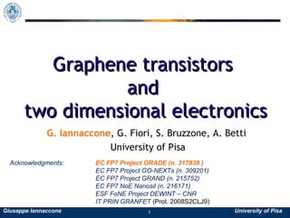
- 1. Giuseppe Iannaccone University of PisaGiuseppe Iannaccone University of Pisa1 Graphene transistorsGraphene transistors andand two dimensional electronicstwo dimensional electronics G. Iannaccone, G. Fiori, S. Bruzzone, A. Betti University of Pisa Acknowledgments: EC FP7 Project GRADE (n. 317839 ) EC FP7 Project GO-NEXTs (n. 309201) EC FP7 Project GRAND (n. 215752) EC FP7 NoE Nanosil (n. 216171) ESF FoNE Project DEWINT – CNR IT PRIN GRANFET (Prot. 2008S2CLJ9)
- 2. Giuseppe Iannaccone University of PisaGiuseppe Iannaccone University of Pisa2 Graphene as a material for electronicsGraphene as a material for electronics • High mobility at room temperature (>104 cm2 /Vs) • Symmetric properties for electrons and holes • One-atom thin -> promising for scaling • Cheap and CMOS compatible ….but …. … the zero energy gap is a showstopper for use in (digital) electronics …. Graphene Band Structure [nanodevice.fmns.rug.nl]
- 3. Giuseppe Iannaccone University of Pisa ules of graphene nanoelectronics research Increase gap, fabricate device, but keep mobility high, keep reproducibility high3
- 4. Giuseppe Iannaccone University of PisaGiuseppe Iannaccone University of Pisa4 Energy gap and the Off stateEnergy gap and the Off state Small energy gap enables leakage via interband tunneling current => high Ioff EFS EFD source channel drain Poor off state
- 5. Giuseppe Iannaccone University of PisaGiuseppe Iannaccone University of Pisa5 Energy gap and the Off stateEnergy gap and the Off state Several options to induce a bandgap have been pursued manufacturability challenges Small energy gap enables interband leakage => high Ioff EFS EFD source channel drain EFS EFD source channel drain Poor off state Good off state
- 6. Giuseppe Iannaccone University of Pisa Graphene NanoRibbons 6
- 7. Giuseppe Iannaccone University of PisaGiuseppe Iannaccone University of Pisa7 Impressive GNR ExperimentsImpressive GNR Experiments X. Li et al., Science 319, 1229 (2008) X. Li et al. PRL 100, 206803 (2008)
- 8. Giuseppe Iannaccone University of PisaGiuseppe Iannaccone University of Pisa8 Device modeling tool: NanoTCAD VIDESDevice modeling tool: NanoTCAD VIDES 3D Non-Equilibrium Green’s Functions (NEGF) solver Fully coherent transport Generic 3D structures • CNT and GNR FETs (TB atomistic) • Bilayer graphene FETs (TB atomistic) • Semiconductor NW Transistors (EMA + TB atomistic) • hBCN New version of the code as a python module – all documentation and code at: http://vides.nanotcad.com and on the nanohub.org
- 9. Giuseppe Iannaccone University of PisaGiuseppe Iannaccone University of Pisa9 Energy gap of graphene nanoribbonsEnergy gap of graphene nanoribbons Nanoribbons always have a semiconducting gap Huge gap variations for a single-dimer width change Y.-W. Son et al. PRL 97, 216803 (2006) (16,0) (14,0) (12,0)
- 10. Giuseppe Iannaccone University of Pisa DGFET with L = 15 nm, tox = 2 nm (12,0) has a width of 1.37 nm G. Fiori et al., IEEE-EDL 28, 760 (2007) Giuseppe Iannaccone University of Pisa10 GNR-FETs transfer characteristicsGNR-FETs transfer characteristics (12,0) (12,0) (14,0) (14,0) (16,0) (16,0) (16,0) with edge roughness
- 11. Giuseppe Iannaccone University of Pisa GNR intrinsic low-field mobility Full band modeling (e- and ph): A. Betti et al. IEDM 2010, APL 2011 Intrinsic mobility of 1nm GNR ~ 800 cm2 /Vs, mainly due to AC phonons. ≈10 x smaller μinα1/n2D in graphene
- 12. Giuseppe Iannaccone University of Pisa Option 2: Bilayer graphene 12
- 13. Giuseppe Iannaccone University of PisaGiuseppe Iannaccone University of Pisa13 A vertical electric field can open a gap in bilayer graphene • E.McCann, V.I.Fal'ko, PRL. 96, 086805 (2006) • E. McCann, PRB74, 161403(R) (2006) • J.B. Oostinga et al., Nat. Mat. 7, 151 (2008) • E. V. Castro et al., PRL, 99, 216802 (2007). • T. Ohta et al. Science 313, 951 (2008). Bilayer GrapheneBilayer Graphene
- 14. Giuseppe Iannaccone University of Pisa Bilayer Graphene Tunnel FET G. Fiori, G. Iannaccone EDL, Nov. 200914
- 15. TFET principle of operation
- 16. Giuseppe Iannaccone University of Pisa Tunnel Bilayer graphene FET (III)Tunnel Bilayer graphene FET (III) Transfer characteristics as a function of gate overlap
- 18. Giuseppe Iannaccone University of Pisa Atomic layers of hBN and graphene domains L. Ci et al.(Rice) Nat. Mat. 9, 430 (2010) Absorption rate of BN 5.68 eV Egap 18
- 19. Giuseppe Iannaccone University of PisaGiuseppe Iannaccone University of Pisa19 Energy gap and the Off stateEnergy gap and the Off state With a high gap region in the channel => low Ioff EFS EFD source channel drain EFS EFD source channel drain Poor off state Good off state
- 20. Giuseppe Iannaccone University of Pisa Lateral heterostructure FET 20 G. Fiori, G. Iannaccone, IEDM 2011, ACS Nano 2012
- 21. Giuseppe Iannaccone University of Pisa hBCN Bandstructure (from DFT) 21
- 22. Giuseppe Iannaccone University of Pisa LDOS: graphene FET vs BC2N FET 22
- 23. Giuseppe Iannaccone University of Pisa ID-VGS for different barrier material and length 23 BC2N tB = 5 nm
- 24. Giuseppe Iannaccone University of Pisa Graphene LHFET - Comparison with ITRS 2012 Ioff fixed at 100 nA/µm (as for HP) [Low OP has Ioff 5 nA/µm] 24
- 25. Giuseppe Iannaccone University of Pisa Advantages of LH FETs 1. Robust with respect to fabrication tolerances (self aligned gate) 2. Exploit high mobility graphene for local interconnects an S/D extensions 3. Several unexplored options for the high gap region 25
- 26. Giuseppe Iannaccone University of Pisa Lateral G-BN Heterostructures 26 M.P. Levendorf Nature 2012 (Cornell)
- 27. Giuseppe Iannaccone University of Pisa27 L. Britnell et al., Science v. 335, p. 947, 2011 Britnell et al. Nano Letters 2011 Britnell et al. Science 2011
- 28. Giuseppe Iannaccone University of Pisa Graphene-base hot electron transistor 28 S. Vaziri et al. (KTH,U. Siegen, IHP) Nano Letters 2012
- 29. Giuseppe Iannaccone University of Pisa Graphene Barristor 29 K. Yang, Science 2012 (SAIT,Columbia U., Samsung)
- 30. Giuseppe Iannaccone University of Pisa
- 31. Giuseppe Iannaccone University of Pisa Transfer characteristics 1 layer not enough 3-5 layers ON: thermionic OFF: tunnel
- 32. Giuseppe Iannaccone University of Pisa Gate on lead: poor HF performance
- 33. Giuseppe Iannaccone University of Pisa How about analog? fT gold rush Jan. 09 fT=26 GHz Apr. 09 fT=50 GHz Feb. 10 fT=100 GHz May 10 fT=100 GHz Apr. 11 fT=150 GHz
- 34. Giuseppe Iannaccone University of Pisa fT gold rush
- 35. Giuseppe Iannaccone University of Pisa Exploring the design space Extraction of series resistance Y. Wu et al., Nature, 472 p. 74, 2011 G. Fiori et al., IEDM 2012
- 36. Giuseppe Iannaccone University of Pisa Bilayer Graphene improves performance Optimized structure with tox = 4 nm , tb = 20 nm
- 37. Giuseppe Iannaccone University of Pisa Backgate voltage controls Av0
- 38. Giuseppe Iannaccone University of Pisa fT, fMAX comparable for BGFETs and Si, III-V FETs be presented at IEDM 2012
- 39. Giuseppe Iannaccone University of Pisa Graphene in microelectronics: no easy solution Nanoribbons require prohibitive fabrication tolerances and are prone to mobility degradation Bilayer graphene could be interesting: Digital: only TFETs (experiment under way) Analog: FET (focus of the GRADE project: main challenge is reducing contact resistance) Lateral Heterostructure FET (IMHO) The Most Promising device: Experiments ongoing Vertical Heterostructure FET Low on/off ratio, low fT Attempts to increase fT within GRADE (GBTs) 39
- 40. Giuseppe Iannaccone University of PisaGiuseppe Iannaccone University of Pisa Thank youThank you