Rohil kumar
17M713
INDEX
 Introduction
 History
 Background
 Quantum dots
 Higher Band Gap Material
 Fabrication
 References
Introduction
 A quantum dot solar cell (QDSC ) is a solar cell design that uses
quantum dots as the absorbing photovoltaic material.
 It attempts to replace bulk materials such as silicon, copper indium
gallium selenide (CIGS) or CdTe.
 Quantum dots have bandgaps that are tunable across a wide range of
energy levels by changing the dots' size.
 In bulk materials the bandgap is fixed by the choice of material. This
property makes quantum dots attractive for multi-junction solar cells,
where a variety of materials are used to improve efficiency by
harvesting multiple portions of the solar spectrum.
History
 The idea was noted by Burnham and Duggan in 1990.
 Using quantum dots as an alternative to molecular dyes was considered
from the earliest days of DSSC research (dye-sensitized solar cell)
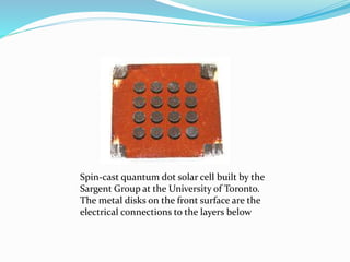
Spin-cast quantum dot solar cell built by the
Sargent Group at the University of Toronto.
The metal disks on the front surface are the
electrical connections to the layers below
Background
Solar cell concepts
 In a conventional solar cell, light is absorbed by a semiconductor,
producing an electron-hole (e-h) pair; referred to as an exciton.
 This pair is separated by an internal electric field and the resulting flow
of electrons and holes creates electric current.
 The internal electric field is created by doping one part of
semiconductor interface with atoms that act as electron donors (n-type
doping) and another with electron acceptors (p-type doping) that
results in a p-n junction.
 Generation of an e-h pair requires that the photons have energy
exceeding the bandgap of the material. Effectively, photons with
energies lower than the bandgap do not get absorbed therby reduces
current, while those that are higher can quickly thermalize to the band
edges & reduces the voltage.
 Using single material efficiency can not exceed 31%.
 31% efficiency is achieved with a bandgap of 1.3-1.4 eV ( light in infrared
spectrum). This band gap is close to that of silicon (1.1 eV), thats why
silicon dominates the market. However, silicon's efficiency is limited to
about 29%(due to fixed band gap).
 It is possible to improve on a single-junction cell by vertically stacking
cells with different bandgaps – termed a "Multi-junction" approach.
The same analysis shows that a two layer cell should have one layer
tuned to 1.64 eV and the other to 0.94 eV, providing a theoretical
performance of 44%. A three-layer cell should be tuned to 1.83, 1.16 and
0.71 eV, with an efficiency of 48%. An "infinity-layer" cell would have a
theoretical efficiency of 86%.
 Traditional (crystalline) silicon preparation methods do not lend
themselves to this approach due to lack of bandgap tunability but thin-
films of amorphous silicon can can be use to tune the bandgap.
 Most multi-junction-cell structures are based on higher performance
semiconductors, notably indium gallium arsenide (InGaAs). Three-
layer InGaAs/GaAs/InGaP cells (bandgaps 0.94/1.42/1.89 eV) hold the
efficiency record of 42.3%.
Quantum dots
 Quantum dots are semiconducting particles that have been reduced
below the size of the Exciton Bohr radius .
 Quantum dots have been referred to as "artificial atoms". These energy
levels are tuneable by changing their size, which in turn defines the
bandgap. The dots can be grown over a range of sizes, allowing them to
express a variety of bandgaps without changing the underlying
material or construction techniques.
 Bohr excitation radius for Si is little less than 5 nm, so Si nano particle
is embedded in the high band diagram dielectric material
(SiC,SiO2,Si3N4) for possible change in band gap.
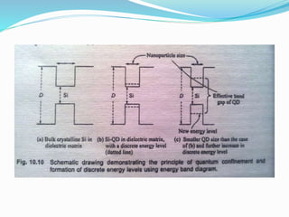
 As size of nano particle < bohr exciton radius , Ec & Ev split and move
away from each other, means effective band gap increases.
 Change in electrical and optical properties is known as Quantum
confinement of carriers. The small Si nanocrystals showing the
increased band gap due to quantum confinement are called Quantum
Dots.(QDs)
 By turning the size of Si-QDs, the band gap as high as 2.7 eV can be
obtained.
Higher Band Gap Material
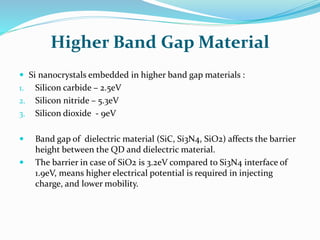
 Si nanocrystals embedded in higher band gap materials :
1. Silicon carbide – 2.5eV
2. Silicon nitride – 5.3eV
3. Silicon dioxide - 9eV
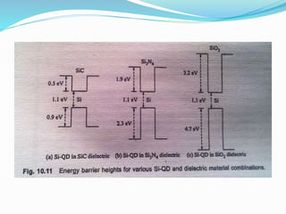
 Band gap of dielectric material (SiC, Si3N4, SiO2) affects the barrier
height between the QD and dielectric material.
 The barrier in case of SiO2 is 3.2eV compared to Si3N4 interface of
1.9eV, means higher electrical potential is required in injecting
charge, and lower mobility.
Fabrication
 Fabricated using several deposition technique:
1. PECVD (Plasma Assisted chemical vapor deposition)
2. HWCVD(Hot Wire CVD)
3. LPCVD (Low Pressure CVD )
 Requirement : uniform size of distribution, high density of Si-QD
deposition.
 Deposition of Si-rich dielectric layer followed by high temp
annealing (800 to 1100 C).
 Another approach : deposition of alternative layers of dielectric
material and Si containing layers followed by high temp annealing
crystallizes amorphous layer to Si-QDs.
 Thickness of alternative layers is in the range of few nanometers
thereby limits the growth of the QDs in the range of few nanometers
References
 Solar Photovoltaics fundamental, technologies and applications.
- Chetan Singh Solanki
 https://en.wikipedia.org/wiki/Quantum_dot
 https://en.wikipedia.org/wiki/Quantum_dot_solar_cell

Quantum dot solar cell

  • 1.
  • 2.
    INDEX  Introduction  History Background  Quantum dots  Higher Band Gap Material  Fabrication  References
  • 3.
    Introduction  A quantumdot solar cell (QDSC ) is a solar cell design that uses quantum dots as the absorbing photovoltaic material.  It attempts to replace bulk materials such as silicon, copper indium gallium selenide (CIGS) or CdTe.  Quantum dots have bandgaps that are tunable across a wide range of energy levels by changing the dots' size.  In bulk materials the bandgap is fixed by the choice of material. This property makes quantum dots attractive for multi-junction solar cells, where a variety of materials are used to improve efficiency by harvesting multiple portions of the solar spectrum.
  • 4.
    History  The ideawas noted by Burnham and Duggan in 1990.  Using quantum dots as an alternative to molecular dyes was considered from the earliest days of DSSC research (dye-sensitized solar cell)
  • 5.
    Spin-cast quantum dotsolar cell built by the Sargent Group at the University of Toronto. The metal disks on the front surface are the electrical connections to the layers below
  • 6.
    Background Solar cell concepts In a conventional solar cell, light is absorbed by a semiconductor, producing an electron-hole (e-h) pair; referred to as an exciton.  This pair is separated by an internal electric field and the resulting flow of electrons and holes creates electric current.  The internal electric field is created by doping one part of semiconductor interface with atoms that act as electron donors (n-type doping) and another with electron acceptors (p-type doping) that results in a p-n junction.  Generation of an e-h pair requires that the photons have energy exceeding the bandgap of the material. Effectively, photons with energies lower than the bandgap do not get absorbed therby reduces current, while those that are higher can quickly thermalize to the band edges & reduces the voltage.  Using single material efficiency can not exceed 31%.
  • 7.
     31% efficiencyis achieved with a bandgap of 1.3-1.4 eV ( light in infrared spectrum). This band gap is close to that of silicon (1.1 eV), thats why silicon dominates the market. However, silicon's efficiency is limited to about 29%(due to fixed band gap).  It is possible to improve on a single-junction cell by vertically stacking cells with different bandgaps – termed a "Multi-junction" approach. The same analysis shows that a two layer cell should have one layer tuned to 1.64 eV and the other to 0.94 eV, providing a theoretical performance of 44%. A three-layer cell should be tuned to 1.83, 1.16 and 0.71 eV, with an efficiency of 48%. An "infinity-layer" cell would have a theoretical efficiency of 86%.  Traditional (crystalline) silicon preparation methods do not lend themselves to this approach due to lack of bandgap tunability but thin- films of amorphous silicon can can be use to tune the bandgap.  Most multi-junction-cell structures are based on higher performance semiconductors, notably indium gallium arsenide (InGaAs). Three- layer InGaAs/GaAs/InGaP cells (bandgaps 0.94/1.42/1.89 eV) hold the efficiency record of 42.3%.
  • 8.
    Quantum dots  Quantumdots are semiconducting particles that have been reduced below the size of the Exciton Bohr radius .  Quantum dots have been referred to as "artificial atoms". These energy levels are tuneable by changing their size, which in turn defines the bandgap. The dots can be grown over a range of sizes, allowing them to express a variety of bandgaps without changing the underlying material or construction techniques.  Bohr excitation radius for Si is little less than 5 nm, so Si nano particle is embedded in the high band diagram dielectric material (SiC,SiO2,Si3N4) for possible change in band gap.  As size of nano particle < bohr exciton radius , Ec & Ev split and move away from each other, means effective band gap increases.  Change in electrical and optical properties is known as Quantum confinement of carriers. The small Si nanocrystals showing the increased band gap due to quantum confinement are called Quantum Dots.(QDs)  By turning the size of Si-QDs, the band gap as high as 2.7 eV can be obtained.
  • 10.
    Higher Band GapMaterial  Si nanocrystals embedded in higher band gap materials : 1. Silicon carbide – 2.5eV 2. Silicon nitride – 5.3eV 3. Silicon dioxide - 9eV  Band gap of dielectric material (SiC, Si3N4, SiO2) affects the barrier height between the QD and dielectric material.  The barrier in case of SiO2 is 3.2eV compared to Si3N4 interface of 1.9eV, means higher electrical potential is required in injecting charge, and lower mobility.
  • 12.
    Fabrication  Fabricated usingseveral deposition technique: 1. PECVD (Plasma Assisted chemical vapor deposition) 2. HWCVD(Hot Wire CVD) 3. LPCVD (Low Pressure CVD )  Requirement : uniform size of distribution, high density of Si-QD deposition.  Deposition of Si-rich dielectric layer followed by high temp annealing (800 to 1100 C).  Another approach : deposition of alternative layers of dielectric material and Si containing layers followed by high temp annealing crystallizes amorphous layer to Si-QDs.  Thickness of alternative layers is in the range of few nanometers thereby limits the growth of the QDs in the range of few nanometers
  • 13.
    References  Solar Photovoltaicsfundamental, technologies and applications. - Chetan Singh Solanki  https://en.wikipedia.org/wiki/Quantum_dot  https://en.wikipedia.org/wiki/Quantum_dot_solar_cell