SlideShare a Scribd company logo
1 of 33
Download to read offline
1
Chap-1&2 Sequential Circuits
❖ Introduction:-
In some logic circuit, the output of a circuit changes according to presents input as well
as past input, such circuits are known as sequential circuits.
Figure. Sequential Circuit
Unlike combinational logic circuits that change state depending upon the actual signals
being applied to their inputs at that time, Sequential Logic circuits have some form of intrinsic
“Memory” built in.
The “Sequential” means that things happen in a “sequence”, one after another and
in Sequential Logic circuits, the actual clock signal determines when things will happen next.
Simple sequential logic circuits can be constructed from standard bistable circuits such as Flip-
flops, Latches and Counters and which themselves can be made by simply connecting together
universal NAND or/and NOR gates in a particular combinational way to produce the required
sequential circuit.
❖ Difference between combinational circuit and sequential circuit:-
Sr.
No.
Combinational Circuit Sequential Circuit
1 In Combinational Circuit, the output variables at all
Depends on the combination of the input variable.
In Sequential Circuit, the
output variables depends not
only on present input but also
2
depends upon the past input
2 Memory unit is not required in Combinational Circuit Memory unit is required to
store the past input variable
3 The Combinational Circuits are faster Slower than Combinational
Circuits
4 Combinational Circuits are easy to design Sequential Circuits are harder
to design
5 Parallel adder is Combinational Circuit. Serial adder is a sequential
circuit
.
❖ Flip-Flops (F/F):-
In a digital system, user requires the circuits whose output one’s set, should remain
unchanged even if the input is changed. Such device can be used to store information in the form
of binary number. The cross-coupled gates used to store binary data are known as flip-flops.
In electronics, a flip-flop or latch is a circuit that has two stable states and can be used to
store state information. A flip-flop is a bistable multivibrator. The circuit can be made to change
state by signals applied to one or more control inputs and will have one or two outputs. It is the
basic storage element in sequential logic. Flip-flops and latches are fundamental building blocks
of digital electronics systems used in computers, communications, and many other types of
systems. Flip-flops and latches are used as data storage elements. A flip-flop stores a
single bit (binary digit) of data; one of its two states represents a "one" and the other represents a
"zero". Such data storage can be used for storage of state, and such a circuit is described
as sequential logic. There are different types of flip-flops are available such as:
1) RS flip-flop using NAND gate
2) RS flip-flop using NOR gate
3) Clocked RS flip-flop
4) JK flip-flop
5) Master – Slave JK flip-flop
6) D-type flip-flop
7) T-type Flip-flop.
3
I
II
1) RS flip-flop using NAND gate:-
Figure b) Truth Table
S
Q
Q
R
Figure a) RS F/F using NAND gate
The figure a) shows the logic diagram of RS F/F using NAND gates and figure b) shows the
truth table of a RS F/F using NAND gate.
When S=0, and R=0, both the gates output goes high (1). But these cannot be allowed
because Q always has to be complemented of Q.
When S=1, and R=0, now the output of gate-II is ‘1’. This is given as input to gate –I. So,
gate-I receives both input as ‘1’, so output goes to ‘0’. Therefore, S=1, and R=0, the outputs are
Q=0 and Q=1.
When S=0, and R=1, the output of gate-I is ‘1’. This is given as input to gate-II. Thus,
gate –II gets both inputs as ‘1’ so its output is ‘0’. Therefore, outputs are Q=1 and Q=0.
When S=1, and R=1, we can’t decide the output unless we know the previous state,
Suppose, the previous state is Q=1 and Q=0. So input to gate –I are (1,0) so output goes ‘1’.
However, Q acts as a input to gate-II, so gate –II receives both inputs as (1,1), so it’s output goes
to ‘0’. Therefore, S=1, and R=1, Q=1 and Q=0 which is nothing but previous state.
2) RS flip-flop using NOR gate:-
S Q
Q
R
Figure b) Truth Table
R S Q
0 0 No Change
0 1 0
1 0 1
1 1 Invalid
Figure a) RS F/F using NOR gate
I
II
R S Q
0 0 Forbidden
0 1 0
1 0 1
1 1 No Change
4
The figure a) shows the logic diagram of RS F/F using NOR gates and figure b) shows the truth
table of a RS F/F using NOR gate.
When S=0, and R=0, we cannot go further unless we assume the previous state. Suppose,
the previous state is Q=0 and Q=1. So input to gate –I are (0,1) so output goes ‘0’. However, Q
acts as a input to gate-II, so gate –II receives both inputs as (0,0), so it’s output goes to ‘1’.
Therefore, S=0, and R=0, Q=0 and Q=1 which is nothing but previous state (No change).
When S=1, and R=0, now the output of gate-I is ‘0’. This is given as input to gate –II. So,
gate-II receives both input as ‘0’, so output goes to ‘1’. Therefore, S=1, and R=0, the outputs are
Q=0 and Q=1.
When S=0, and R=1, the output of gate-II is ‘0’. This is given as input to gate-I. Thus,
gate –I gets both inputs as ‘0’ so its output is ‘1’. Therefore, outputs are Q=1 and Q=0.
When S=1, and R=1, the output of both NOR gates are becomes low (0), therefore, this is
invalid output.
3) Clocked RS flip-flop:-
Figure b) Truth Table
Q
Q
Figure a) Clocked RS F/F using NAND gate
The problem of an RS-F/F is that, there is no restriction on how fast the input can change,
so it possible that input may vary faster than the propagation delay of F/F. Therefore, it is
required to set or reset the F/Fs in synchronize with clock. This is achieved in clocked RS F/F’s.
The above figure shows the clocked RS F/F. The inputs will be accepted when only when clock
goes high.
When Clock=1, S=0 and R=0, Here, outputs of gate A and B are high (1). So it can not
workout further unless we know the previous state. Let us assume Q=0 and Q=1. Now, inputs to
S
A
C
Clock
D
R
B
R S Q
0 0 Qn
0 1 1
1 0 0
1 1 Qn
5
gate C are 1 and Q that is (1,1). Then output of gate C is ‘0’. This is given to input D gate. So
inputs to D gate are (1,0) so output of D gate is ‘1’. Therefore, outputs are Q=0 and Q=1 , which
is nothing but previous state or No Change(Qn).
When Clock=1, S=1 and R=0, in this condition, output of gate A is ‘0’ and output of gate
B is ‘1’. The gate C receives one of it input ‘0’, so its output becomes ‘1’. This output is given to
input of D gate. So, the inputs to the D gate are (1,1). Thus, output of gate D goes ‘0’ . Therefore,
output of the clocked RS f/F becomes Q=1 and Q=0.
When Clock=1, S=0 and R=1, here output of gate A is ‘1’ and output of gate B is ‘0’.
The gate D receives one of its input as ‘0’, So its output Q goes high(1). This is given to input of
gate C . Now input to gate C are (1,1) so its output goes to zero. Therefore, output becomes Q=0
and Q=1.
When Clock=1, S=1 and R=1, in this state we can’t decide the output unless we know
the previous state. Suppose, the previous state is Q=1, Q=0. So the outputs of gate A and B are
becomes ‘0’. Therefore, inputs to gate C are (0,0), so its output becomes ‘1’ , this is given to the
gate D as an input. The inputs to gate D are (0,1), so its output becomes ‘1’. Therefore, output
becomes Q=1 and Q=0 which is nothing but previous state.
4) JK flip-flop:-
Figure. b) Truth Table
Q
Q
Figure a) J K Flip-Flop
The RS F/F has drawback that is when both inputs are high(1,1) the output is
unpredictable. To eliminate this condition and to make the flip-flop to work even if the inputs are
1,1 the RS flip flop is modified and it becomes a JK flip flop.
J
A
C
Clock
D
K
B
Clock J K Q
1 0 0 Qn
1 0 1 0
1 1 0 1
1 1 1 Toggle
6
The above figure a) shows an JK flip flop using NAND gate and figure b) shows its truth table.
In JK flip flop the output Q is fed as an additional input to gate A and Q is fed an additional
input to gate B. To analyze the working one has to always know the previous state, consider the
following cases:-
Case-1: Clk=1, J=0, K=0, Assume Q=1 and Q = 0
The gate-A receives the inputs such as J, Clk and Q i.e 0,1,0 respectively , so the
output of gate-A becomes ‘1’. The gate-B receives the inputs such as K, clk and Q i.e 0,1 and 1
respectively. The output of gate-B becomes ‘1’. The gate-C receives the input ‘1’ from gate –A
and Q=0 , so output of gate-C becomes ‘1’ (Q). This ‘1’ is given as an input to gate D, therefore,
gate D receives inputs ‘1’ from Q and ‘1’ from gate-B, so gate-D gives the output ‘0’. Hence at
the output is Q=1 and Q=0 , which is nothing but assumed state or previous state.
Case-2: Clk=1, J=0, K=1, last state Q=1 and Q = 0
The gate-A receives the inputs such as J, Clk and Q i.e 0,1,0 respectively , so the
output of gate-A becomes ‘1’. The gate-B receives the inputs such as K, clk and Q i.e 1,1 and 1
respectively. The output of gate-B becomes ‘0’. The gate-D receives the one of its input ‘0’ from
gate –B and Q=1 , so output of gate-D becomes ‘1’ (Q). This ‘1’ is given as an input to gate C,
therefore, gate C receives inputs ‘1’ from Q and ‘1’ from gate-A, so gate-C gives the output ‘0’.
Hence at the new output is Q=0 and Q=1.
Case-3: Clk=1, J=1, K=0, last state Q=0 and Q = 1
The gate-A receives the inputs such as J, Clk and Q i.e 1,1,1 respectively , so the
output of gate-A becomes ‘0’. The gate-B receives the inputs such as K, clk and Q i.e 0,1 and 0
respectively. The output of gate-B becomes ‘1’. The gate-C receives the one of its input ‘0’ from
gate –A and Q=1 , so output of gate-C becomes ‘1’ (Q). This ‘1’ is given as an input to gate D,
therefore, gate D receives inputs ‘1’ from Q and ‘1’ from gate-B, so gate-D gives the output ‘0’.
Hence at the new output is Q=1 and Q=0.
Case-4: Clk=1, J=1, K=1, last state Q=1 and Q = 0
The gate-A receives the inputs such as J, Clk and Q i.e 1,1,0 respectively , so the
output of gate-A becomes ‘1’. The gate-B receives the inputs such as K, clk and Q i.e 1,1 and 1
respectively. The output of gate-B becomes ‘0’. The gate-D receives the one of its input ‘0’ from
gate –B and Q=1 , so output of gate-D becomes ‘1’ (Q). This ‘1’ is given as an input to gate C,
therefore, gate C receives inputs ‘1’ from Q and ‘1’ from gate-A, so gate-C gives the output ‘0’.
Hence at the new output is Q=0 and Q=1.
Therefore, in JK flip flop when both inputs are “1” it’s output toggle or
complements to each other. Hence the drawback of an previous flip flops are removed.
7
❖ Race Around Condition:-
In JK flip flop, causes of an feedback connection at the input from output, one
problem is occurs. For example:- J=1, K=1, Q=0, when the clock pulse is applied, the output
becomes Q=1. This change take place after a time interval “ t” equal to the propagation delay. If
the clock pulse is still there since, J=1, K=1 and Q=1 the output will become ‘0’ i.e Q=0. Thus
for the duration of clock pulse, the output will oscillate in between 0 and 1 and at the end of cock
pulse Q may be 0 or 1. This situation is known as Race Around condition t <tp< Tclock
Tclock
This race around condtion can be avoided by making the prorogation delay less than change in
time it means that tp< t < Tclock
5) Master slave J K Flip Flop:-
Q
Q
Figure Master Slave J K Flip-Flop
The above figure shows the master slave J K flip flop. Here, J-K flip flop are
cascaded, one works as master and another works as slave. The slave follows the master always.
t
tp
J
A
C Qm E
G
Clock
Master
Clock Slave
D
K B Qm H
F
Clock
8
Dn Qn
1 1
0 0
Tn Qn
0 Qn
1 Qn
D J Q
D-Type F/F
K
Q
Clock
T J Q
T-Type F/F
K Q
Clock
While master accepting the new inputs, then at that time slave maintaining previous output as it
is. When the master has completed the accepting the input, the slave will allow the changes cause
by the master to reach the output. During this no new input are accepted by the master. So the
output Q does not change during the propagation time of clock pulse and hence the race around
difficulty is removed. When clock pulse is ‘0’ that is clock=0, so the master is disabled and
clock=1 which causes slave is enable. The IC-7473 is dual JK flip flop is available in market.
6) D-Type Flip-Flop:-
The JK flip flop is modified into D (Delay) flip flop by adding an inverter
between J and K inputs, so that K is always complement of J. If the input is high (1), then J=1,
k=0 and hence output Q=1, if D is 0 then J=0, K=1 and hence output becomes Q=0. The output
Q after the clock pulse equals the input D. The D flip flop is used to provide a delay.
7)T-Type Flip-Flop: (Toggle):-
The J K-flip flop is modified into T-type flip flop by connecting J
and K together. This F/F changes the state with each clock pulse. It acts as a toggle switch and
hence the name as T-type flips flop. When J=K=0 means T=0, then output is Qn and when
9
J=K=1 means T=1 then output is Qn. According to the truth table of J K flip flop the T-F/F is
also known as complementing flip flop.
❖ IC – 7475(D-Flip Flop):-
D1
D2
D3
D4
Clock1
Clock2
Q1
Q1
Q2
Q2
Q3
Q3
Q4
Q4
Vcc GND
Figure . Pin diagram of IC-7475
It is a TTL IC working on +5V power supply. It is a quad bistable latch. It uses MSI
technology (Medium Scale Integration Technology). It has four inputs (D-type), 8-outputs and
two clock ‘s. One clock synchronizes two flip flops. In IC positive edge trigger is used. It is also
called as transparent latch because as long s clock=1 all variations of D are passed on to the
output.
IC-7475
D-Type F/F
CLK D Qn
0 x Last
State
1 1 1
1 0 0
10
J QA J QB J QC J QD
K K K K
❖ Counters:-
One of the most famous sub systems in digital electronics is the Counter. The counter
basically constructed using flip flops. The counters count the number of clock pulses arriving at
its input. The output of the counter is binary or BCD equivalent of the number of clock pulses
appeared at its input. The counter can be used as an instrument for measurement of time.
❖ Binary Counter / Ripple Counter / Asynchronous Counter(4-Bit):
Vcc
Clock
QA QB QC QD
Figure a) 4-bit binary counter
1 2 3
CLK
4 5 6 7 8 9 10 11 12 13
QA
QB
QC
QD
Figure b) Timing diagram of ripple counter
F/F-
D
F/F-
C
F/F-
B
F/F-
A
11
Figure.C) Truth Table
Clock
Pulses
QD QC QB QA
0 0 0 0 0
1 0 0 0 1
2 0 0 1 0
3 0 0 1 1
4 0 1 0 0
5 0 1 0 1
6 0 1 1 0
7 0 1 1 1
8 1 0 0 0
9 1 0 0 1
10 1 0 1 0
11 1 0 1 1
12 1 1 0 0
13 1 1 0 1
14 1 1 1 0
15 1 1 1 1
The figure a) shows the binary counter or ripple counter in which flip-flop-A drives the flip-
flop-B, flip-flop-B drives to flip-flop-C and flip-flop-C drives to flip-flop-D. The J and K inputs
of all the flip-flop are connected to Vcc that is JK flip-flop is converted to T-type in which each
flip-flop changes the step with a negative transmission of its clock input.
When clock pulse is applied and when it goes negative, flip-flop-A changes the state. Flip-
flop-A has to change the state to trigger flip-flop-B. Flip-flop-B has to change the state before it
can trigger flip-flop-C, flip-flop-C has to change the state before it can trigger flip-flop-D.
The trigger moves through the flip-flop’s like a ripple in water. The counters in which the
output of one flip-flop drives another flip-flop are called Ripple counter or asynchronous
counter.
Initially all the flip-flop are reset, i.e QD QC QB QA = 0000. When the first clock pulse is
applied flip-flop-A changes it state on the negative going part of the pulse. The flip-flop-A
output goes from logic’0’ to logic ’1’, which is positive change and hence flip-flop-B does not
respond to it. Since flip-flop-B has not change it’s state, flip-flop-C will not change it’s state,
since flip-flop-C has not changed, flip-flop-D will not change. So at the end of first clock cycle
the output condition is QD QC QB QA = 0001.
When the 2nd
clock pulse is applied flip-flop-A changes it state on the negative going part of
the pulse. The flip-flop-A output goes from logic’1’ to logic ’0’, which is negative change. This
negative change trigger flip-flop-B. Therefore, flip-flop-B goes from logic’0’ to logic ’1’ this is
positive change in which has no effect on flip-flop-C, since flip-flop-C has not changed, so flip-
12
J QA J QB J QC
K K K
flop-D will not change. So at the end of second clock cycle the output condition is QD QC QB QA
= 0010.
When 3rd
clock pulse is applied, flip-flop-A changes it’s state from ‘0’ to ‘1’ , this is positive
going change and has no effect on the flip-flop-B. The flip-flop-B has not changed and hence
flip-flop-C and flip-flop-D will not change. So at the end of third clock pulse the output
condition is QD QC QB QA = 0011.
So we can Say that, the output condition of 4th
flip-flop is binary equivalent of number of
clock pulses applied at it’s input.
❖ 3-Bit Asynchronous Binary Counter(UP-Counter):- (Ripple Counter)
Vcc
Clock
QA QB QC
Figure a) 3-bit asynchronous up counter
1 2 3
CLK
4 5 6 7
QA
QB
QC
Figure b) Timing diagram of 3-Bit UP counter
F/F-
C
F/F-
B
F/F-
A
13
Clock
Pulse
QC QB QA
0 0 0 0
1 0 0 1
2 0 1 0
3 0 1 1
4 1 0 0
5 1 0 1
6 1 1 0
7 1 1 1
The figure a) shows the 3-bit binary counter in which flip-flop-A drives the flip-flop-B, flip-
flop-B drives to flip-flop-C and flip-flop-C. The J and K inputs of all the flip-flop are connected
to Vcc that is JK flip-flop is converted to T-type in which each flip-flop changes the step with a
negative transmission of its clock input.
When clock pulse is applied and when it goes negative, flip-flop-A changes the state. Flip-
flop-A has to change the state to trigger flip-flop-B. Flip-flop-B has to change the state before it
can trigger flip-flop-C.
Initially all the flip-flop are reset, i.e QC QB QA = 000. When the first clock pulse is
applied flip-flop-A changes it state on the negative going part of the pulse. The flip-flop-A
output goes from logic’0’ to logic ’1’, which is positive change and hence flip-flop-B does not
respond to it. Since flip-flop-B has not change it’s state, flip-flop-C will not change it’s state,
since flip-flop-C has not changed. So at the end of first clock cycle the output condition is QC QB
QA = 001.
When the 2nd
clock pulse is applied flip-flop-A changes it state on the negative going part of
the pulse. The flip-flop-A output goes from logic’1’ to logic ’0’, which is negative change. This
negative change trigger flip-flop-B. Therefore, flip-flop-B goes from logic’0’ to logic ’1’ this is
positive change in which has no effect on flip-flop-C, since flip-flop-C has not changed, so at the
end of second clock cycle the output condition is QC QB QA = 010.
When 3rd
clock pulse is applied, flip-flop-A changes it’s state from ‘0’ to ‘1’ , this is positive
going change and has no effect on the flip-flop-B. The flip-flop-B has not changed and hence
flip-flop-C will not change. So at the end of third clock pulse the output condition is QC QB QA =
011.
So we can Say that, the output condition of 4th
flip-flop is binary equivalent of number of
clock pulses applied at it’s input.
14
❖ 3-Bit Asynchronous down Counter:-
Vcc
Clock
J QB
F/F-
B
J QC
F/F-
C
K
QB
K QC
QA QB QC
Figure a) 3-bit binary down counter
7 6 5
CLK
4 3 2 1 0
QA
QB
QC
Figure b) Timing diagram of 3-Bit down counter
Clock
Pulse
QC QB QA
0 0 0 0
1 0 0 1
2 0 1 0
3 0 1 1
4 1 0 0
5 1 0 1
6 1 1 0
7 1 1 1
QA
K
F/F-
A
QA
J
15
The down counters are useful to count down sequences. The count sequences n, n-1, n-
2….1,0 etc upon receiving the next clock pulse, if the content of counter decreases then it is
known as down counter. The above figure shows the 3-bit counter. The 3-bit down counter
obtained using 3-flip-flops. The system clock is still applied at flip-flop-A. The QA, is used to
drive flip-flop-B and QB is used to drive flip-flop.
Initially, all the flip-flop are received 000, when the first clock pulse is applied, flip-flop-A
toggles at negative edge of the pulse and QA becomes ‘1’. As QA goes from ‘0’ to ‘1’, QA goes
from ‘1’ to ‘0’, which is negative change and it triggers flip-flop-B, causes of this QB goes from
‘0’ to ‘1’ and QB from ‘1’ to ‘0’ which is negative change and it further triggers flip flop-C. The
end of the clock pulse, the output condition is QC QB QA = 111.
When second clock pulse is applied at the negative edge, flip flop-A toggles, so QA output
goes from ‘1’ to ‘0’, QA goes from ‘0’ to ‘1’ which is positive changes and it does not affect flip-
flop-B. Since flip flop-B has not change, flip flop-C will not change, so at the end of second
clock pulse output is QC QB QA = 110 and so on.
❖ 3-Bit UP / Down Counter:-
16
As we know, the separate circuit of up counter and down counter, by using some gating
circuit it is possible to connect either Q or Q at the clock input of next flip-flop and hence single
circuit can be used as either up counter and down counter. Such a circuit which can be used as up
counter and down counter.
When the count of line is high(1) and countdown line is low(0), Q output of previous flip
flop gates connected to the clock input of next flip flop. Then the circuit behaves as the up
counter. Where, as when count line is low and countdown is high, then Q output of previous flip
flop gates connected to clock input of next flip-flop and circuit behave as the down counter.
17
❖ Modulus Counter:-
The modulus counter tells us the number of states the counter can count, for example, MOD-
10 counter means it can count 10 states; similarly, MOD-8 counter can count 8 states. If ‘m’ is
the number of states to be counted and ‘n’ be the number of flip-flops, then the relation is m<=2n
. Thus, 4-flip-flops are required for MOD-9 to MOD-16 counters. Similarlly, 3-f/F are required
for MOD-5 to MOD-8 counter.
Synchronous Counters:
❖ MOD-8 Synchronous Counter :-
3 Bit Synchronous Up Counter
18
Clock
Pulse
QC QB QA
0 0 0 0
1 0 0 1
2 0 1 0
3 0 1 1
4 1 0 0
5 1 0 1
6 1 1 0
7 1 1 1
The above figure a) shows the 3-bit synchronous counter. The speed of operation
improves significantly if all the flip-flops are clocked simultaneously. The resulting circuit is
known as synchronous counter.
The output of flip-flop-A changes for every clock pulse. This can be achieved by
using a T-type flip-flop with T0=1(Vcc). The output of QB changes whenever, QA changes from
1 to 0 (at negative change). According to the truth table of T-type flip-flop, T is ‘0’ then output
will not change and when T=1 and clock pulse is applied then output is complemented.
Synchronous Binary Down Counter
An ‘N’ bit Synchronous binary down counter consists of ‘N’ T flip-flops. It counts from 2𝑁 − 1 to 0.
The block diagram of 3-bit Synchronous binary down counter is shown in the following figure.
The 3-bit Synchronous binary down counter contains three T flip-flops & one 2-input AND gate. All these flip-
flops are negative edge triggered and the outputs of flip-flops change affectaffect synchronously. The T inputs
of first, second and third flip-flops are 1, Q0′Q0′ &' Q1′Q1′Q0′Q0′ respectively.
The output of first T flip-flop toggles for every negative edge of clock signal. The output of second T flip-flop
toggles for every negative edge of clock signal if Q0′Q0′ is 1. The output of third T flip-flop toggles for every
negative edge of clock signal if both Q1′Q1′ & Q0′Q0′ are 1.
19
❖ Comparison between synchronous counter and asynchronous counter :-
Sr.
No.
Synchronous counter Asynchronous counter
1 Every F/F triggers by the clock.
Therefore, they make their
transition simultaneously
The clock pulse is applied to
clock input of first F/F only.
2 Delay time is less at is equal to
single F/F only
Delay time is more at is equal to
the sum of total number of F/F.
3 Speed of operation is more and
can be operated with high
frequency.
Speed of operation is limited.
The highest clock frequency
depends on overall system.
4 Circuit is complex, more
hardware is required and hence
cost is more.
Simple circuit, easy to design,
less hardware is required and
hence cost is less.
1
Electronic Science
Digital Electronics
20. Shift Register
Module-20
Shift Registers
1. Introduction
2. Types of shift registers
2.1 Serial In Serial Out (SISO) register
2.2 Serial In Parallel Out (SIPO) register
2.3 Parallel In Parallel Out (PIPO) register
2.4 Parallel In Serial Out (PISO) register
3. Bidirectional shift register
4. Universal shift register
5. Ring counter
6. Johnson counter
7. Shift register ICs
8. Applications of shift registers
9. Summary
Learning Objectives:
1. To study the data shift/transfer in different registers
2. To understand the construction and working of different shift registers.
3. To learn the sequence of operation of Ring and Johnson counter
4. To know the applications of shift registers.
2
Electronic Science
Digital Electronics
20. Shift Register
1. Introduction
In almost all cities, we see various big rolling displays advertising different products or sales.
This is one of the most popular applications of shift register. Text/image can enter from left or
right and moves out sequentially. Similarly, data can be loaded inparallel from top and leaves
towards bottom. For long distance data communication, shift register can convert slow
parallel data into high speed serial over single wire and serial to parallel at a receiver end. This
helps in reducing the cost of data transmission.
Shift registers like counters are basically some form of sequential circuit. Unlike combinational
circuit, sequential circuit outputs are not only dependent of present inputs but also on the past
inputs as well.
Flip flops are used for storing binary information. Single flip flop can store 1-bit binary data
either 0 or 1. To increase the storage capacity, we need to use group of flip flops. Register is a
group of flip flops connected together to store multiple bits. The n-bit register consist of n
number of flip flops and is capable of storing n-bit information. For example 8-bit register can
store 8-bit data for a computer and requires 8 flip flops. Binary data can be entered serially or
parallel into the register. Similarly, the data can be shifted out in serial or parallel out on every
clock pulse.
Shift registers are classified into 4 types depending upon how the data is shifted in and shifted
out either serially or parallel. In addition, there are bidirectional shift registers, ring and
Johnson counter. There are MSI shift registers available commercially in TTL as well as in CMOS
families. Let us now study the shift registers in this module.
2. Types of shift registers
Shift registers are a type of sequential logic circuit. Shift register has two important keywords.
The first one is shift and the second is register. Register is basically a group of flip flops
connected in such a way that binary number can be entered into the register. Single flip flop
can store only ‘1’bit data. For storing ‘n’-bits, n flip flops are required for storage. Shift register
is capable of storage as well as shift or data transfer.
For handling the binary data, there are two main operations Shift-In for data entry and Shift-
Out for data transfer or exit. Both the operations can be implemented either bit by bit i.e.
serially or all-bits-simultaneously i.e. in parallel.
3
Electronic Science
Digital Electronics
20. Shift Register
Figure 1: Types of shift registers
Shift registers can have serial or parallel inputs and outputs. There are some shift registers that
have both serial and parallel inputs and outputs as shown in figure 1.
Classification of shift register depends on how the data is shifted IN and shifted-OUT i.e.
whether the data input and output are serial or parallel. There are four basic types of shift
registers:
1. Serial In Serial Out (SISO) shift register
2. Serial In Parallel Out (SIPO) shift register
3. Parallel In Serial Out (PISO) shift register
4. Parallel In Parallel Out (PIPO) shift register
When the data is to be moved serially both at the input or output, the type of shift register
used is serial in serial out (SISO).
If the data is fed serially at the input and is retrieved in parallel manner at the output, the shift
register is known as serial in parallel out (PISO). This action results in serial to parallel
conversion.
When data is entered in parallel and taken out in a serial fashion, the shift register is called
parallel in serial out (PISO) register. This shift register is also called parallel to serial converter.
Finally, if both the input and output are in parallel manner, the shift register is termed as
parallel in parallel out(PIPO) register.
In all four types, the storage as well as transfer of data takes place only upon the applications
of clock pulses. When the clock is absent, the original data is retained till power is on and shift
register acts like a temporary memory.
4
Electronic Science
Digital Electronics
20. Shift Register
Figure 2: Different ways to transfer/move data
The possible ways of data movements in a shift register are shown in figure 2. Registers are
implemented using flip flops that provide storage capacity. In this case, a 4-bit shift register is
used for shift and storage. The arrow indicates the direction and type of data transfer. Data is
entered serially and shifted right or left. It is also possible to introduce rotate right or left
operation using closed loop path. Serial operation requires at least four clock pulses for 4-bit
register to shift the data to left or right. For faster operation, data can be entered in using
parallel shift in operation or parallel shift out in single clock cycle.
Basic elements of shift register
Figure 3: SR, D and JK flip flops as basic elements of shift register
Shift registers can be constructed using simple SR, D or JK flip flops. Figure 3 indicates the FFs
as the basic elements of shift register. Flip flops can be either positive or negative edge
triggered flip flop. In case of counter, JK flip flops are usually used in toggle mode of operation.
Whereas in a shift register, it is possible to use SR, JK or D flip flop in set, reset or hold mode.
Single flip flop acts as a 1-bit storage register. With the proper interconnections of the flip flops
it is possible to decide the type and storage capacity of the shift register. In the next section,
let us discuss the construction and working of different types of shift registers.
5
Electronic Science
Digital Electronics
20. Shift Register
2.1 Serial In Serial Out (SISO) shift register
The serial in serial out (SISO) shift register is a simply collection of clocked flip flops linearly
connected. This register accepts data serially (one bit at a time) and shifts or moves the data
serially through various stages of the registers and exits form last flip flop serially.
Figure 4: Serial In Serial Out shift register
Let us consider a 4 bit shift register constructed using four D-flip flop in cascade as shown in
figure 4. External serial data is fed to the first D flip flop and data exits serially from the fourth
i.e. last flip flop. Each flip flop has its outputs connected to the inputs of the next in line. The
same clock input goes to all flip –flops and they are all negative edge triggered.
Let us study the operation of SISO register. The shift register is initially in clear state i.e.(Q0 Q1
Q2 Q3= 0000). Consider data to be entered as 0101. Data must be entered beginning with right
most bit first (LSB). The serial data input ‘1’ is applied to the first FF. When the first clock pulse
is applied, the first FF output becomes Q0=1. The register contains now 1000. Now the
second bit is applied to the data input. D=0 for first flip flop and D=1 for the second flip flop.
When second clock pulse is applied, at negative transition, The second FF output Q1 changes
to 1 and Q0 becomes 0. The register contains now 0100. The third bit 1 at serial input is
allowed to store in the first FF with the third clock pulse. The 0 stored in first FF is shifted to
second flip flop and 1 stored in second flip flop is shifted to third flip flop. The register output is
1010. With the fourth clock pulse, the last bit 0 is present at serial input and is shifted into first
flip flop and Q0 becomes 0. Bit stored in first FF is shifted to second FF i.e. 1. The 0 stored in
second FF is shifted to third FF. The LSB =1 stored in third FF is shifted to last FF. The register
now contains 0101.
After shift in operation, first (right most) bit of serial data is available at the serial data output.
The second data bit is shifted out at the next clock transition. Similarly third bit is also shifted
out and last bit is available with next clock transition The register is of right shift type and the
stored data is shifted out of the right and lost after eight clock cycles.
Let us summarize the operation. In SISO register, first bit is entered into the register on the
first clock pulse and then shifted from left to right as remaining bits are entered and shifted. In
such register, for serial data one bit at a time is transferred into or out of the register.
Therefore, 4 clock pulses are required to transfer the data into the register and additional 3
clock pulses are required to shift data out of the register serially.
6
Electronic Science
Digital Electronics
20. Shift Register
2.2 Serial In Parallel Out (SIPO) shift register
Figure 5: Serial In Parallel Out shift register
For a 4-bit SIPO shift register, there is one data input, 4-outputs and one clock input as shown
in figure 5. In such register the data is enter serially just similar to SISO shift register. First bit is
entered into the register on the first clock pulse and then shifted from left to right as
remaining bits are entered and shifted. In such register, for serial data one bit at a time is
transferred into the register. Therefore, 4 clock pulses are required to transfer the data into
the register.
There is difference in a way the data bits are shifted out of the register. Once the data are
stored in the register, each bit appears on respective output lines of flip flops. As all bits are
available simultaneously, the shift register provides parallel out lines.
2.2 Parallel In Serial Out (PISO) shift register
This type of shift register accepts data in parallel form and outputs it in serial form. With a
single clock pulse, data bits are entered simultaneously into the respective flip flop stages of
the shift register and output is available bit by bit from last storage. For PISO register, it is
necessary to shift the data after loading it in parallel. But unfortunately, the two acts - parallel
loading and shifting serially cannot occur simultaneously. This is achieved using AND-OR logic
as shown in figure 6.
Figure 6: Combinational block for PISO shift register
7
Electronic Science
Digital Electronics
20. Shift Register
There are two AND gates. One of them receives parallel data bit and the other receives output
of previous FF for shifting. The other input controls whether data should be loaded in parallel
or to be shifted. The output of OR gate is connected to input of next FF. This OR gate allows
either Parallel load or shift data.
Figure 7: Parallel In Serial Out Shift register
This register consists of 4 D flip flops. All flip flops are triggered simultaneously by a common
clock. There are four parallel data inputs ABCD applied to the register. Parallel data bits and
outputs of previous stage are given as inputs to two AND gates. Other input comes from direct
control and inverted control as shown here. Outputs of the two AND gates act as inputs for the
OR gate whose output is fed as input to the next stage of shift register as shown in figure 7.
Let us consider parallel data ABCD=0101. When the control line LOW, second AND gate is
enabled and first AND is disabled. So parallel data bit appears as data input.
Application of one clock pulse now allows this parallel data to be stored into the 4-bit register.
Advantage of this configuration is that any number of bits are transferred into the register in a
single clock pulse. With one clock pulse the parallel data available at D input appears at the
output of register.
On the other hand, when control line is HIGH, first AND gate is enabled i.e. the Q output of
previous FF appears as data input to the next stage. Here, four clock pulses are required to
shift the data out of the register serially. The output of last FF Q3 acts as a serial data output
of the shift register.
2.4 Parallel In Parallel Out (PIPO) shift register
In the 4 bit parallel in parallel out shift register, four independent D flip are used as shown in
figure 8. The D inputs are acting as the parallel inputs and Q outputs of the FFs act as the
parallel outputs of the shift register. Let us consider the parallel data ABCD = 0101.
8
Electronic Science
Digital Electronics
20. Shift Register
Figure 8: Parallel In Parallel Out Shift Register
The clock inputs of all FFs are triggered by a single clock signal. Once the register is clocked, all
the data at the D inputs appear at corresponding Q outputs of the FFs simultaneously. This
shift register requires only one clock pulse for operation; hence it is the fastest shift register.
3. Bidirectional shift register
It is the shift register in which the data can be shifted either left or right. The four bit
bidirectional shift register using D flip flops is shown in figure 9. There are two AND gates and a
OR gate used at the input of each D flip flop. This combinational circuit allows the serial data to
be shifted left or right based on the Left/Right shift control pin.
Figure 9: Bidirectional shift register
Let us consider a binary data 1101 applied to the serial data in for left shift. The left’/Right
input is set to 0. With this control input, the inverter produces 1 at the output which enables
the second AND gates of the combinational circuit. This allows data present at second AND
gate to pass through OR gate to D inputs of the FFs. The D input of FF4 receives the serial data;
D input of FF3 receives Q3 output; D input of FF2 receives Q2 output and D input of FF1
receives Q1 output.
9
Electronic Science
Digital Electronics
20. Shift Register
Application of a clock pulse shifts the data to the left by 1 bit position. After four clock pulses,
the output of left shift register contains the data 1101. It further requires 3 clock pulses to
shift the data out serially from Q0 of the left shift register.
Let us consider a binary data 0101 applied to the serial data in for right shift. The left’/Right
input is set to 1. With this control input, the first AND gates of the combinational circuit is
enabled. This allows data present at first AND gate to pass through OR gate to D inputs of the
FFs. The D input of FF1 receives the serial data input; D input of FF2 receives Q0 output; D
input of FF3 receives Q1 output and D input of FF4 receives Q2 output.
Application of a clock pulse shifts the data to the right by 1 bit position. After four clock pulses,
the output of right shift register contains the data 0101. It further requires 3 clock pulses to
shift the data out serially from Q3 of the right shift register.
4. Universal shift register
A universal shift register can transfer data in three different modes. It can load and transmit
data in parallel. It can load and transmit data in serial fashion, through left shifts or right shift.
This allows user to activate either SISO, SIPO, PISO and PIPO shift register. 4bit Universal shift
register consist of 4 positive or negative edge triggered D flip flops. To load and transmit the
data in parallel or serial fashion, there is a AND-OR combinational circuit at D input of every flip
flop as shown in figure 10.
Figure 10: Universal shift register
Serial in or serial out can be implemented by shifting the data in any one of the two directions.
Left shift requires Q0Q1Q2Q3serial Data in whereas the right shift requires Serial
data in Q0 Q1Q2Q3.
For SISO, the shift in operation needs shift/load input connected to HIGH state and will take 4
clock pulses to shift the data serially in. The shift out operation also need shift/load input kept
connected to HIGH state and will require 3 clock pulses shift data serially out. This is because
the output already has LSB before shift out operation begins. For SIPO, the Shift/load
operation is connected at HIGH state and will require no clock pulse to take the data is already
available at the outputs.
10
Electronic Science
Digital Electronics
20. Shift Register
Type
Shift In Shift Out
Shift/Load Number Of
Clock Pulses
Shift/Load Number Of
Clock Pulses
Right shift
SISO 1 4 1 3
SIPO 1 4 1 0
PISO 0 1 1 3
PIPO 0 1 0 0
Left shift
SISO 0 4 0 3
Figure 11: Functional table for universal shift register
For PISO operation, shift/load input be connected to LOW state to enable parallel load
operation. For shift out operation, the shift/load input must be connected to HIGH state for
shift serial OUT and will require 3 pulses again. For PIPO operation, shift/load input be
connected to LOW state to enable parallel load operation and requires only 1 clock pulse to
load the data in parallel and no clock pulse to take the data at output since it is always
available at the output.
For shift left operation, parallel data input (Dn) receives Qn+1 output, hence shift/load be
connected to low state for both modes.
5. Ring counter
Ring counter is a type of shift register with the output of the last flip flop is fed back to the
input of the first flip flop. The data stored within the shift register will circulate as long as clock
pulses are applied. The 4-bit ring counter consists of four D flip flops with clock input
connected to the common clock. External RESET input is connected to Preset input of the first
FF and Clear input of all remaining flip flops as shown in figure 12.
Figure 12: Ring counter
Let us understand the working of ring counter with the help of function table. Initially, an
active LOW level is applied to Reset input, which sets Q0 as 1 and other flip flop outputs will be
0. The contents of the register are Q0Q1Q2Q3 =1000 as shown in figure 13.
11
Electronic Science
Digital Electronics
20. Shift Register
Clock
pulse
Q0 Q1 Q2 Q3
0 (Reset) 1 0 0 0
1 0 1 0 0
2 0 0 1 0
3 0 0 0 1
4 1 0 0 0
Figure 13: Operation of Ring counter
Application of first clock pulse shifts the logic 1 to Q1 as D input of second FF is connected to
Q0. The register now contains 0100. Application of second clock pulse shifts the logic 1 to Q2
as D input of third FF is connected to Q1. The register now contains 0010. Further application
of third clock pulse shifts the logic 1 to Q3 as D input of fourth FF connected to Q2. The register
now contains 0001. Forth clock pulse shifts the logic 1 to Q0 as D input of fourth FF connected
to Q3. The register now contains 1000 again and ring counter operation continues further.
6. Johnson counter
A Johnson counter is a modified ring counter in which the complemented output of the last flip
flop is connected to the input of the first flip flop. Johnson counter is also called as twisted ring
counter.
Let us consider a 4-bit Johnson counter constructed using 4-D flip flops as shown in figure 14.
The circular connection is made from complement output of the rightmost flip flop to the
input of the leftmost D flip flop. The register shifts its contents one bit position to the right
with every clock pulse and the complement value of last flip flop is transferred to the first flip
flop at the same time.
Figure 14 Johnson Counter
Let us understand the working of Johnson counter. Initially, an active LOW level is applied to
the clear input, which resets all the flip flops. Thus the register contains Q0Q1Q2Q3 =0000.
With the first clock pulse, the first flip flop inserts 1 into the register as Q3’=1. The content of
12
Electronic Science
Digital Electronics
20. Shift Register
the counter are 1000. With the second clock pulse, new ‘1’ is added into the register as Q3’=1.
The content of the counter is now 1100. Next clock pulse generates the counter contents as
1110. Fourth clock pulse shifts the whole contents to right and adds 1 to the left position. Thus
we get 1111 as shown in figure 15.
Clock pulse Q0 Q1 Q2 Q3
0 0 0 0 0
1 1 0 0 0
2 1 1 0 0
3 1 1 1 0
4 1 1 1 1
5 0 1 1 1
6 0 0 1 1
7 0 0 0 1
8 0 0 0 0
Figure 15: Operation of Johnson counter
As Q3=1, the complement of Q3 is 0. Now the value ‘0’ is inserted into the register. Thus, with
the next clock pulse, the counter contains 0111. Next counter becomes 0011 with next clock
pulse. Further it becomes 0001 with the clock pulse. Finally the counter becomes 0000 with
the clock pulse.
Starting from the clear state, the Johnson counter goes through a sequence of 8 states. In
general, a n-bit twisted ring Johnson counter will go through a sequence of 2xn states. The
disadvantage of Johnson counter is that it does not count in binary sequence.
7. Shift register ICs
There are several commercially available shift register ICs. These include right from simple
serial in serial out shift register to universal shift register IC under TTL logic family as shown in
figure 16.
7491 8 bit serial in / serial out shift register
7495 4-bit serial/parallel access shift register (Universal)
74164 8 bit serial in / parallel out shift register
74165 8 bit parallel load shift register
74166 8 bit parallel in serial out shift register
74174 6-bit parallel in parallel out shift register
74194 4 bit bidirectional universal shift register
74198 8 bit bidirectional universal shift register
Figure 16: Table showing commercially available shift register ICs.
13
Electronic Science
Digital Electronics
20. Shift Register
8. Applications of shift registers
Shift register are used in variety of applications as listed below.
1. Delay line- The SISO register can be used to introduce time delay. The delay is proportional
to number of flip flops.
2. Serial to parallel converter- Serial in parallel out (SIPO) shift register can be used to
convert data in serial form to parallel form e.g. keyboard interfacing.
3. Parallel to serial converter- A parallel in serial out ( PISO ) shift register can be used to
convert data in parallel form to serial form. This is required in a situation where parallel
data transmission is not feasible at long distance e.g. modem/router interfacing.
4. Sequence generator- sequence to operate various electronic gadgets can be obtained
using shift register
5. Ring counter - a particular set of control signals can be generated using ring counter.
Shift register is also used in
6. Pulse train generator
7. Registers in processors
8. Keyboard encoding
9. Rolling display
10. Universal asynchronous receiver transmitter (UART)
Let us now conclude this module by summarizing the important points in shift register.
9. Summary
Shift registers are basically a sequential logic circuit capable of storing binary data. The data
can be accepted either in serial or parallel fashion and similarly transfer the data either in
serial or parallel format. There are four basic types of shift registers: SISO, SIPO, PISO, PIPO.
Shift register are mainly constructed using either SR, JK or D flip flop. Bidirectional shift
register can move the data either to left or right direction serially. Universal shift register is
capable of performing all these data transfer capabilities. The Ring and Johnson counter are
special shift registers. The ring counter has n states in sequence whereas Johnson counter has
2n states in the sequence.
14
Electronic Science
Digital Electronics
20. Shift Register

More Related Content

Similar to Fundamentals of digital communication UNIT 3 AND 4 notes.pdf

Flip flop slide
Flip flop slideFlip flop slide
Flip flop slidejyothir19
 
Digital Electronics Unit_3.pptx
Digital Electronics Unit_3.pptxDigital Electronics Unit_3.pptx
Digital Electronics Unit_3.pptxThapar Institute
 
Digital_Electronics_Module_4_Sequential_Circuits v0.6.pptx
Digital_Electronics_Module_4_Sequential_Circuits v0.6.pptxDigital_Electronics_Module_4_Sequential_Circuits v0.6.pptx
Digital_Electronics_Module_4_Sequential_Circuits v0.6.pptxUtsavDas21
 
Logic design alexander1 christopher
Logic design alexander1  christopherLogic design alexander1  christopher
Logic design alexander1 christopherworld_chris
 
Chapter 4 flip flop for students
Chapter 4 flip flop for studentsChapter 4 flip flop for students
Chapter 4 flip flop for studentsCT Sabariah Salihin
 
B sc3 unit 5 sequencial lc
B sc3 unit 5 sequencial lcB sc3 unit 5 sequencial lc
B sc3 unit 5 sequencial lcMahiboobAliMulla
 
Introduction to Sequential DevicesChapter 66.1 M.docx
Introduction to Sequential DevicesChapter 66.1 M.docxIntroduction to Sequential DevicesChapter 66.1 M.docx
Introduction to Sequential DevicesChapter 66.1 M.docxbagotjesusa
 
J - K & MASTERSLAVE FLIPFLOPS
J - K & MASTERSLAVE FLIPFLOPSJ - K & MASTERSLAVE FLIPFLOPS
J - K & MASTERSLAVE FLIPFLOPSKrishma Parekh
 
BEEE FLIP FLOP & REGISTERS
BEEE FLIP FLOP & REGISTERSBEEE FLIP FLOP & REGISTERS
BEEE FLIP FLOP & REGISTERSVinithShenoy
 
Dee2034 chapter 4 flip flop for students part
Dee2034 chapter 4 flip flop  for students partDee2034 chapter 4 flip flop  for students part
Dee2034 chapter 4 flip flop for students partSITI SABARIAH SALIHIN
 

Similar to Fundamentals of digital communication UNIT 3 AND 4 notes.pdf (20)

Flip flops
Flip flopsFlip flops
Flip flops
 
Flip flop slide
Flip flop slideFlip flop slide
Flip flop slide
 
Latches and flip flops
Latches and flip flopsLatches and flip flops
Latches and flip flops
 
Flipflop r012
Flipflop   r012Flipflop   r012
Flipflop r012
 
Digital Electronics Unit_3.pptx
Digital Electronics Unit_3.pptxDigital Electronics Unit_3.pptx
Digital Electronics Unit_3.pptx
 
B T0064
B T0064B T0064
B T0064
 
Bt0064
Bt0064Bt0064
Bt0064
 
Digital_Electronics_Module_4_Sequential_Circuits v0.6.pptx
Digital_Electronics_Module_4_Sequential_Circuits v0.6.pptxDigital_Electronics_Module_4_Sequential_Circuits v0.6.pptx
Digital_Electronics_Module_4_Sequential_Circuits v0.6.pptx
 
lec7.ppt
lec7.pptlec7.ppt
lec7.ppt
 
Sequential
SequentialSequential
Sequential
 
Logic design alexander1 christopher
Logic design alexander1  christopherLogic design alexander1  christopher
Logic design alexander1 christopher
 
Flip flop
Flip flopFlip flop
Flip flop
 
Chapter 4 flip flop for students
Chapter 4 flip flop for studentsChapter 4 flip flop for students
Chapter 4 flip flop for students
 
Assignment#5
Assignment#5Assignment#5
Assignment#5
 
All flipflop
All flipflopAll flipflop
All flipflop
 
B sc3 unit 5 sequencial lc
B sc3 unit 5 sequencial lcB sc3 unit 5 sequencial lc
B sc3 unit 5 sequencial lc
 
Introduction to Sequential DevicesChapter 66.1 M.docx
Introduction to Sequential DevicesChapter 66.1 M.docxIntroduction to Sequential DevicesChapter 66.1 M.docx
Introduction to Sequential DevicesChapter 66.1 M.docx
 
J - K & MASTERSLAVE FLIPFLOPS
J - K & MASTERSLAVE FLIPFLOPSJ - K & MASTERSLAVE FLIPFLOPS
J - K & MASTERSLAVE FLIPFLOPS
 
BEEE FLIP FLOP & REGISTERS
BEEE FLIP FLOP & REGISTERSBEEE FLIP FLOP & REGISTERS
BEEE FLIP FLOP & REGISTERS
 
Dee2034 chapter 4 flip flop for students part
Dee2034 chapter 4 flip flop  for students partDee2034 chapter 4 flip flop  for students part
Dee2034 chapter 4 flip flop for students part
 

More from shubhangisonawane6

updated notes cds UNIT 6 and 7 communicationppt.pdf
updated notes cds UNIT 6 and 7 communicationppt.pdfupdated notes cds UNIT 6 and 7 communicationppt.pdf
updated notes cds UNIT 6 and 7 communicationppt.pdfshubhangisonawane6
 
fundamentals of digital communication Unit 5_microprocessor.pdf
fundamentals of digital communication Unit 5_microprocessor.pdffundamentals of digital communication Unit 5_microprocessor.pdf
fundamentals of digital communication Unit 5_microprocessor.pdfshubhangisonawane6
 
fundamentals of digital communication unit 2 notes.pdf
fundamentals of digital communication  unit 2 notes.pdffundamentals of digital communication  unit 2 notes.pdf
fundamentals of digital communication unit 2 notes.pdfshubhangisonawane6
 
CDS Fundamentals of digital communication system UNIT 1 AND 2.pdf
CDS Fundamentals of digital communication system UNIT 1 AND 2.pdfCDS Fundamentals of digital communication system UNIT 1 AND 2.pdf
CDS Fundamentals of digital communication system UNIT 1 AND 2.pdfshubhangisonawane6
 
SYBSC(CS)_WCIOT_Sem-II-Unit 4 Iot Applications .pdf
SYBSC(CS)_WCIOT_Sem-II-Unit 4 Iot Applications .pdfSYBSC(CS)_WCIOT_Sem-II-Unit 4 Iot Applications .pdf
SYBSC(CS)_WCIOT_Sem-II-Unit 4 Iot Applications .pdfshubhangisonawane6
 
SYBSC(CS)_WCIOT_Sem-II-Unit 3 IoT Architecture.pdf
SYBSC(CS)_WCIOT_Sem-II-Unit 3 IoT Architecture.pdfSYBSC(CS)_WCIOT_Sem-II-Unit 3 IoT Architecture.pdf
SYBSC(CS)_WCIOT_Sem-II-Unit 3 IoT Architecture.pdfshubhangisonawane6
 
SYBSC(CS)_WCIOT_Sem-II-Unit 2 short range .pdf
SYBSC(CS)_WCIOT_Sem-II-Unit 2 short range .pdfSYBSC(CS)_WCIOT_Sem-II-Unit 2 short range .pdf
SYBSC(CS)_WCIOT_Sem-II-Unit 2 short range .pdfshubhangisonawane6
 
SYBSC(CS)_WCIOT_Sem-II-Unit 1 Overview of wireless communication.pdf
SYBSC(CS)_WCIOT_Sem-II-Unit 1 Overview of wireless communication.pdfSYBSC(CS)_WCIOT_Sem-II-Unit 1 Overview of wireless communication.pdf
SYBSC(CS)_WCIOT_Sem-II-Unit 1 Overview of wireless communication.pdfshubhangisonawane6
 
UNIT 4 computer networking powerpoint presentation .pdf
UNIT 4 computer networking powerpoint presentation .pdfUNIT 4 computer networking powerpoint presentation .pdf
UNIT 4 computer networking powerpoint presentation .pdfshubhangisonawane6
 
unit 4 cds computer networking notesnotes.pdf
unit 4 cds computer networking notesnotes.pdfunit 4 cds computer networking notesnotes.pdf
unit 4 cds computer networking notesnotes.pdfshubhangisonawane6
 
ICPS operating system and services Unit 3 Notes .pdf
ICPS operating system and services Unit 3 Notes .pdfICPS operating system and services Unit 3 Notes .pdf
ICPS operating system and services Unit 3 Notes .pdfshubhangisonawane6
 
computer devices and memory unit 2 notes.pdf
computer devices and memory unit 2 notes.pdfcomputer devices and memory unit 2 notes.pdf
computer devices and memory unit 2 notes.pdfshubhangisonawane6
 
Introduction to Computer UNIT 1 notes.pdf
Introduction to Computer UNIT 1 notes.pdfIntroduction to Computer UNIT 1 notes.pdf
Introduction to Computer UNIT 1 notes.pdfshubhangisonawane6
 
IS notes unit 2_shubhangi Gaikar.pdf
IS notes unit 2_shubhangi Gaikar.pdfIS notes unit 2_shubhangi Gaikar.pdf
IS notes unit 2_shubhangi Gaikar.pdfshubhangisonawane6
 
Laplace Transform_SHUBHANGI GAIKAR.pdf
Laplace Transform_SHUBHANGI GAIKAR.pdfLaplace Transform_SHUBHANGI GAIKAR.pdf
Laplace Transform_SHUBHANGI GAIKAR.pdfshubhangisonawane6
 

More from shubhangisonawane6 (17)

updated notes cds UNIT 6 and 7 communicationppt.pdf
updated notes cds UNIT 6 and 7 communicationppt.pdfupdated notes cds UNIT 6 and 7 communicationppt.pdf
updated notes cds UNIT 6 and 7 communicationppt.pdf
 
fundamentals of digital communication Unit 5_microprocessor.pdf
fundamentals of digital communication Unit 5_microprocessor.pdffundamentals of digital communication Unit 5_microprocessor.pdf
fundamentals of digital communication Unit 5_microprocessor.pdf
 
fundamentals of digital communication unit 2 notes.pdf
fundamentals of digital communication  unit 2 notes.pdffundamentals of digital communication  unit 2 notes.pdf
fundamentals of digital communication unit 2 notes.pdf
 
CDS Fundamentals of digital communication system UNIT 1 AND 2.pdf
CDS Fundamentals of digital communication system UNIT 1 AND 2.pdfCDS Fundamentals of digital communication system UNIT 1 AND 2.pdf
CDS Fundamentals of digital communication system UNIT 1 AND 2.pdf
 
SYBSC(CS)_WCIOT_Sem-II-Unit 4 Iot Applications .pdf
SYBSC(CS)_WCIOT_Sem-II-Unit 4 Iot Applications .pdfSYBSC(CS)_WCIOT_Sem-II-Unit 4 Iot Applications .pdf
SYBSC(CS)_WCIOT_Sem-II-Unit 4 Iot Applications .pdf
 
SYBSC(CS)_WCIOT_Sem-II-Unit 3 IoT Architecture.pdf
SYBSC(CS)_WCIOT_Sem-II-Unit 3 IoT Architecture.pdfSYBSC(CS)_WCIOT_Sem-II-Unit 3 IoT Architecture.pdf
SYBSC(CS)_WCIOT_Sem-II-Unit 3 IoT Architecture.pdf
 
SYBSC(CS)_WCIOT_Sem-II-Unit 2 short range .pdf
SYBSC(CS)_WCIOT_Sem-II-Unit 2 short range .pdfSYBSC(CS)_WCIOT_Sem-II-Unit 2 short range .pdf
SYBSC(CS)_WCIOT_Sem-II-Unit 2 short range .pdf
 
SYBSC(CS)_WCIOT_Sem-II-Unit 1 Overview of wireless communication.pdf
SYBSC(CS)_WCIOT_Sem-II-Unit 1 Overview of wireless communication.pdfSYBSC(CS)_WCIOT_Sem-II-Unit 1 Overview of wireless communication.pdf
SYBSC(CS)_WCIOT_Sem-II-Unit 1 Overview of wireless communication.pdf
 
UNIT 4 computer networking powerpoint presentation .pdf
UNIT 4 computer networking powerpoint presentation .pdfUNIT 4 computer networking powerpoint presentation .pdf
UNIT 4 computer networking powerpoint presentation .pdf
 
unit 4 cds computer networking notesnotes.pdf
unit 4 cds computer networking notesnotes.pdfunit 4 cds computer networking notesnotes.pdf
unit 4 cds computer networking notesnotes.pdf
 
ICPS operating system and services Unit 3 Notes .pdf
ICPS operating system and services Unit 3 Notes .pdfICPS operating system and services Unit 3 Notes .pdf
ICPS operating system and services Unit 3 Notes .pdf
 
computer devices and memory unit 2 notes.pdf
computer devices and memory unit 2 notes.pdfcomputer devices and memory unit 2 notes.pdf
computer devices and memory unit 2 notes.pdf
 
Introduction to Computer UNIT 1 notes.pdf
Introduction to Computer UNIT 1 notes.pdfIntroduction to Computer UNIT 1 notes.pdf
Introduction to Computer UNIT 1 notes.pdf
 
IS NOTES UNIT 4.pdf
IS NOTES UNIT 4.pdfIS NOTES UNIT 4.pdf
IS NOTES UNIT 4.pdf
 
IS notes unit 2_shubhangi Gaikar.pdf
IS notes unit 2_shubhangi Gaikar.pdfIS notes unit 2_shubhangi Gaikar.pdf
IS notes unit 2_shubhangi Gaikar.pdf
 
Laplace Transform_SHUBHANGI GAIKAR.pdf
Laplace Transform_SHUBHANGI GAIKAR.pdfLaplace Transform_SHUBHANGI GAIKAR.pdf
Laplace Transform_SHUBHANGI GAIKAR.pdf
 
Dcn
DcnDcn
Dcn
 

Recently uploaded

Formation of low mass protostars and their circumstellar disks
Formation of low mass protostars and their circumstellar disksFormation of low mass protostars and their circumstellar disks
Formation of low mass protostars and their circumstellar disksSérgio Sacani
 
Lucknow 💋 Russian Call Girls Lucknow Finest Escorts Service 8923113531 Availa...
Lucknow 💋 Russian Call Girls Lucknow Finest Escorts Service 8923113531 Availa...Lucknow 💋 Russian Call Girls Lucknow Finest Escorts Service 8923113531 Availa...
Lucknow 💋 Russian Call Girls Lucknow Finest Escorts Service 8923113531 Availa...anilsa9823
 
Green chemistry and Sustainable development.pptx
Green chemistry  and Sustainable development.pptxGreen chemistry  and Sustainable development.pptx
Green chemistry and Sustainable development.pptxRajatChauhan518211
 
Spermiogenesis or Spermateleosis or metamorphosis of spermatid
Spermiogenesis or Spermateleosis or metamorphosis of spermatidSpermiogenesis or Spermateleosis or metamorphosis of spermatid
Spermiogenesis or Spermateleosis or metamorphosis of spermatidSarthak Sekhar Mondal
 
Presentation Vikram Lander by Vedansh Gupta.pptx
Presentation Vikram Lander by Vedansh Gupta.pptxPresentation Vikram Lander by Vedansh Gupta.pptx
Presentation Vikram Lander by Vedansh Gupta.pptxgindu3009
 
Animal Communication- Auditory and Visual.pptx
Animal Communication- Auditory and Visual.pptxAnimal Communication- Auditory and Visual.pptx
Animal Communication- Auditory and Visual.pptxUmerFayaz5
 
fundamental of entomology all in one topics of entomology
fundamental of entomology all in one topics of entomologyfundamental of entomology all in one topics of entomology
fundamental of entomology all in one topics of entomologyDrAnita Sharma
 
Botany 4th semester file By Sumit Kumar yadav.pdf
Botany 4th semester file By Sumit Kumar yadav.pdfBotany 4th semester file By Sumit Kumar yadav.pdf
Botany 4th semester file By Sumit Kumar yadav.pdfSumit Kumar yadav
 
Disentangling the origin of chemical differences using GHOST
Disentangling the origin of chemical differences using GHOSTDisentangling the origin of chemical differences using GHOST
Disentangling the origin of chemical differences using GHOSTSérgio Sacani
 
Chemistry 4th semester series (krishna).pdf
Chemistry 4th semester series (krishna).pdfChemistry 4th semester series (krishna).pdf
Chemistry 4th semester series (krishna).pdfSumit Kumar yadav
 
Discovery of an Accretion Streamer and a Slow Wide-angle Outflow around FUOri...
Discovery of an Accretion Streamer and a Slow Wide-angle Outflow around FUOri...Discovery of an Accretion Streamer and a Slow Wide-angle Outflow around FUOri...
Discovery of an Accretion Streamer and a Slow Wide-angle Outflow around FUOri...Sérgio Sacani
 
❤Jammu Kashmir Call Girls 8617697112 Personal Whatsapp Number 💦✅.
❤Jammu Kashmir Call Girls 8617697112 Personal Whatsapp Number 💦✅.❤Jammu Kashmir Call Girls 8617697112 Personal Whatsapp Number 💦✅.
❤Jammu Kashmir Call Girls 8617697112 Personal Whatsapp Number 💦✅.Nitya salvi
 
Raman spectroscopy.pptx M Pharm, M Sc, Advanced Spectral Analysis
Raman spectroscopy.pptx M Pharm, M Sc, Advanced Spectral AnalysisRaman spectroscopy.pptx M Pharm, M Sc, Advanced Spectral Analysis
Raman spectroscopy.pptx M Pharm, M Sc, Advanced Spectral AnalysisDiwakar Mishra
 
Forensic Biology & Its biological significance.pdf
Forensic Biology & Its biological significance.pdfForensic Biology & Its biological significance.pdf
Forensic Biology & Its biological significance.pdfrohankumarsinghrore1
 
Physiochemical properties of nanomaterials and its nanotoxicity.pptx
Physiochemical properties of nanomaterials and its nanotoxicity.pptxPhysiochemical properties of nanomaterials and its nanotoxicity.pptx
Physiochemical properties of nanomaterials and its nanotoxicity.pptxAArockiyaNisha
 
VIRUSES structure and classification ppt by Dr.Prince C P
VIRUSES structure and classification ppt by Dr.Prince C PVIRUSES structure and classification ppt by Dr.Prince C P
VIRUSES structure and classification ppt by Dr.Prince C PPRINCE C P
 
DIFFERENCE IN BACK CROSS AND TEST CROSS
DIFFERENCE IN  BACK CROSS AND TEST CROSSDIFFERENCE IN  BACK CROSS AND TEST CROSS
DIFFERENCE IN BACK CROSS AND TEST CROSSLeenakshiTyagi
 
All-domain Anomaly Resolution Office U.S. Department of Defense (U) Case: “Eg...
All-domain Anomaly Resolution Office U.S. Department of Defense (U) Case: “Eg...All-domain Anomaly Resolution Office U.S. Department of Defense (U) Case: “Eg...
All-domain Anomaly Resolution Office U.S. Department of Defense (U) Case: “Eg...Sérgio Sacani
 
Isotopic evidence of long-lived volcanism on Io
Isotopic evidence of long-lived volcanism on IoIsotopic evidence of long-lived volcanism on Io
Isotopic evidence of long-lived volcanism on IoSérgio Sacani
 
Biopesticide (2).pptx .This slides helps to know the different types of biop...
Biopesticide (2).pptx  .This slides helps to know the different types of biop...Biopesticide (2).pptx  .This slides helps to know the different types of biop...
Biopesticide (2).pptx .This slides helps to know the different types of biop...RohitNehra6
 

Recently uploaded (20)

Formation of low mass protostars and their circumstellar disks
Formation of low mass protostars and their circumstellar disksFormation of low mass protostars and their circumstellar disks
Formation of low mass protostars and their circumstellar disks
 
Lucknow 💋 Russian Call Girls Lucknow Finest Escorts Service 8923113531 Availa...
Lucknow 💋 Russian Call Girls Lucknow Finest Escorts Service 8923113531 Availa...Lucknow 💋 Russian Call Girls Lucknow Finest Escorts Service 8923113531 Availa...
Lucknow 💋 Russian Call Girls Lucknow Finest Escorts Service 8923113531 Availa...
 
Green chemistry and Sustainable development.pptx
Green chemistry  and Sustainable development.pptxGreen chemistry  and Sustainable development.pptx
Green chemistry and Sustainable development.pptx
 
Spermiogenesis or Spermateleosis or metamorphosis of spermatid
Spermiogenesis or Spermateleosis or metamorphosis of spermatidSpermiogenesis or Spermateleosis or metamorphosis of spermatid
Spermiogenesis or Spermateleosis or metamorphosis of spermatid
 
Presentation Vikram Lander by Vedansh Gupta.pptx
Presentation Vikram Lander by Vedansh Gupta.pptxPresentation Vikram Lander by Vedansh Gupta.pptx
Presentation Vikram Lander by Vedansh Gupta.pptx
 
Animal Communication- Auditory and Visual.pptx
Animal Communication- Auditory and Visual.pptxAnimal Communication- Auditory and Visual.pptx
Animal Communication- Auditory and Visual.pptx
 
fundamental of entomology all in one topics of entomology
fundamental of entomology all in one topics of entomologyfundamental of entomology all in one topics of entomology
fundamental of entomology all in one topics of entomology
 
Botany 4th semester file By Sumit Kumar yadav.pdf
Botany 4th semester file By Sumit Kumar yadav.pdfBotany 4th semester file By Sumit Kumar yadav.pdf
Botany 4th semester file By Sumit Kumar yadav.pdf
 
Disentangling the origin of chemical differences using GHOST
Disentangling the origin of chemical differences using GHOSTDisentangling the origin of chemical differences using GHOST
Disentangling the origin of chemical differences using GHOST
 
Chemistry 4th semester series (krishna).pdf
Chemistry 4th semester series (krishna).pdfChemistry 4th semester series (krishna).pdf
Chemistry 4th semester series (krishna).pdf
 
Discovery of an Accretion Streamer and a Slow Wide-angle Outflow around FUOri...
Discovery of an Accretion Streamer and a Slow Wide-angle Outflow around FUOri...Discovery of an Accretion Streamer and a Slow Wide-angle Outflow around FUOri...
Discovery of an Accretion Streamer and a Slow Wide-angle Outflow around FUOri...
 
❤Jammu Kashmir Call Girls 8617697112 Personal Whatsapp Number 💦✅.
❤Jammu Kashmir Call Girls 8617697112 Personal Whatsapp Number 💦✅.❤Jammu Kashmir Call Girls 8617697112 Personal Whatsapp Number 💦✅.
❤Jammu Kashmir Call Girls 8617697112 Personal Whatsapp Number 💦✅.
 
Raman spectroscopy.pptx M Pharm, M Sc, Advanced Spectral Analysis
Raman spectroscopy.pptx M Pharm, M Sc, Advanced Spectral AnalysisRaman spectroscopy.pptx M Pharm, M Sc, Advanced Spectral Analysis
Raman spectroscopy.pptx M Pharm, M Sc, Advanced Spectral Analysis
 
Forensic Biology & Its biological significance.pdf
Forensic Biology & Its biological significance.pdfForensic Biology & Its biological significance.pdf
Forensic Biology & Its biological significance.pdf
 
Physiochemical properties of nanomaterials and its nanotoxicity.pptx
Physiochemical properties of nanomaterials and its nanotoxicity.pptxPhysiochemical properties of nanomaterials and its nanotoxicity.pptx
Physiochemical properties of nanomaterials and its nanotoxicity.pptx
 
VIRUSES structure and classification ppt by Dr.Prince C P
VIRUSES structure and classification ppt by Dr.Prince C PVIRUSES structure and classification ppt by Dr.Prince C P
VIRUSES structure and classification ppt by Dr.Prince C P
 
DIFFERENCE IN BACK CROSS AND TEST CROSS
DIFFERENCE IN  BACK CROSS AND TEST CROSSDIFFERENCE IN  BACK CROSS AND TEST CROSS
DIFFERENCE IN BACK CROSS AND TEST CROSS
 
All-domain Anomaly Resolution Office U.S. Department of Defense (U) Case: “Eg...
All-domain Anomaly Resolution Office U.S. Department of Defense (U) Case: “Eg...All-domain Anomaly Resolution Office U.S. Department of Defense (U) Case: “Eg...
All-domain Anomaly Resolution Office U.S. Department of Defense (U) Case: “Eg...
 
Isotopic evidence of long-lived volcanism on Io
Isotopic evidence of long-lived volcanism on IoIsotopic evidence of long-lived volcanism on Io
Isotopic evidence of long-lived volcanism on Io
 
Biopesticide (2).pptx .This slides helps to know the different types of biop...
Biopesticide (2).pptx  .This slides helps to know the different types of biop...Biopesticide (2).pptx  .This slides helps to know the different types of biop...
Biopesticide (2).pptx .This slides helps to know the different types of biop...
 

Fundamentals of digital communication UNIT 3 AND 4 notes.pdf

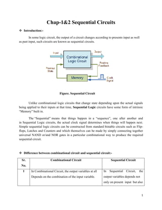
  • 1. 1 Chap-1&2 Sequential Circuits ❖ Introduction:- In some logic circuit, the output of a circuit changes according to presents input as well as past input, such circuits are known as sequential circuits. Figure. Sequential Circuit Unlike combinational logic circuits that change state depending upon the actual signals being applied to their inputs at that time, Sequential Logic circuits have some form of intrinsic “Memory” built in. The “Sequential” means that things happen in a “sequence”, one after another and in Sequential Logic circuits, the actual clock signal determines when things will happen next. Simple sequential logic circuits can be constructed from standard bistable circuits such as Flip- flops, Latches and Counters and which themselves can be made by simply connecting together universal NAND or/and NOR gates in a particular combinational way to produce the required sequential circuit. ❖ Difference between combinational circuit and sequential circuit:- Sr. No. Combinational Circuit Sequential Circuit 1 In Combinational Circuit, the output variables at all Depends on the combination of the input variable. In Sequential Circuit, the output variables depends not only on present input but also
  • 2. 2 depends upon the past input 2 Memory unit is not required in Combinational Circuit Memory unit is required to store the past input variable 3 The Combinational Circuits are faster Slower than Combinational Circuits 4 Combinational Circuits are easy to design Sequential Circuits are harder to design 5 Parallel adder is Combinational Circuit. Serial adder is a sequential circuit . ❖ Flip-Flops (F/F):- In a digital system, user requires the circuits whose output one’s set, should remain unchanged even if the input is changed. Such device can be used to store information in the form of binary number. The cross-coupled gates used to store binary data are known as flip-flops. In electronics, a flip-flop or latch is a circuit that has two stable states and can be used to store state information. A flip-flop is a bistable multivibrator. The circuit can be made to change state by signals applied to one or more control inputs and will have one or two outputs. It is the basic storage element in sequential logic. Flip-flops and latches are fundamental building blocks of digital electronics systems used in computers, communications, and many other types of systems. Flip-flops and latches are used as data storage elements. A flip-flop stores a single bit (binary digit) of data; one of its two states represents a "one" and the other represents a "zero". Such data storage can be used for storage of state, and such a circuit is described as sequential logic. There are different types of flip-flops are available such as: 1) RS flip-flop using NAND gate 2) RS flip-flop using NOR gate 3) Clocked RS flip-flop 4) JK flip-flop 5) Master – Slave JK flip-flop 6) D-type flip-flop 7) T-type Flip-flop.
  • 3. 3 I II 1) RS flip-flop using NAND gate:- Figure b) Truth Table S Q Q R Figure a) RS F/F using NAND gate The figure a) shows the logic diagram of RS F/F using NAND gates and figure b) shows the truth table of a RS F/F using NAND gate. When S=0, and R=0, both the gates output goes high (1). But these cannot be allowed because Q always has to be complemented of Q. When S=1, and R=0, now the output of gate-II is ‘1’. This is given as input to gate –I. So, gate-I receives both input as ‘1’, so output goes to ‘0’. Therefore, S=1, and R=0, the outputs are Q=0 and Q=1. When S=0, and R=1, the output of gate-I is ‘1’. This is given as input to gate-II. Thus, gate –II gets both inputs as ‘1’ so its output is ‘0’. Therefore, outputs are Q=1 and Q=0. When S=1, and R=1, we can’t decide the output unless we know the previous state, Suppose, the previous state is Q=1 and Q=0. So input to gate –I are (1,0) so output goes ‘1’. However, Q acts as a input to gate-II, so gate –II receives both inputs as (1,1), so it’s output goes to ‘0’. Therefore, S=1, and R=1, Q=1 and Q=0 which is nothing but previous state. 2) RS flip-flop using NOR gate:- S Q Q R Figure b) Truth Table R S Q 0 0 No Change 0 1 0 1 0 1 1 1 Invalid Figure a) RS F/F using NOR gate I II R S Q 0 0 Forbidden 0 1 0 1 0 1 1 1 No Change
  • 4. 4 The figure a) shows the logic diagram of RS F/F using NOR gates and figure b) shows the truth table of a RS F/F using NOR gate. When S=0, and R=0, we cannot go further unless we assume the previous state. Suppose, the previous state is Q=0 and Q=1. So input to gate –I are (0,1) so output goes ‘0’. However, Q acts as a input to gate-II, so gate –II receives both inputs as (0,0), so it’s output goes to ‘1’. Therefore, S=0, and R=0, Q=0 and Q=1 which is nothing but previous state (No change). When S=1, and R=0, now the output of gate-I is ‘0’. This is given as input to gate –II. So, gate-II receives both input as ‘0’, so output goes to ‘1’. Therefore, S=1, and R=0, the outputs are Q=0 and Q=1. When S=0, and R=1, the output of gate-II is ‘0’. This is given as input to gate-I. Thus, gate –I gets both inputs as ‘0’ so its output is ‘1’. Therefore, outputs are Q=1 and Q=0. When S=1, and R=1, the output of both NOR gates are becomes low (0), therefore, this is invalid output. 3) Clocked RS flip-flop:- Figure b) Truth Table Q Q Figure a) Clocked RS F/F using NAND gate The problem of an RS-F/F is that, there is no restriction on how fast the input can change, so it possible that input may vary faster than the propagation delay of F/F. Therefore, it is required to set or reset the F/Fs in synchronize with clock. This is achieved in clocked RS F/F’s. The above figure shows the clocked RS F/F. The inputs will be accepted when only when clock goes high. When Clock=1, S=0 and R=0, Here, outputs of gate A and B are high (1). So it can not workout further unless we know the previous state. Let us assume Q=0 and Q=1. Now, inputs to S A C Clock D R B R S Q 0 0 Qn 0 1 1 1 0 0 1 1 Qn
  • 5. 5 gate C are 1 and Q that is (1,1). Then output of gate C is ‘0’. This is given to input D gate. So inputs to D gate are (1,0) so output of D gate is ‘1’. Therefore, outputs are Q=0 and Q=1 , which is nothing but previous state or No Change(Qn). When Clock=1, S=1 and R=0, in this condition, output of gate A is ‘0’ and output of gate B is ‘1’. The gate C receives one of it input ‘0’, so its output becomes ‘1’. This output is given to input of D gate. So, the inputs to the D gate are (1,1). Thus, output of gate D goes ‘0’ . Therefore, output of the clocked RS f/F becomes Q=1 and Q=0. When Clock=1, S=0 and R=1, here output of gate A is ‘1’ and output of gate B is ‘0’. The gate D receives one of its input as ‘0’, So its output Q goes high(1). This is given to input of gate C . Now input to gate C are (1,1) so its output goes to zero. Therefore, output becomes Q=0 and Q=1. When Clock=1, S=1 and R=1, in this state we can’t decide the output unless we know the previous state. Suppose, the previous state is Q=1, Q=0. So the outputs of gate A and B are becomes ‘0’. Therefore, inputs to gate C are (0,0), so its output becomes ‘1’ , this is given to the gate D as an input. The inputs to gate D are (0,1), so its output becomes ‘1’. Therefore, output becomes Q=1 and Q=0 which is nothing but previous state. 4) JK flip-flop:- Figure. b) Truth Table Q Q Figure a) J K Flip-Flop The RS F/F has drawback that is when both inputs are high(1,1) the output is unpredictable. To eliminate this condition and to make the flip-flop to work even if the inputs are 1,1 the RS flip flop is modified and it becomes a JK flip flop. J A C Clock D K B Clock J K Q 1 0 0 Qn 1 0 1 0 1 1 0 1 1 1 1 Toggle
  • 6. 6 The above figure a) shows an JK flip flop using NAND gate and figure b) shows its truth table. In JK flip flop the output Q is fed as an additional input to gate A and Q is fed an additional input to gate B. To analyze the working one has to always know the previous state, consider the following cases:- Case-1: Clk=1, J=0, K=0, Assume Q=1 and Q = 0 The gate-A receives the inputs such as J, Clk and Q i.e 0,1,0 respectively , so the output of gate-A becomes ‘1’. The gate-B receives the inputs such as K, clk and Q i.e 0,1 and 1 respectively. The output of gate-B becomes ‘1’. The gate-C receives the input ‘1’ from gate –A and Q=0 , so output of gate-C becomes ‘1’ (Q). This ‘1’ is given as an input to gate D, therefore, gate D receives inputs ‘1’ from Q and ‘1’ from gate-B, so gate-D gives the output ‘0’. Hence at the output is Q=1 and Q=0 , which is nothing but assumed state or previous state. Case-2: Clk=1, J=0, K=1, last state Q=1 and Q = 0 The gate-A receives the inputs such as J, Clk and Q i.e 0,1,0 respectively , so the output of gate-A becomes ‘1’. The gate-B receives the inputs such as K, clk and Q i.e 1,1 and 1 respectively. The output of gate-B becomes ‘0’. The gate-D receives the one of its input ‘0’ from gate –B and Q=1 , so output of gate-D becomes ‘1’ (Q). This ‘1’ is given as an input to gate C, therefore, gate C receives inputs ‘1’ from Q and ‘1’ from gate-A, so gate-C gives the output ‘0’. Hence at the new output is Q=0 and Q=1. Case-3: Clk=1, J=1, K=0, last state Q=0 and Q = 1 The gate-A receives the inputs such as J, Clk and Q i.e 1,1,1 respectively , so the output of gate-A becomes ‘0’. The gate-B receives the inputs such as K, clk and Q i.e 0,1 and 0 respectively. The output of gate-B becomes ‘1’. The gate-C receives the one of its input ‘0’ from gate –A and Q=1 , so output of gate-C becomes ‘1’ (Q). This ‘1’ is given as an input to gate D, therefore, gate D receives inputs ‘1’ from Q and ‘1’ from gate-B, so gate-D gives the output ‘0’. Hence at the new output is Q=1 and Q=0. Case-4: Clk=1, J=1, K=1, last state Q=1 and Q = 0 The gate-A receives the inputs such as J, Clk and Q i.e 1,1,0 respectively , so the output of gate-A becomes ‘1’. The gate-B receives the inputs such as K, clk and Q i.e 1,1 and 1 respectively. The output of gate-B becomes ‘0’. The gate-D receives the one of its input ‘0’ from gate –B and Q=1 , so output of gate-D becomes ‘1’ (Q). This ‘1’ is given as an input to gate C, therefore, gate C receives inputs ‘1’ from Q and ‘1’ from gate-A, so gate-C gives the output ‘0’. Hence at the new output is Q=0 and Q=1. Therefore, in JK flip flop when both inputs are “1” it’s output toggle or complements to each other. Hence the drawback of an previous flip flops are removed.
  • 7. 7 ❖ Race Around Condition:- In JK flip flop, causes of an feedback connection at the input from output, one problem is occurs. For example:- J=1, K=1, Q=0, when the clock pulse is applied, the output becomes Q=1. This change take place after a time interval “ t” equal to the propagation delay. If the clock pulse is still there since, J=1, K=1 and Q=1 the output will become ‘0’ i.e Q=0. Thus for the duration of clock pulse, the output will oscillate in between 0 and 1 and at the end of cock pulse Q may be 0 or 1. This situation is known as Race Around condition t <tp< Tclock Tclock This race around condtion can be avoided by making the prorogation delay less than change in time it means that tp< t < Tclock 5) Master slave J K Flip Flop:- Q Q Figure Master Slave J K Flip-Flop The above figure shows the master slave J K flip flop. Here, J-K flip flop are cascaded, one works as master and another works as slave. The slave follows the master always. t tp J A C Qm E G Clock Master Clock Slave D K B Qm H F Clock
  • 8. 8 Dn Qn 1 1 0 0 Tn Qn 0 Qn 1 Qn D J Q D-Type F/F K Q Clock T J Q T-Type F/F K Q Clock While master accepting the new inputs, then at that time slave maintaining previous output as it is. When the master has completed the accepting the input, the slave will allow the changes cause by the master to reach the output. During this no new input are accepted by the master. So the output Q does not change during the propagation time of clock pulse and hence the race around difficulty is removed. When clock pulse is ‘0’ that is clock=0, so the master is disabled and clock=1 which causes slave is enable. The IC-7473 is dual JK flip flop is available in market. 6) D-Type Flip-Flop:- The JK flip flop is modified into D (Delay) flip flop by adding an inverter between J and K inputs, so that K is always complement of J. If the input is high (1), then J=1, k=0 and hence output Q=1, if D is 0 then J=0, K=1 and hence output becomes Q=0. The output Q after the clock pulse equals the input D. The D flip flop is used to provide a delay. 7)T-Type Flip-Flop: (Toggle):- The J K-flip flop is modified into T-type flip flop by connecting J and K together. This F/F changes the state with each clock pulse. It acts as a toggle switch and hence the name as T-type flips flop. When J=K=0 means T=0, then output is Qn and when
  • 9. 9 J=K=1 means T=1 then output is Qn. According to the truth table of J K flip flop the T-F/F is also known as complementing flip flop. ❖ IC – 7475(D-Flip Flop):- D1 D2 D3 D4 Clock1 Clock2 Q1 Q1 Q2 Q2 Q3 Q3 Q4 Q4 Vcc GND Figure . Pin diagram of IC-7475 It is a TTL IC working on +5V power supply. It is a quad bistable latch. It uses MSI technology (Medium Scale Integration Technology). It has four inputs (D-type), 8-outputs and two clock ‘s. One clock synchronizes two flip flops. In IC positive edge trigger is used. It is also called as transparent latch because as long s clock=1 all variations of D are passed on to the output. IC-7475 D-Type F/F CLK D Qn 0 x Last State 1 1 1 1 0 0
  • 10. 10 J QA J QB J QC J QD K K K K ❖ Counters:- One of the most famous sub systems in digital electronics is the Counter. The counter basically constructed using flip flops. The counters count the number of clock pulses arriving at its input. The output of the counter is binary or BCD equivalent of the number of clock pulses appeared at its input. The counter can be used as an instrument for measurement of time. ❖ Binary Counter / Ripple Counter / Asynchronous Counter(4-Bit): Vcc Clock QA QB QC QD Figure a) 4-bit binary counter 1 2 3 CLK 4 5 6 7 8 9 10 11 12 13 QA QB QC QD Figure b) Timing diagram of ripple counter F/F- D F/F- C F/F- B F/F- A
  • 11. 11 Figure.C) Truth Table Clock Pulses QD QC QB QA 0 0 0 0 0 1 0 0 0 1 2 0 0 1 0 3 0 0 1 1 4 0 1 0 0 5 0 1 0 1 6 0 1 1 0 7 0 1 1 1 8 1 0 0 0 9 1 0 0 1 10 1 0 1 0 11 1 0 1 1 12 1 1 0 0 13 1 1 0 1 14 1 1 1 0 15 1 1 1 1 The figure a) shows the binary counter or ripple counter in which flip-flop-A drives the flip- flop-B, flip-flop-B drives to flip-flop-C and flip-flop-C drives to flip-flop-D. The J and K inputs of all the flip-flop are connected to Vcc that is JK flip-flop is converted to T-type in which each flip-flop changes the step with a negative transmission of its clock input. When clock pulse is applied and when it goes negative, flip-flop-A changes the state. Flip- flop-A has to change the state to trigger flip-flop-B. Flip-flop-B has to change the state before it can trigger flip-flop-C, flip-flop-C has to change the state before it can trigger flip-flop-D. The trigger moves through the flip-flop’s like a ripple in water. The counters in which the output of one flip-flop drives another flip-flop are called Ripple counter or asynchronous counter. Initially all the flip-flop are reset, i.e QD QC QB QA = 0000. When the first clock pulse is applied flip-flop-A changes it state on the negative going part of the pulse. The flip-flop-A output goes from logic’0’ to logic ’1’, which is positive change and hence flip-flop-B does not respond to it. Since flip-flop-B has not change it’s state, flip-flop-C will not change it’s state, since flip-flop-C has not changed, flip-flop-D will not change. So at the end of first clock cycle the output condition is QD QC QB QA = 0001. When the 2nd clock pulse is applied flip-flop-A changes it state on the negative going part of the pulse. The flip-flop-A output goes from logic’1’ to logic ’0’, which is negative change. This negative change trigger flip-flop-B. Therefore, flip-flop-B goes from logic’0’ to logic ’1’ this is positive change in which has no effect on flip-flop-C, since flip-flop-C has not changed, so flip-
  • 12. 12 J QA J QB J QC K K K flop-D will not change. So at the end of second clock cycle the output condition is QD QC QB QA = 0010. When 3rd clock pulse is applied, flip-flop-A changes it’s state from ‘0’ to ‘1’ , this is positive going change and has no effect on the flip-flop-B. The flip-flop-B has not changed and hence flip-flop-C and flip-flop-D will not change. So at the end of third clock pulse the output condition is QD QC QB QA = 0011. So we can Say that, the output condition of 4th flip-flop is binary equivalent of number of clock pulses applied at it’s input. ❖ 3-Bit Asynchronous Binary Counter(UP-Counter):- (Ripple Counter) Vcc Clock QA QB QC Figure a) 3-bit asynchronous up counter 1 2 3 CLK 4 5 6 7 QA QB QC Figure b) Timing diagram of 3-Bit UP counter F/F- C F/F- B F/F- A
  • 13. 13 Clock Pulse QC QB QA 0 0 0 0 1 0 0 1 2 0 1 0 3 0 1 1 4 1 0 0 5 1 0 1 6 1 1 0 7 1 1 1 The figure a) shows the 3-bit binary counter in which flip-flop-A drives the flip-flop-B, flip- flop-B drives to flip-flop-C and flip-flop-C. The J and K inputs of all the flip-flop are connected to Vcc that is JK flip-flop is converted to T-type in which each flip-flop changes the step with a negative transmission of its clock input. When clock pulse is applied and when it goes negative, flip-flop-A changes the state. Flip- flop-A has to change the state to trigger flip-flop-B. Flip-flop-B has to change the state before it can trigger flip-flop-C. Initially all the flip-flop are reset, i.e QC QB QA = 000. When the first clock pulse is applied flip-flop-A changes it state on the negative going part of the pulse. The flip-flop-A output goes from logic’0’ to logic ’1’, which is positive change and hence flip-flop-B does not respond to it. Since flip-flop-B has not change it’s state, flip-flop-C will not change it’s state, since flip-flop-C has not changed. So at the end of first clock cycle the output condition is QC QB QA = 001. When the 2nd clock pulse is applied flip-flop-A changes it state on the negative going part of the pulse. The flip-flop-A output goes from logic’1’ to logic ’0’, which is negative change. This negative change trigger flip-flop-B. Therefore, flip-flop-B goes from logic’0’ to logic ’1’ this is positive change in which has no effect on flip-flop-C, since flip-flop-C has not changed, so at the end of second clock cycle the output condition is QC QB QA = 010. When 3rd clock pulse is applied, flip-flop-A changes it’s state from ‘0’ to ‘1’ , this is positive going change and has no effect on the flip-flop-B. The flip-flop-B has not changed and hence flip-flop-C will not change. So at the end of third clock pulse the output condition is QC QB QA = 011. So we can Say that, the output condition of 4th flip-flop is binary equivalent of number of clock pulses applied at it’s input.
  • 14. 14 ❖ 3-Bit Asynchronous down Counter:- Vcc Clock J QB F/F- B J QC F/F- C K QB K QC QA QB QC Figure a) 3-bit binary down counter 7 6 5 CLK 4 3 2 1 0 QA QB QC Figure b) Timing diagram of 3-Bit down counter Clock Pulse QC QB QA 0 0 0 0 1 0 0 1 2 0 1 0 3 0 1 1 4 1 0 0 5 1 0 1 6 1 1 0 7 1 1 1 QA K F/F- A QA J
  • 15. 15 The down counters are useful to count down sequences. The count sequences n, n-1, n- 2….1,0 etc upon receiving the next clock pulse, if the content of counter decreases then it is known as down counter. The above figure shows the 3-bit counter. The 3-bit down counter obtained using 3-flip-flops. The system clock is still applied at flip-flop-A. The QA, is used to drive flip-flop-B and QB is used to drive flip-flop. Initially, all the flip-flop are received 000, when the first clock pulse is applied, flip-flop-A toggles at negative edge of the pulse and QA becomes ‘1’. As QA goes from ‘0’ to ‘1’, QA goes from ‘1’ to ‘0’, which is negative change and it triggers flip-flop-B, causes of this QB goes from ‘0’ to ‘1’ and QB from ‘1’ to ‘0’ which is negative change and it further triggers flip flop-C. The end of the clock pulse, the output condition is QC QB QA = 111. When second clock pulse is applied at the negative edge, flip flop-A toggles, so QA output goes from ‘1’ to ‘0’, QA goes from ‘0’ to ‘1’ which is positive changes and it does not affect flip- flop-B. Since flip flop-B has not change, flip flop-C will not change, so at the end of second clock pulse output is QC QB QA = 110 and so on. ❖ 3-Bit UP / Down Counter:-
  • 16. 16 As we know, the separate circuit of up counter and down counter, by using some gating circuit it is possible to connect either Q or Q at the clock input of next flip-flop and hence single circuit can be used as either up counter and down counter. Such a circuit which can be used as up counter and down counter. When the count of line is high(1) and countdown line is low(0), Q output of previous flip flop gates connected to the clock input of next flip flop. Then the circuit behaves as the up counter. Where, as when count line is low and countdown is high, then Q output of previous flip flop gates connected to clock input of next flip-flop and circuit behave as the down counter.
  • 17. 17 ❖ Modulus Counter:- The modulus counter tells us the number of states the counter can count, for example, MOD- 10 counter means it can count 10 states; similarly, MOD-8 counter can count 8 states. If ‘m’ is the number of states to be counted and ‘n’ be the number of flip-flops, then the relation is m<=2n . Thus, 4-flip-flops are required for MOD-9 to MOD-16 counters. Similarlly, 3-f/F are required for MOD-5 to MOD-8 counter. Synchronous Counters: ❖ MOD-8 Synchronous Counter :- 3 Bit Synchronous Up Counter
  • 18. 18 Clock Pulse QC QB QA 0 0 0 0 1 0 0 1 2 0 1 0 3 0 1 1 4 1 0 0 5 1 0 1 6 1 1 0 7 1 1 1 The above figure a) shows the 3-bit synchronous counter. The speed of operation improves significantly if all the flip-flops are clocked simultaneously. The resulting circuit is known as synchronous counter. The output of flip-flop-A changes for every clock pulse. This can be achieved by using a T-type flip-flop with T0=1(Vcc). The output of QB changes whenever, QA changes from 1 to 0 (at negative change). According to the truth table of T-type flip-flop, T is ‘0’ then output will not change and when T=1 and clock pulse is applied then output is complemented. Synchronous Binary Down Counter An ‘N’ bit Synchronous binary down counter consists of ‘N’ T flip-flops. It counts from 2𝑁 − 1 to 0. The block diagram of 3-bit Synchronous binary down counter is shown in the following figure. The 3-bit Synchronous binary down counter contains three T flip-flops & one 2-input AND gate. All these flip- flops are negative edge triggered and the outputs of flip-flops change affectaffect synchronously. The T inputs of first, second and third flip-flops are 1, Q0′Q0′ &' Q1′Q1′Q0′Q0′ respectively. The output of first T flip-flop toggles for every negative edge of clock signal. The output of second T flip-flop toggles for every negative edge of clock signal if Q0′Q0′ is 1. The output of third T flip-flop toggles for every negative edge of clock signal if both Q1′Q1′ & Q0′Q0′ are 1.
  • 19. 19 ❖ Comparison between synchronous counter and asynchronous counter :- Sr. No. Synchronous counter Asynchronous counter 1 Every F/F triggers by the clock. Therefore, they make their transition simultaneously The clock pulse is applied to clock input of first F/F only. 2 Delay time is less at is equal to single F/F only Delay time is more at is equal to the sum of total number of F/F. 3 Speed of operation is more and can be operated with high frequency. Speed of operation is limited. The highest clock frequency depends on overall system. 4 Circuit is complex, more hardware is required and hence cost is more. Simple circuit, easy to design, less hardware is required and hence cost is less.
  • 20. 1 Electronic Science Digital Electronics 20. Shift Register Module-20 Shift Registers 1. Introduction 2. Types of shift registers 2.1 Serial In Serial Out (SISO) register 2.2 Serial In Parallel Out (SIPO) register 2.3 Parallel In Parallel Out (PIPO) register 2.4 Parallel In Serial Out (PISO) register 3. Bidirectional shift register 4. Universal shift register 5. Ring counter 6. Johnson counter 7. Shift register ICs 8. Applications of shift registers 9. Summary Learning Objectives: 1. To study the data shift/transfer in different registers 2. To understand the construction and working of different shift registers. 3. To learn the sequence of operation of Ring and Johnson counter 4. To know the applications of shift registers.
  • 21. 2 Electronic Science Digital Electronics 20. Shift Register 1. Introduction In almost all cities, we see various big rolling displays advertising different products or sales. This is one of the most popular applications of shift register. Text/image can enter from left or right and moves out sequentially. Similarly, data can be loaded inparallel from top and leaves towards bottom. For long distance data communication, shift register can convert slow parallel data into high speed serial over single wire and serial to parallel at a receiver end. This helps in reducing the cost of data transmission. Shift registers like counters are basically some form of sequential circuit. Unlike combinational circuit, sequential circuit outputs are not only dependent of present inputs but also on the past inputs as well. Flip flops are used for storing binary information. Single flip flop can store 1-bit binary data either 0 or 1. To increase the storage capacity, we need to use group of flip flops. Register is a group of flip flops connected together to store multiple bits. The n-bit register consist of n number of flip flops and is capable of storing n-bit information. For example 8-bit register can store 8-bit data for a computer and requires 8 flip flops. Binary data can be entered serially or parallel into the register. Similarly, the data can be shifted out in serial or parallel out on every clock pulse. Shift registers are classified into 4 types depending upon how the data is shifted in and shifted out either serially or parallel. In addition, there are bidirectional shift registers, ring and Johnson counter. There are MSI shift registers available commercially in TTL as well as in CMOS families. Let us now study the shift registers in this module. 2. Types of shift registers Shift registers are a type of sequential logic circuit. Shift register has two important keywords. The first one is shift and the second is register. Register is basically a group of flip flops connected in such a way that binary number can be entered into the register. Single flip flop can store only ‘1’bit data. For storing ‘n’-bits, n flip flops are required for storage. Shift register is capable of storage as well as shift or data transfer. For handling the binary data, there are two main operations Shift-In for data entry and Shift- Out for data transfer or exit. Both the operations can be implemented either bit by bit i.e. serially or all-bits-simultaneously i.e. in parallel.
  • 22. 3 Electronic Science Digital Electronics 20. Shift Register Figure 1: Types of shift registers Shift registers can have serial or parallel inputs and outputs. There are some shift registers that have both serial and parallel inputs and outputs as shown in figure 1. Classification of shift register depends on how the data is shifted IN and shifted-OUT i.e. whether the data input and output are serial or parallel. There are four basic types of shift registers: 1. Serial In Serial Out (SISO) shift register 2. Serial In Parallel Out (SIPO) shift register 3. Parallel In Serial Out (PISO) shift register 4. Parallel In Parallel Out (PIPO) shift register When the data is to be moved serially both at the input or output, the type of shift register used is serial in serial out (SISO). If the data is fed serially at the input and is retrieved in parallel manner at the output, the shift register is known as serial in parallel out (PISO). This action results in serial to parallel conversion. When data is entered in parallel and taken out in a serial fashion, the shift register is called parallel in serial out (PISO) register. This shift register is also called parallel to serial converter. Finally, if both the input and output are in parallel manner, the shift register is termed as parallel in parallel out(PIPO) register. In all four types, the storage as well as transfer of data takes place only upon the applications of clock pulses. When the clock is absent, the original data is retained till power is on and shift register acts like a temporary memory.
  • 23. 4 Electronic Science Digital Electronics 20. Shift Register Figure 2: Different ways to transfer/move data The possible ways of data movements in a shift register are shown in figure 2. Registers are implemented using flip flops that provide storage capacity. In this case, a 4-bit shift register is used for shift and storage. The arrow indicates the direction and type of data transfer. Data is entered serially and shifted right or left. It is also possible to introduce rotate right or left operation using closed loop path. Serial operation requires at least four clock pulses for 4-bit register to shift the data to left or right. For faster operation, data can be entered in using parallel shift in operation or parallel shift out in single clock cycle. Basic elements of shift register Figure 3: SR, D and JK flip flops as basic elements of shift register Shift registers can be constructed using simple SR, D or JK flip flops. Figure 3 indicates the FFs as the basic elements of shift register. Flip flops can be either positive or negative edge triggered flip flop. In case of counter, JK flip flops are usually used in toggle mode of operation. Whereas in a shift register, it is possible to use SR, JK or D flip flop in set, reset or hold mode. Single flip flop acts as a 1-bit storage register. With the proper interconnections of the flip flops it is possible to decide the type and storage capacity of the shift register. In the next section, let us discuss the construction and working of different types of shift registers.
  • 24. 5 Electronic Science Digital Electronics 20. Shift Register 2.1 Serial In Serial Out (SISO) shift register The serial in serial out (SISO) shift register is a simply collection of clocked flip flops linearly connected. This register accepts data serially (one bit at a time) and shifts or moves the data serially through various stages of the registers and exits form last flip flop serially. Figure 4: Serial In Serial Out shift register Let us consider a 4 bit shift register constructed using four D-flip flop in cascade as shown in figure 4. External serial data is fed to the first D flip flop and data exits serially from the fourth i.e. last flip flop. Each flip flop has its outputs connected to the inputs of the next in line. The same clock input goes to all flip –flops and they are all negative edge triggered. Let us study the operation of SISO register. The shift register is initially in clear state i.e.(Q0 Q1 Q2 Q3= 0000). Consider data to be entered as 0101. Data must be entered beginning with right most bit first (LSB). The serial data input ‘1’ is applied to the first FF. When the first clock pulse is applied, the first FF output becomes Q0=1. The register contains now 1000. Now the second bit is applied to the data input. D=0 for first flip flop and D=1 for the second flip flop. When second clock pulse is applied, at negative transition, The second FF output Q1 changes to 1 and Q0 becomes 0. The register contains now 0100. The third bit 1 at serial input is allowed to store in the first FF with the third clock pulse. The 0 stored in first FF is shifted to second flip flop and 1 stored in second flip flop is shifted to third flip flop. The register output is 1010. With the fourth clock pulse, the last bit 0 is present at serial input and is shifted into first flip flop and Q0 becomes 0. Bit stored in first FF is shifted to second FF i.e. 1. The 0 stored in second FF is shifted to third FF. The LSB =1 stored in third FF is shifted to last FF. The register now contains 0101. After shift in operation, first (right most) bit of serial data is available at the serial data output. The second data bit is shifted out at the next clock transition. Similarly third bit is also shifted out and last bit is available with next clock transition The register is of right shift type and the stored data is shifted out of the right and lost after eight clock cycles. Let us summarize the operation. In SISO register, first bit is entered into the register on the first clock pulse and then shifted from left to right as remaining bits are entered and shifted. In such register, for serial data one bit at a time is transferred into or out of the register. Therefore, 4 clock pulses are required to transfer the data into the register and additional 3 clock pulses are required to shift data out of the register serially.
  • 25. 6 Electronic Science Digital Electronics 20. Shift Register 2.2 Serial In Parallel Out (SIPO) shift register Figure 5: Serial In Parallel Out shift register For a 4-bit SIPO shift register, there is one data input, 4-outputs and one clock input as shown in figure 5. In such register the data is enter serially just similar to SISO shift register. First bit is entered into the register on the first clock pulse and then shifted from left to right as remaining bits are entered and shifted. In such register, for serial data one bit at a time is transferred into the register. Therefore, 4 clock pulses are required to transfer the data into the register. There is difference in a way the data bits are shifted out of the register. Once the data are stored in the register, each bit appears on respective output lines of flip flops. As all bits are available simultaneously, the shift register provides parallel out lines. 2.2 Parallel In Serial Out (PISO) shift register This type of shift register accepts data in parallel form and outputs it in serial form. With a single clock pulse, data bits are entered simultaneously into the respective flip flop stages of the shift register and output is available bit by bit from last storage. For PISO register, it is necessary to shift the data after loading it in parallel. But unfortunately, the two acts - parallel loading and shifting serially cannot occur simultaneously. This is achieved using AND-OR logic as shown in figure 6. Figure 6: Combinational block for PISO shift register
  • 26. 7 Electronic Science Digital Electronics 20. Shift Register There are two AND gates. One of them receives parallel data bit and the other receives output of previous FF for shifting. The other input controls whether data should be loaded in parallel or to be shifted. The output of OR gate is connected to input of next FF. This OR gate allows either Parallel load or shift data. Figure 7: Parallel In Serial Out Shift register This register consists of 4 D flip flops. All flip flops are triggered simultaneously by a common clock. There are four parallel data inputs ABCD applied to the register. Parallel data bits and outputs of previous stage are given as inputs to two AND gates. Other input comes from direct control and inverted control as shown here. Outputs of the two AND gates act as inputs for the OR gate whose output is fed as input to the next stage of shift register as shown in figure 7. Let us consider parallel data ABCD=0101. When the control line LOW, second AND gate is enabled and first AND is disabled. So parallel data bit appears as data input. Application of one clock pulse now allows this parallel data to be stored into the 4-bit register. Advantage of this configuration is that any number of bits are transferred into the register in a single clock pulse. With one clock pulse the parallel data available at D input appears at the output of register. On the other hand, when control line is HIGH, first AND gate is enabled i.e. the Q output of previous FF appears as data input to the next stage. Here, four clock pulses are required to shift the data out of the register serially. The output of last FF Q3 acts as a serial data output of the shift register. 2.4 Parallel In Parallel Out (PIPO) shift register In the 4 bit parallel in parallel out shift register, four independent D flip are used as shown in figure 8. The D inputs are acting as the parallel inputs and Q outputs of the FFs act as the parallel outputs of the shift register. Let us consider the parallel data ABCD = 0101.
  • 27. 8 Electronic Science Digital Electronics 20. Shift Register Figure 8: Parallel In Parallel Out Shift Register The clock inputs of all FFs are triggered by a single clock signal. Once the register is clocked, all the data at the D inputs appear at corresponding Q outputs of the FFs simultaneously. This shift register requires only one clock pulse for operation; hence it is the fastest shift register. 3. Bidirectional shift register It is the shift register in which the data can be shifted either left or right. The four bit bidirectional shift register using D flip flops is shown in figure 9. There are two AND gates and a OR gate used at the input of each D flip flop. This combinational circuit allows the serial data to be shifted left or right based on the Left/Right shift control pin. Figure 9: Bidirectional shift register Let us consider a binary data 1101 applied to the serial data in for left shift. The left’/Right input is set to 0. With this control input, the inverter produces 1 at the output which enables the second AND gates of the combinational circuit. This allows data present at second AND gate to pass through OR gate to D inputs of the FFs. The D input of FF4 receives the serial data; D input of FF3 receives Q3 output; D input of FF2 receives Q2 output and D input of FF1 receives Q1 output.
  • 28. 9 Electronic Science Digital Electronics 20. Shift Register Application of a clock pulse shifts the data to the left by 1 bit position. After four clock pulses, the output of left shift register contains the data 1101. It further requires 3 clock pulses to shift the data out serially from Q0 of the left shift register. Let us consider a binary data 0101 applied to the serial data in for right shift. The left’/Right input is set to 1. With this control input, the first AND gates of the combinational circuit is enabled. This allows data present at first AND gate to pass through OR gate to D inputs of the FFs. The D input of FF1 receives the serial data input; D input of FF2 receives Q0 output; D input of FF3 receives Q1 output and D input of FF4 receives Q2 output. Application of a clock pulse shifts the data to the right by 1 bit position. After four clock pulses, the output of right shift register contains the data 0101. It further requires 3 clock pulses to shift the data out serially from Q3 of the right shift register. 4. Universal shift register A universal shift register can transfer data in three different modes. It can load and transmit data in parallel. It can load and transmit data in serial fashion, through left shifts or right shift. This allows user to activate either SISO, SIPO, PISO and PIPO shift register. 4bit Universal shift register consist of 4 positive or negative edge triggered D flip flops. To load and transmit the data in parallel or serial fashion, there is a AND-OR combinational circuit at D input of every flip flop as shown in figure 10. Figure 10: Universal shift register Serial in or serial out can be implemented by shifting the data in any one of the two directions. Left shift requires Q0Q1Q2Q3serial Data in whereas the right shift requires Serial data in Q0 Q1Q2Q3. For SISO, the shift in operation needs shift/load input connected to HIGH state and will take 4 clock pulses to shift the data serially in. The shift out operation also need shift/load input kept connected to HIGH state and will require 3 clock pulses shift data serially out. This is because the output already has LSB before shift out operation begins. For SIPO, the Shift/load operation is connected at HIGH state and will require no clock pulse to take the data is already available at the outputs.
  • 29. 10 Electronic Science Digital Electronics 20. Shift Register Type Shift In Shift Out Shift/Load Number Of Clock Pulses Shift/Load Number Of Clock Pulses Right shift SISO 1 4 1 3 SIPO 1 4 1 0 PISO 0 1 1 3 PIPO 0 1 0 0 Left shift SISO 0 4 0 3 Figure 11: Functional table for universal shift register For PISO operation, shift/load input be connected to LOW state to enable parallel load operation. For shift out operation, the shift/load input must be connected to HIGH state for shift serial OUT and will require 3 pulses again. For PIPO operation, shift/load input be connected to LOW state to enable parallel load operation and requires only 1 clock pulse to load the data in parallel and no clock pulse to take the data at output since it is always available at the output. For shift left operation, parallel data input (Dn) receives Qn+1 output, hence shift/load be connected to low state for both modes. 5. Ring counter Ring counter is a type of shift register with the output of the last flip flop is fed back to the input of the first flip flop. The data stored within the shift register will circulate as long as clock pulses are applied. The 4-bit ring counter consists of four D flip flops with clock input connected to the common clock. External RESET input is connected to Preset input of the first FF and Clear input of all remaining flip flops as shown in figure 12. Figure 12: Ring counter Let us understand the working of ring counter with the help of function table. Initially, an active LOW level is applied to Reset input, which sets Q0 as 1 and other flip flop outputs will be 0. The contents of the register are Q0Q1Q2Q3 =1000 as shown in figure 13.
  • 30. 11 Electronic Science Digital Electronics 20. Shift Register Clock pulse Q0 Q1 Q2 Q3 0 (Reset) 1 0 0 0 1 0 1 0 0 2 0 0 1 0 3 0 0 0 1 4 1 0 0 0 Figure 13: Operation of Ring counter Application of first clock pulse shifts the logic 1 to Q1 as D input of second FF is connected to Q0. The register now contains 0100. Application of second clock pulse shifts the logic 1 to Q2 as D input of third FF is connected to Q1. The register now contains 0010. Further application of third clock pulse shifts the logic 1 to Q3 as D input of fourth FF connected to Q2. The register now contains 0001. Forth clock pulse shifts the logic 1 to Q0 as D input of fourth FF connected to Q3. The register now contains 1000 again and ring counter operation continues further. 6. Johnson counter A Johnson counter is a modified ring counter in which the complemented output of the last flip flop is connected to the input of the first flip flop. Johnson counter is also called as twisted ring counter. Let us consider a 4-bit Johnson counter constructed using 4-D flip flops as shown in figure 14. The circular connection is made from complement output of the rightmost flip flop to the input of the leftmost D flip flop. The register shifts its contents one bit position to the right with every clock pulse and the complement value of last flip flop is transferred to the first flip flop at the same time. Figure 14 Johnson Counter Let us understand the working of Johnson counter. Initially, an active LOW level is applied to the clear input, which resets all the flip flops. Thus the register contains Q0Q1Q2Q3 =0000. With the first clock pulse, the first flip flop inserts 1 into the register as Q3’=1. The content of
  • 31. 12 Electronic Science Digital Electronics 20. Shift Register the counter are 1000. With the second clock pulse, new ‘1’ is added into the register as Q3’=1. The content of the counter is now 1100. Next clock pulse generates the counter contents as 1110. Fourth clock pulse shifts the whole contents to right and adds 1 to the left position. Thus we get 1111 as shown in figure 15. Clock pulse Q0 Q1 Q2 Q3 0 0 0 0 0 1 1 0 0 0 2 1 1 0 0 3 1 1 1 0 4 1 1 1 1 5 0 1 1 1 6 0 0 1 1 7 0 0 0 1 8 0 0 0 0 Figure 15: Operation of Johnson counter As Q3=1, the complement of Q3 is 0. Now the value ‘0’ is inserted into the register. Thus, with the next clock pulse, the counter contains 0111. Next counter becomes 0011 with next clock pulse. Further it becomes 0001 with the clock pulse. Finally the counter becomes 0000 with the clock pulse. Starting from the clear state, the Johnson counter goes through a sequence of 8 states. In general, a n-bit twisted ring Johnson counter will go through a sequence of 2xn states. The disadvantage of Johnson counter is that it does not count in binary sequence. 7. Shift register ICs There are several commercially available shift register ICs. These include right from simple serial in serial out shift register to universal shift register IC under TTL logic family as shown in figure 16. 7491 8 bit serial in / serial out shift register 7495 4-bit serial/parallel access shift register (Universal) 74164 8 bit serial in / parallel out shift register 74165 8 bit parallel load shift register 74166 8 bit parallel in serial out shift register 74174 6-bit parallel in parallel out shift register 74194 4 bit bidirectional universal shift register 74198 8 bit bidirectional universal shift register Figure 16: Table showing commercially available shift register ICs.
  • 32. 13 Electronic Science Digital Electronics 20. Shift Register 8. Applications of shift registers Shift register are used in variety of applications as listed below. 1. Delay line- The SISO register can be used to introduce time delay. The delay is proportional to number of flip flops. 2. Serial to parallel converter- Serial in parallel out (SIPO) shift register can be used to convert data in serial form to parallel form e.g. keyboard interfacing. 3. Parallel to serial converter- A parallel in serial out ( PISO ) shift register can be used to convert data in parallel form to serial form. This is required in a situation where parallel data transmission is not feasible at long distance e.g. modem/router interfacing. 4. Sequence generator- sequence to operate various electronic gadgets can be obtained using shift register 5. Ring counter - a particular set of control signals can be generated using ring counter. Shift register is also used in 6. Pulse train generator 7. Registers in processors 8. Keyboard encoding 9. Rolling display 10. Universal asynchronous receiver transmitter (UART) Let us now conclude this module by summarizing the important points in shift register. 9. Summary Shift registers are basically a sequential logic circuit capable of storing binary data. The data can be accepted either in serial or parallel fashion and similarly transfer the data either in serial or parallel format. There are four basic types of shift registers: SISO, SIPO, PISO, PIPO. Shift register are mainly constructed using either SR, JK or D flip flop. Bidirectional shift register can move the data either to left or right direction serially. Universal shift register is capable of performing all these data transfer capabilities. The Ring and Johnson counter are special shift registers. The ring counter has n states in sequence whereas Johnson counter has 2n states in the sequence.