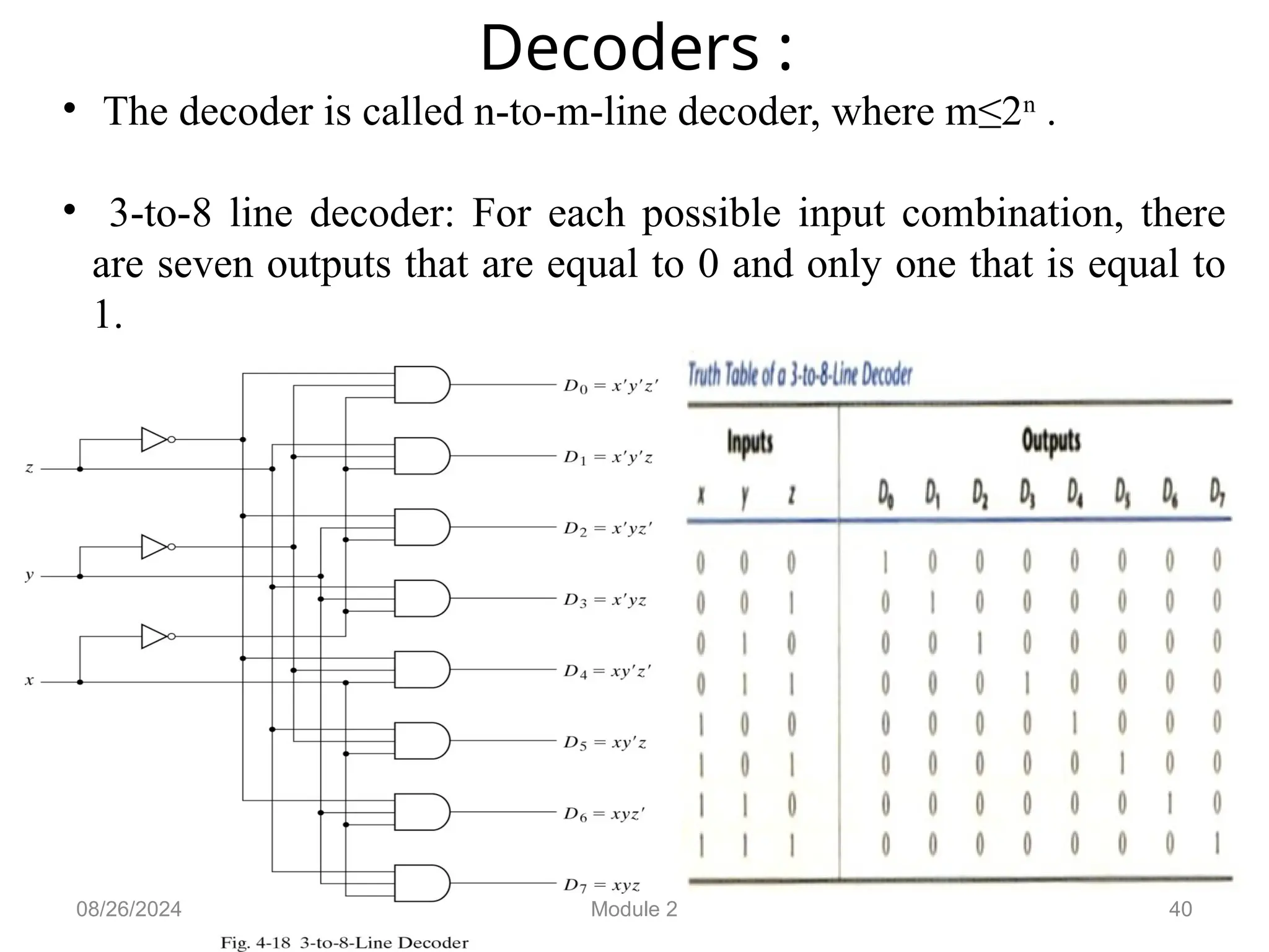
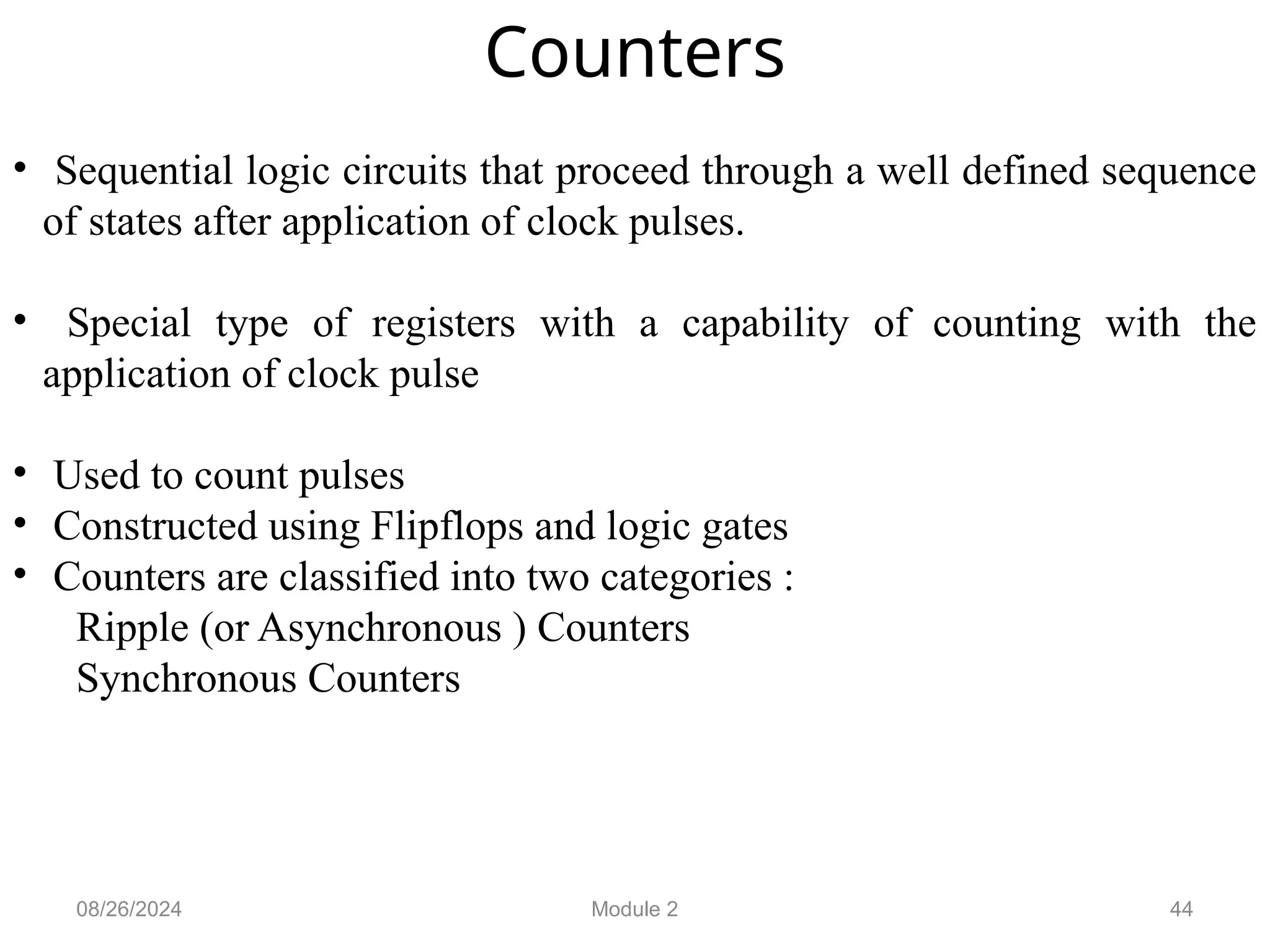
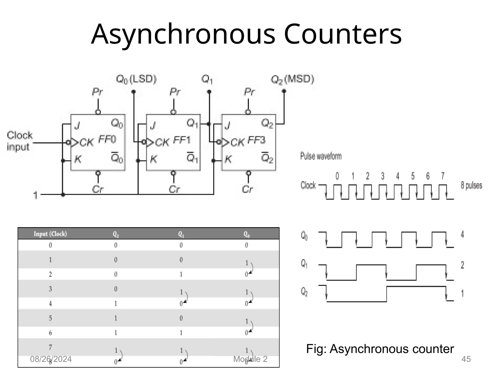
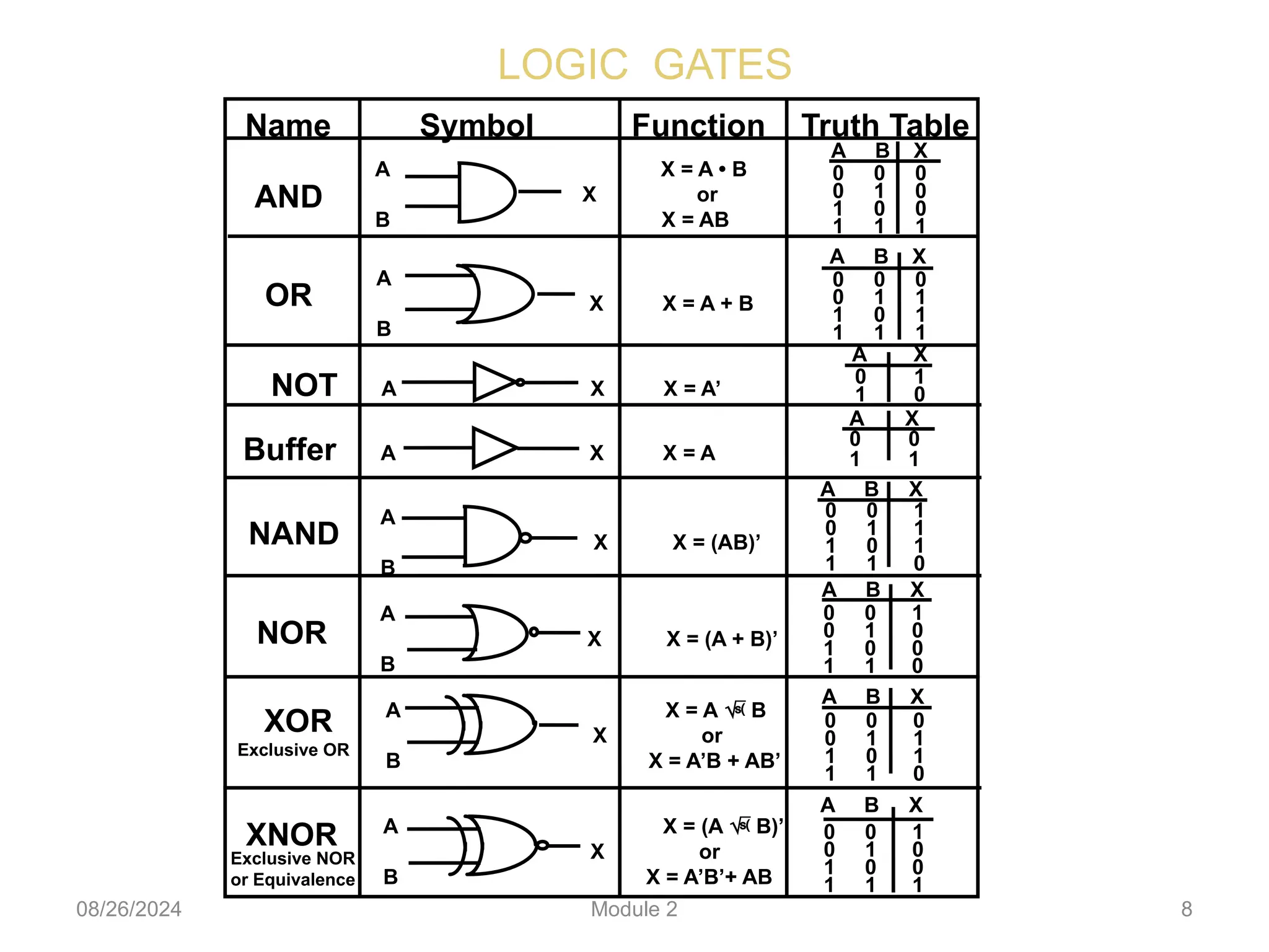
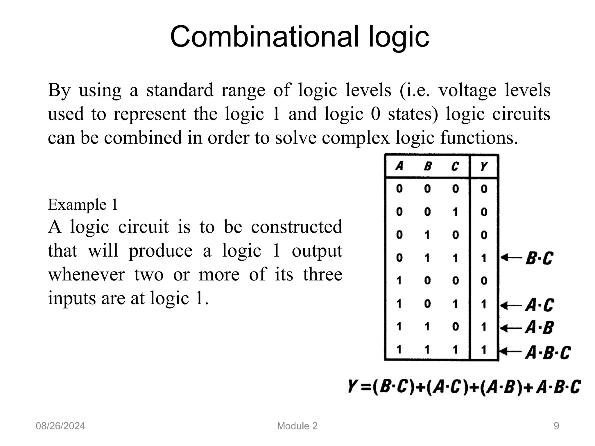
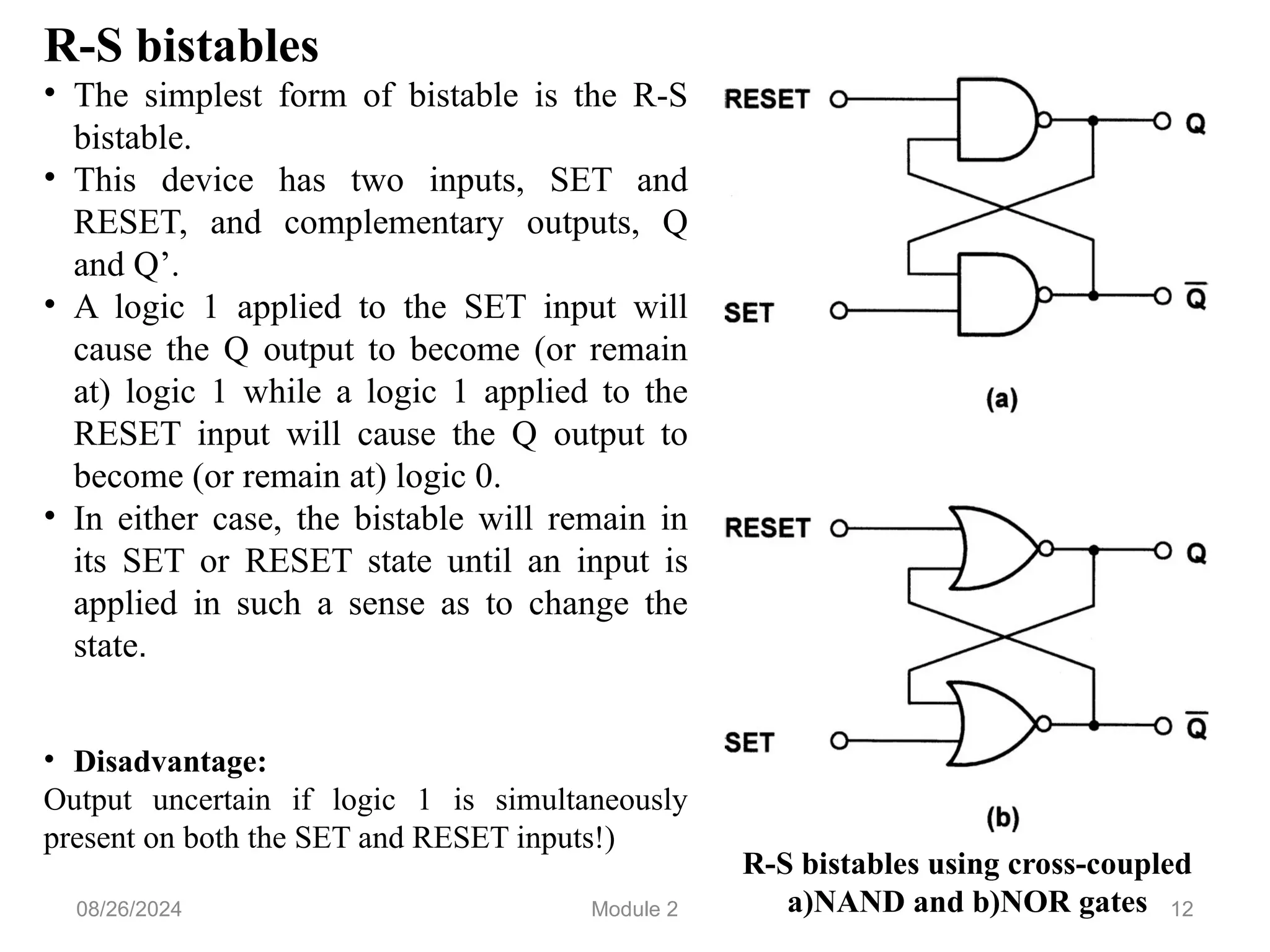
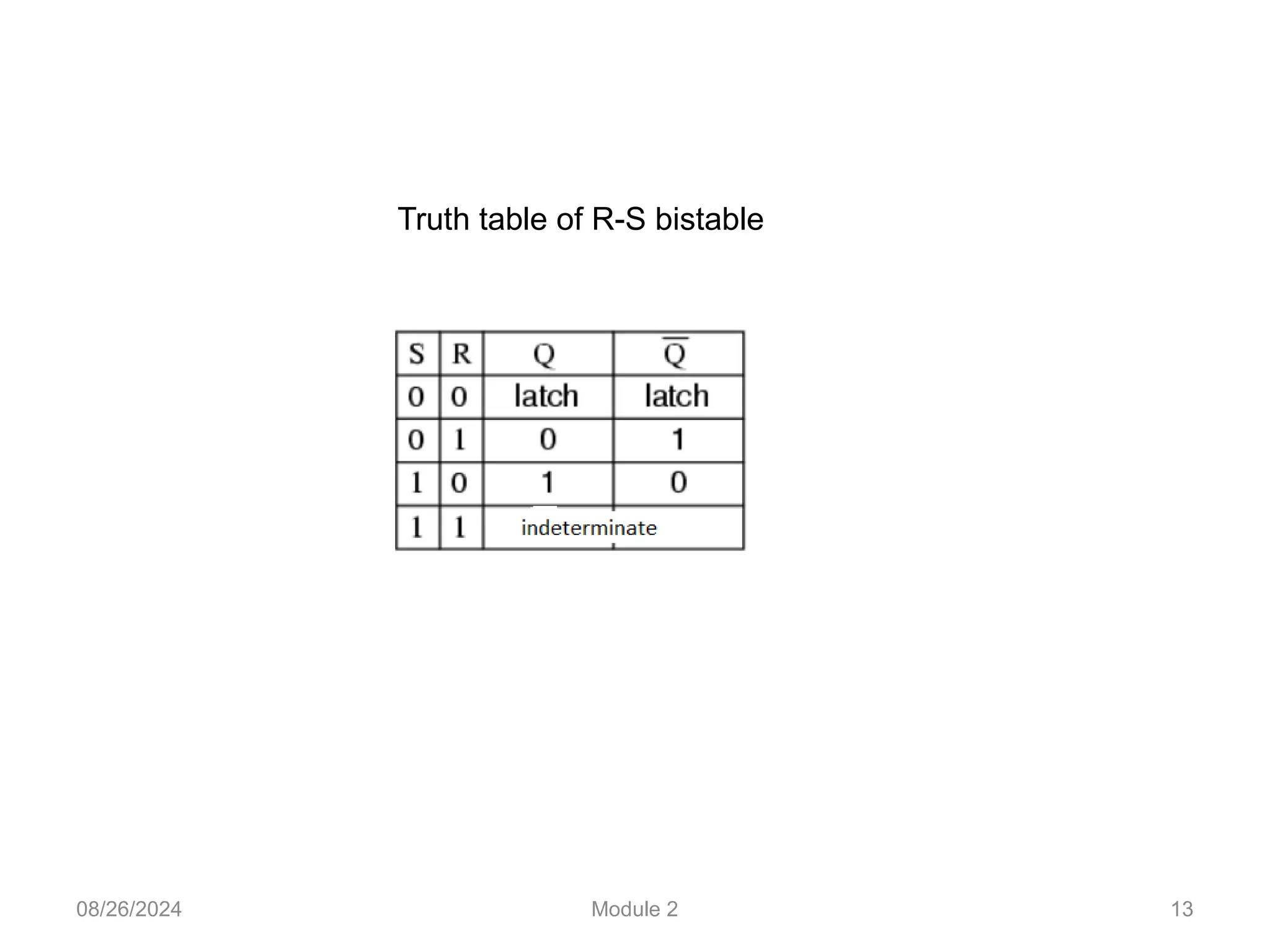
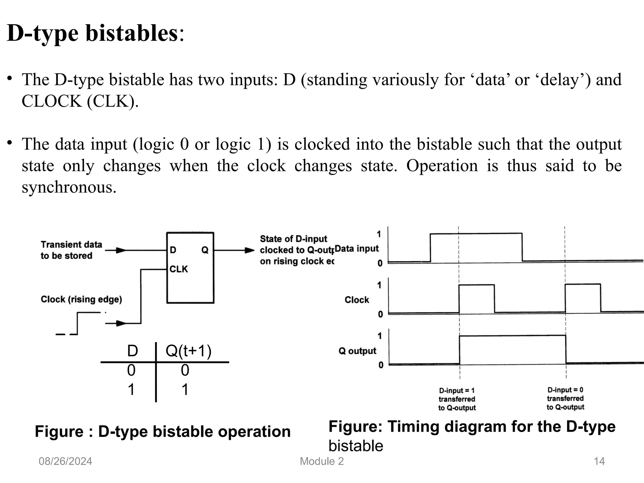
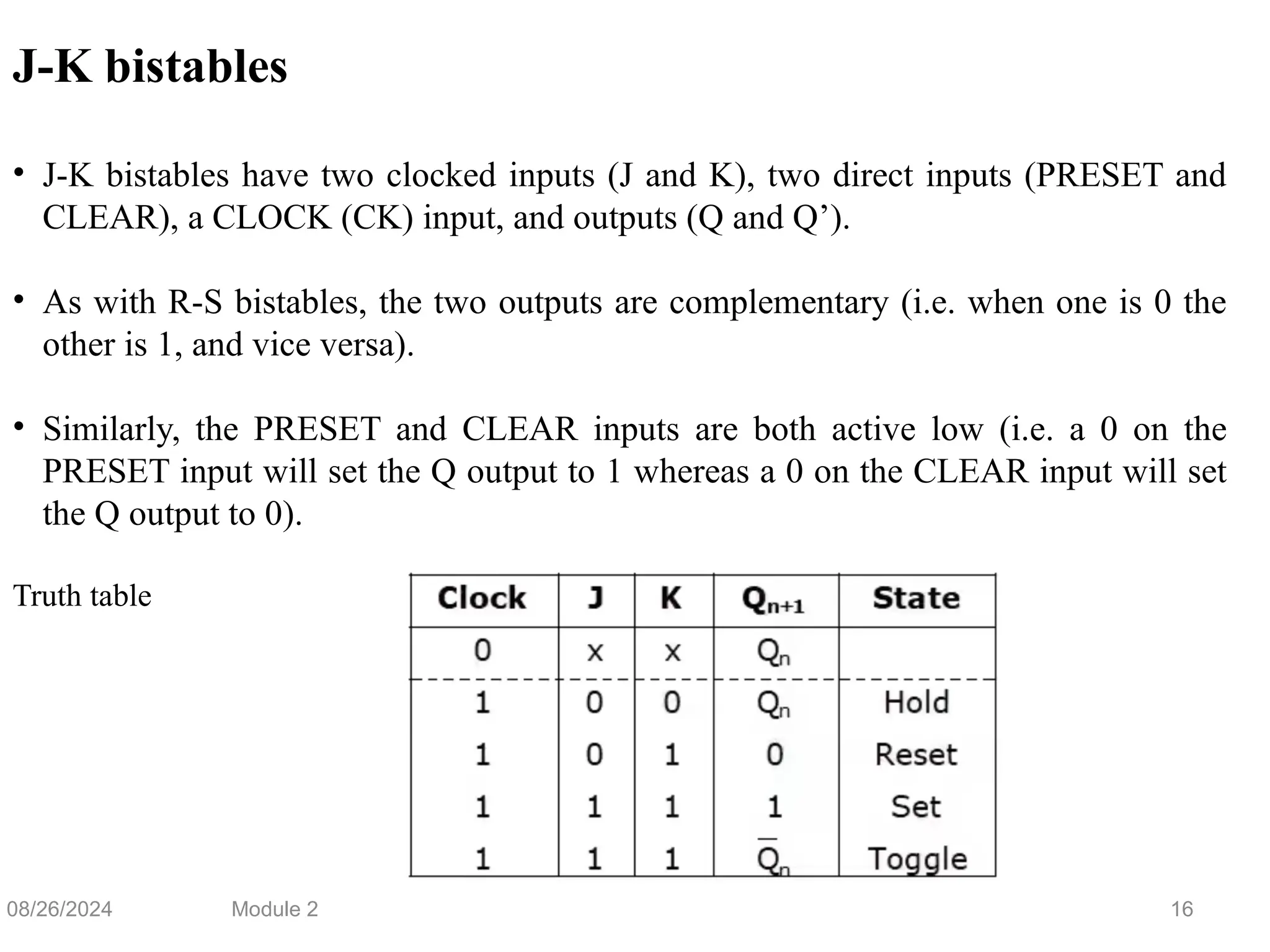
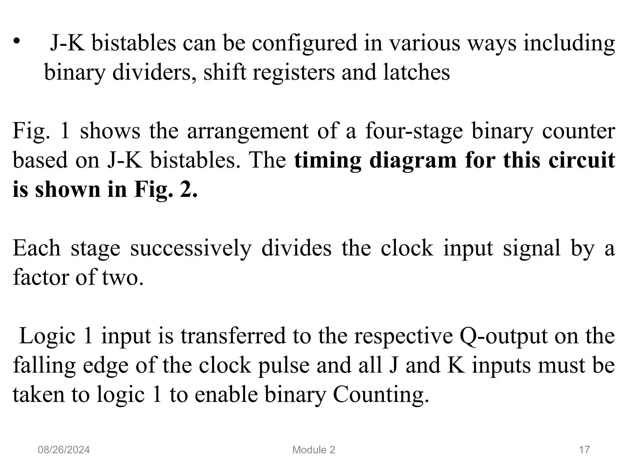
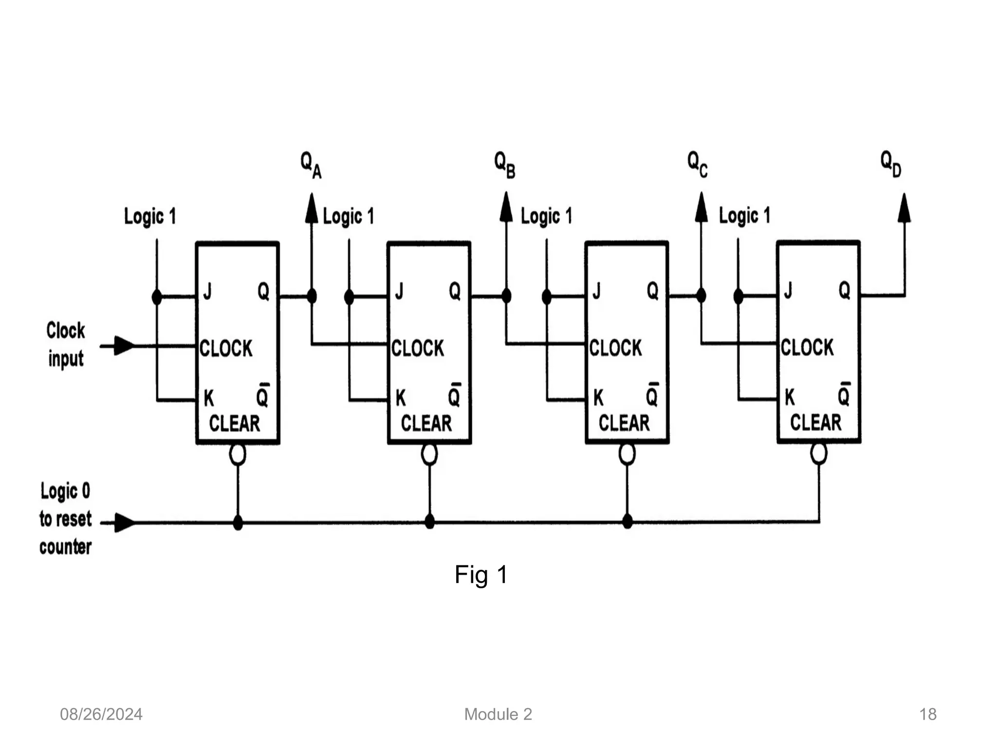
The document outlines the syllabus for a basic electronics course covering modules on electronic circuits, logic circuits, and embedded systems. It details fundamental concepts such as logic gates, bistables, and microcontroller operations, as well as design examples for various logic circuits and their applications. Additionally, it provides information on data representation, input/output devices, and components like multiplexers and decoders.
![08/26/2024 Module 2 31
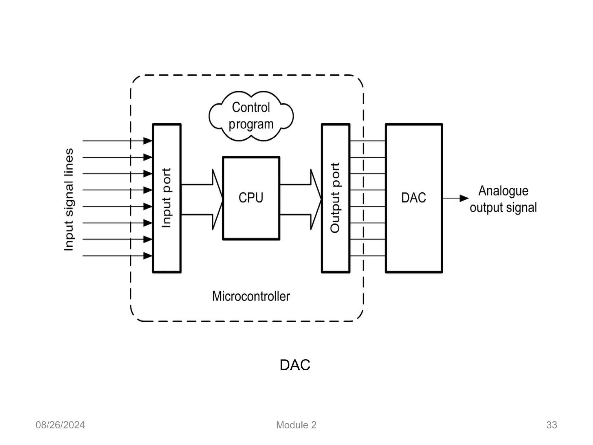
ADC [1]](https://image.slidesharecdn.com/bec-module2-digitalelectronics-240826104326-1cdc9faa/75/Digital-electronics-as-an-emerging-field-pptx-31-2048.jpg)
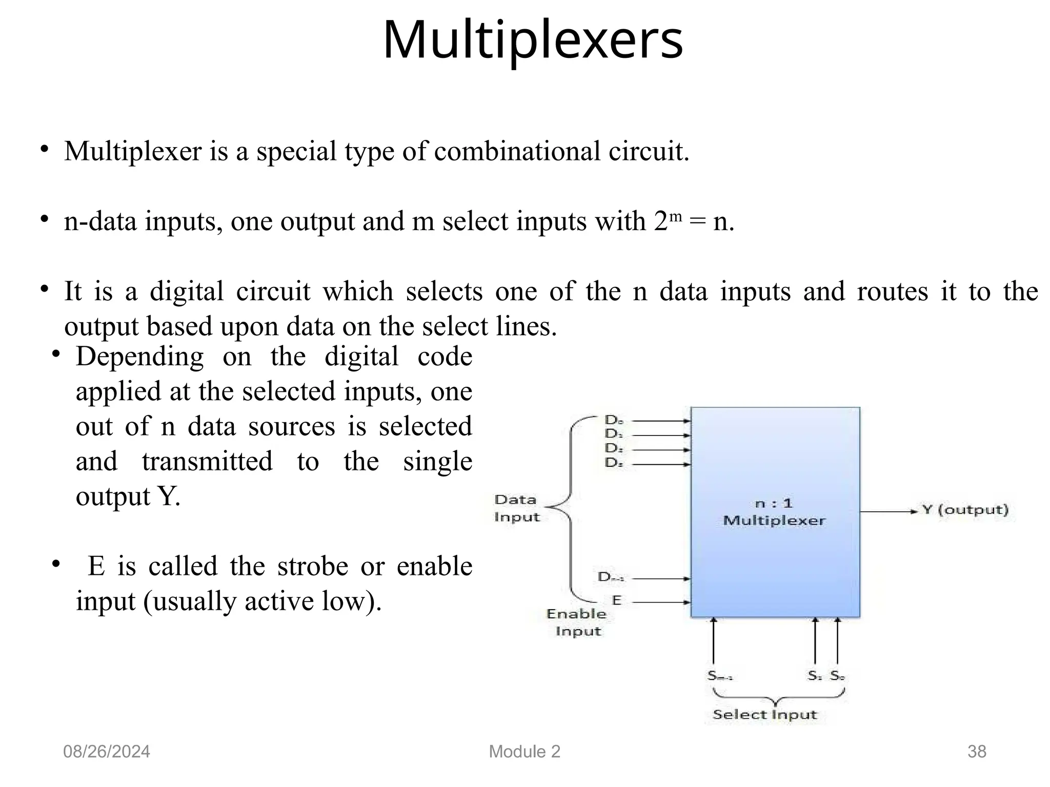
![39
8:1 Multiplexer
Fig reference: [2]
08/26/2024 Module 2](https://image.slidesharecdn.com/bec-module2-digitalelectronics-240826104326-1cdc9faa/75/Digital-electronics-as-an-emerging-field-pptx-39-2048.jpg)