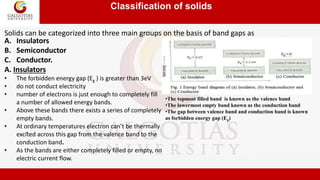
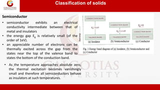
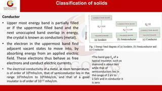
This document provides an overview of the Semiconductor Physics course taught by Dr. Susmita Majumdar. The course will cover topics related to energy bands in solids including the Kronig-Penney model, Bloch's theorem, and band theory. It will explain how these concepts are used to classify materials as insulators, semiconductors, or conductors based on their band gap. The objectives are to apply the Kronig-Penney model to 1D periodic potentials and use band theory to classify different types of solids. Prerequisites include knowledge of the Schrodinger equation and energy levels in a 1D potential box. Practice questions are provided to help students understand how band structure varies


![Prerequisite/Recapitulations
Course Code : BBS01T10
--
2
2
2
8mL
n
h
En
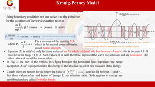
2. The allowed energy for 1D potential box,
The potential energy within the
1D crystal or box is
V(x) = 0 for o < x < L
V(x) = for x 0 and x L
where m is mass of particle, L is the length of potential box and n are
positive integers like 1, 2, 3, 4, 5....
2
0
)
(
)]
(
[
2
)
(
2
2
2
h
with
x
x
V
E
m
dx
x
d
1. Schrödinger equation in one dimension is
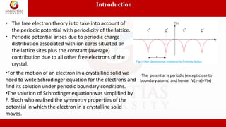
3. Bloch’s Theorem
• This is a mathematical representation regarding the form of one
electron wave function for a perfectly periodic potential function
with a period a.
• According to Bloch's theorem, the wave function solution of the
Schrödinger equation when the potential is periodic, V(x+a)=V(x) can
be written as:
Where u(x) is a periodic function which satisfies:](https://image.slidesharecdn.com/l-1-220930154251-0cb872ea/85/L-1-4-Energy-bands-in-solids-pptx-5-320.jpg)
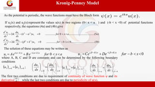
![Energy bands in solids
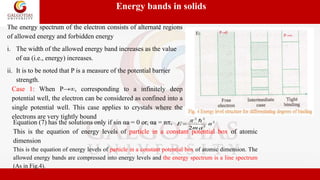
Case 2 : When P→0, corresponds to no barrier,
the electron can be considered to be moving
freely through the potential wells.
2
2
2
k
mE
]
,
2
[
,
2
2
2
2
2
p
h
k
As
m
p
m
k
cos αa=cos ka i.e., α = k or α2 = k2
E= ]
,
2
[
,
2
2
2
2
2
p
h
k
As
m
p
m
k
which is appropriate to the
completely free particle.
Case 3 : Between these two extreme limits, intermediate case,
the position and the width of the allowed and forbidden
bands for any value of P are obtained by drawing vertical
lines in Fig. 5, the shaded areas corresponds to the allowed
bands (Fig. 4 and Fig.5). Thus by varying P from zero to
infinity we cover the whole range, from the completely free
electron to the completely bound electron.](https://image.slidesharecdn.com/l-1-220930154251-0cb872ea/85/L-1-4-Energy-bands-in-solids-pptx-11-320.jpg)