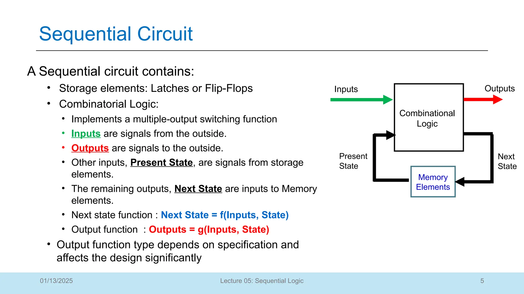
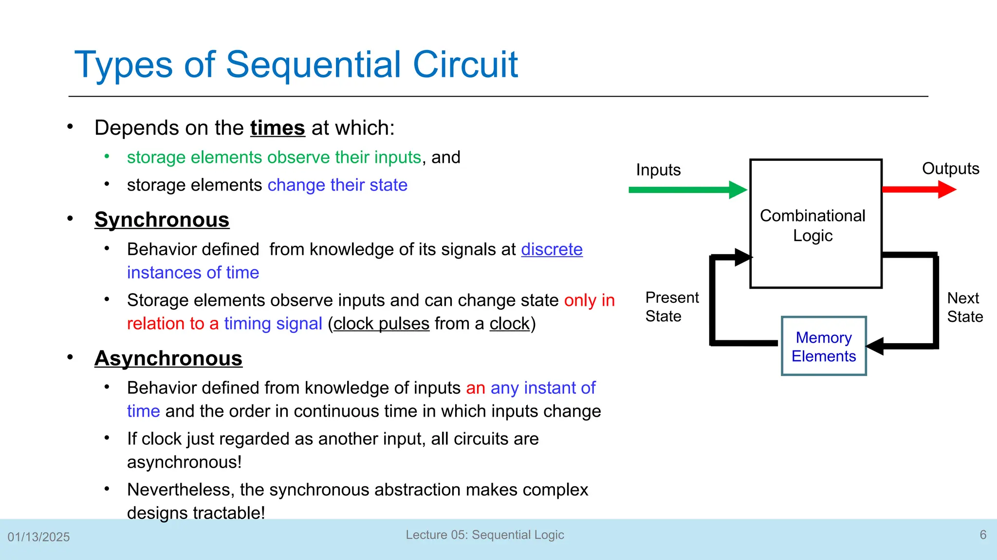
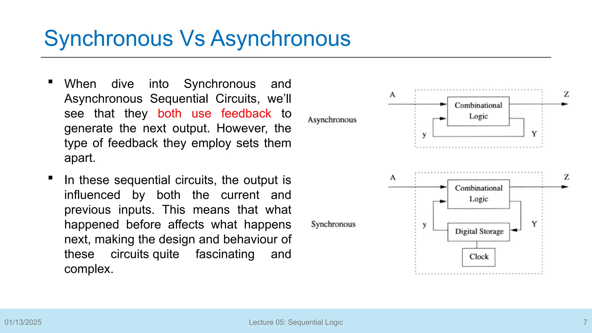
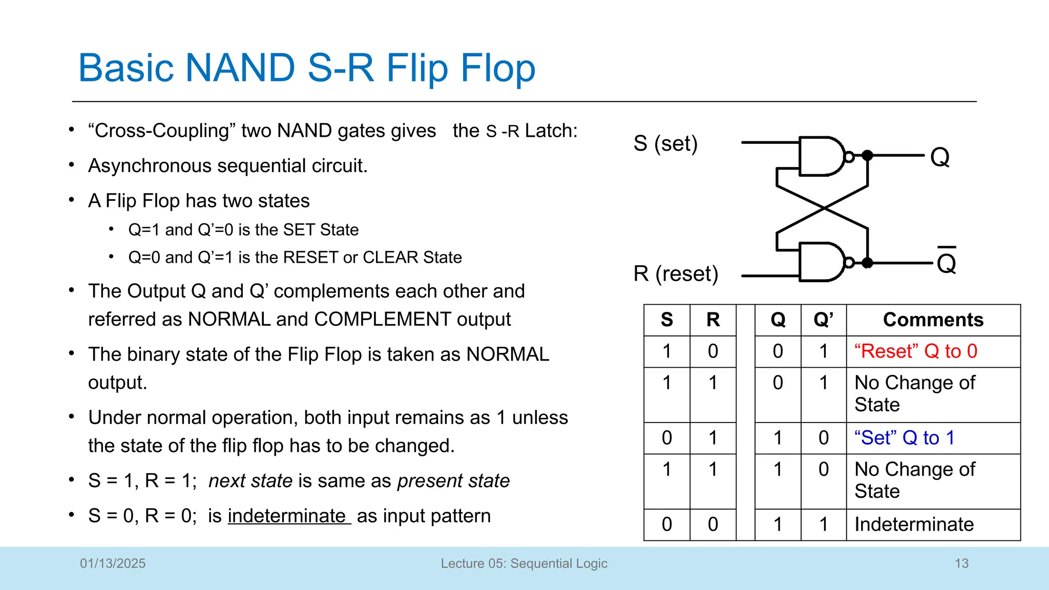
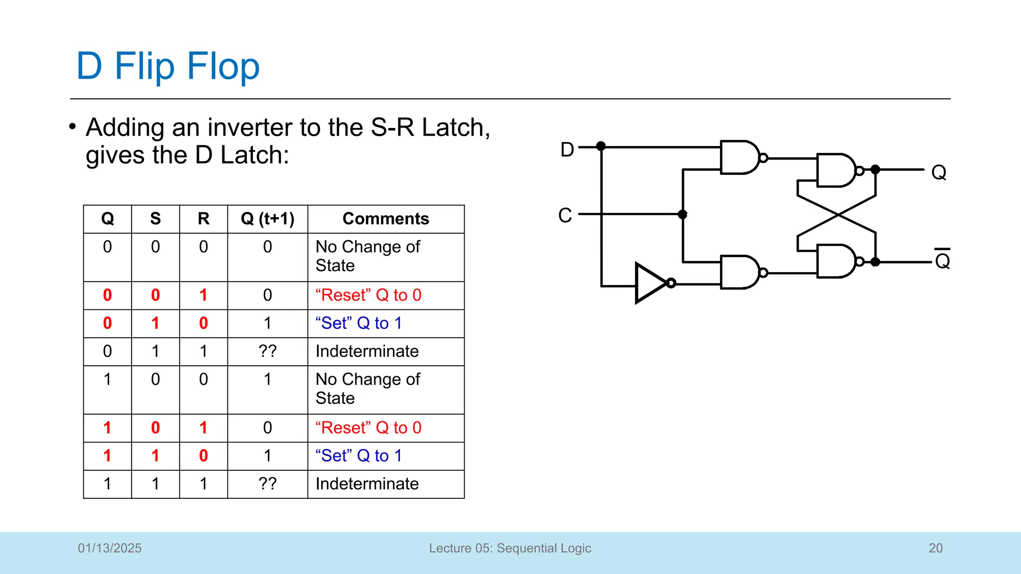
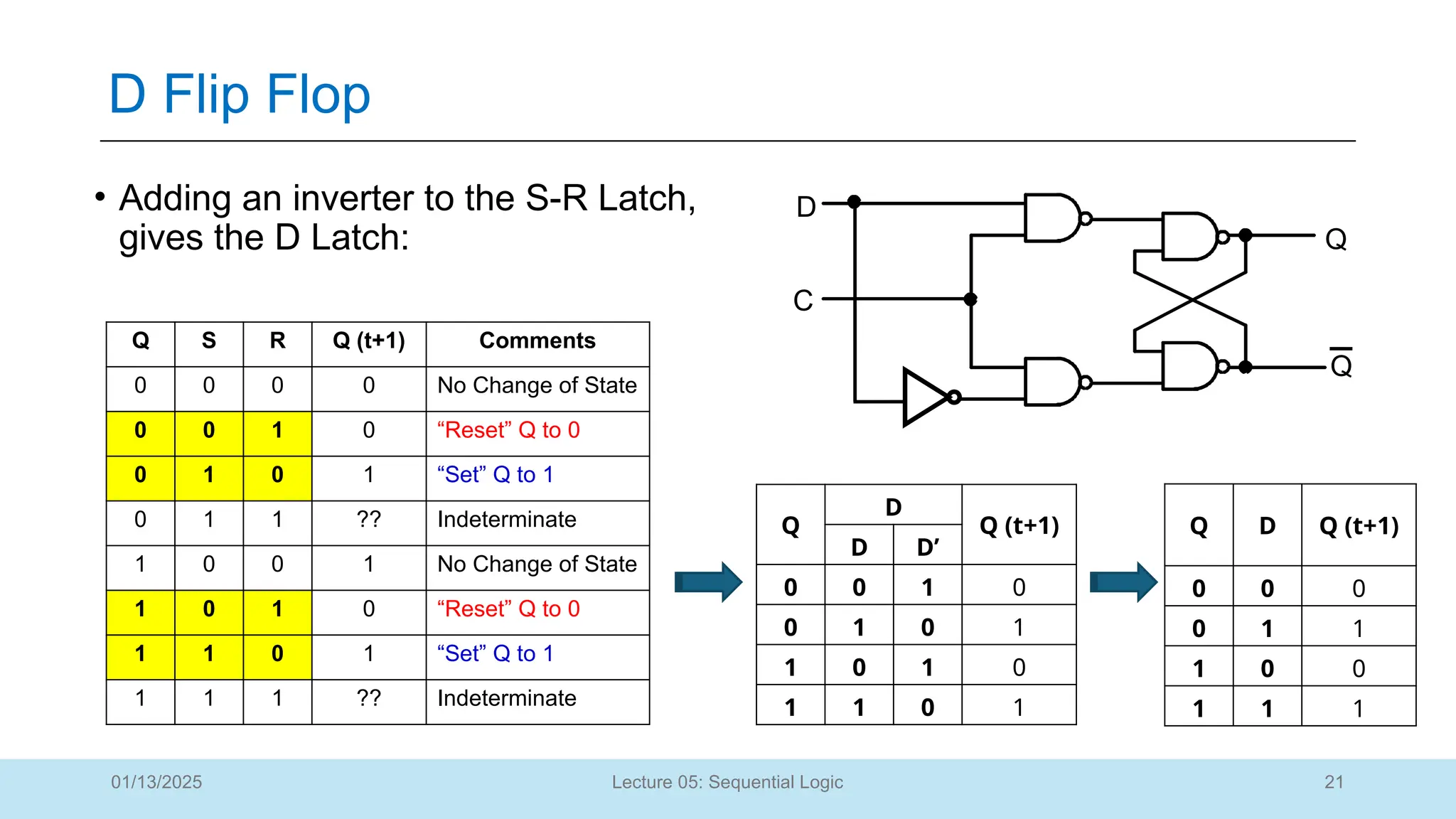
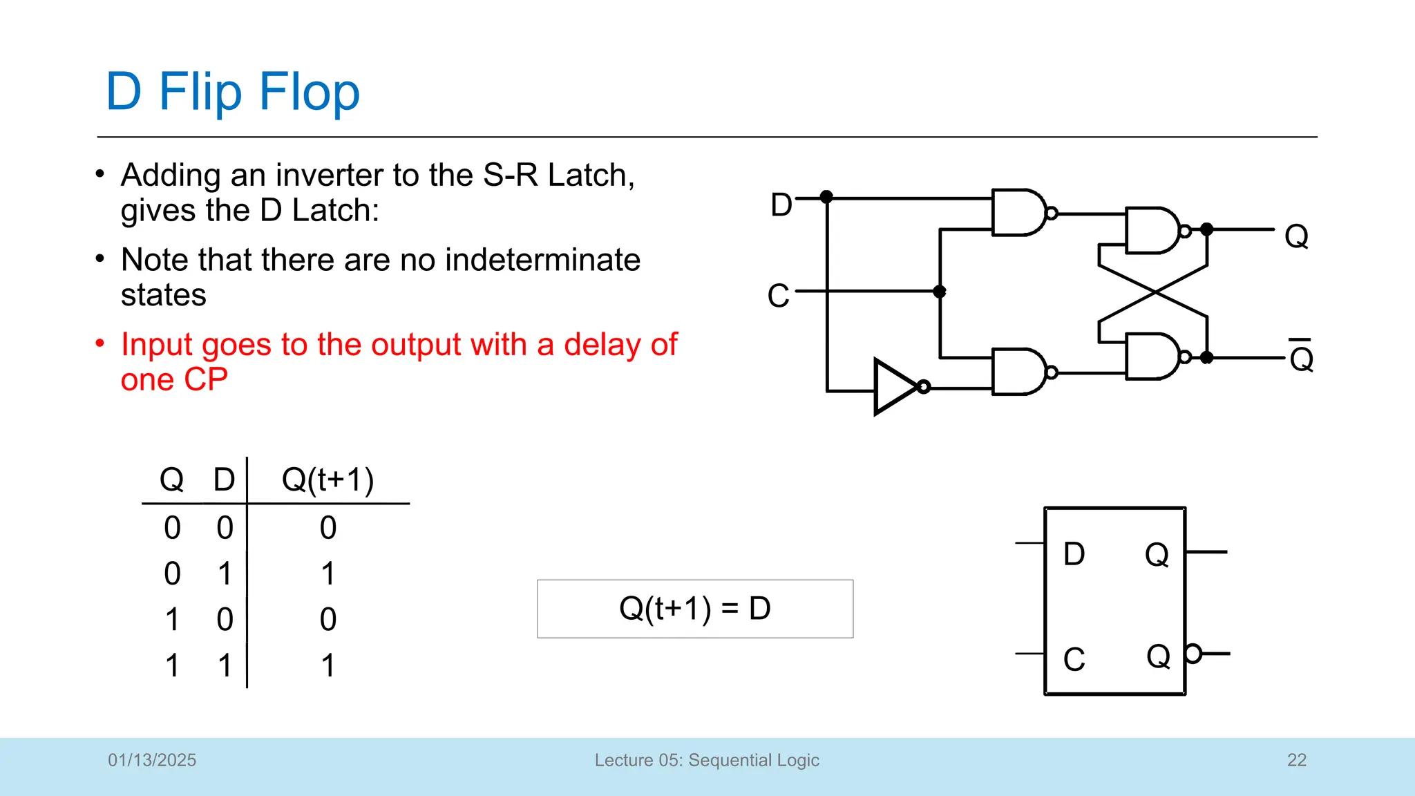
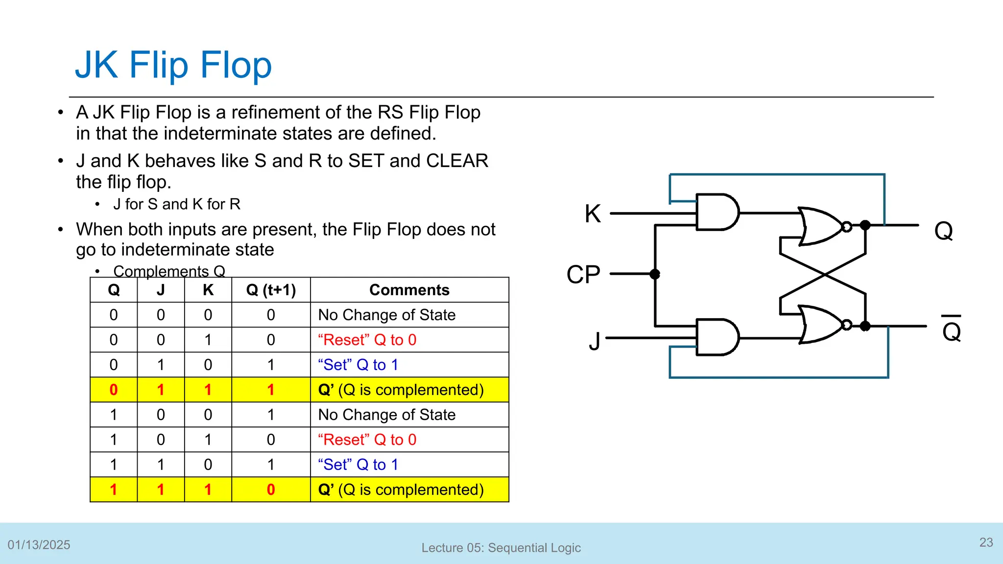
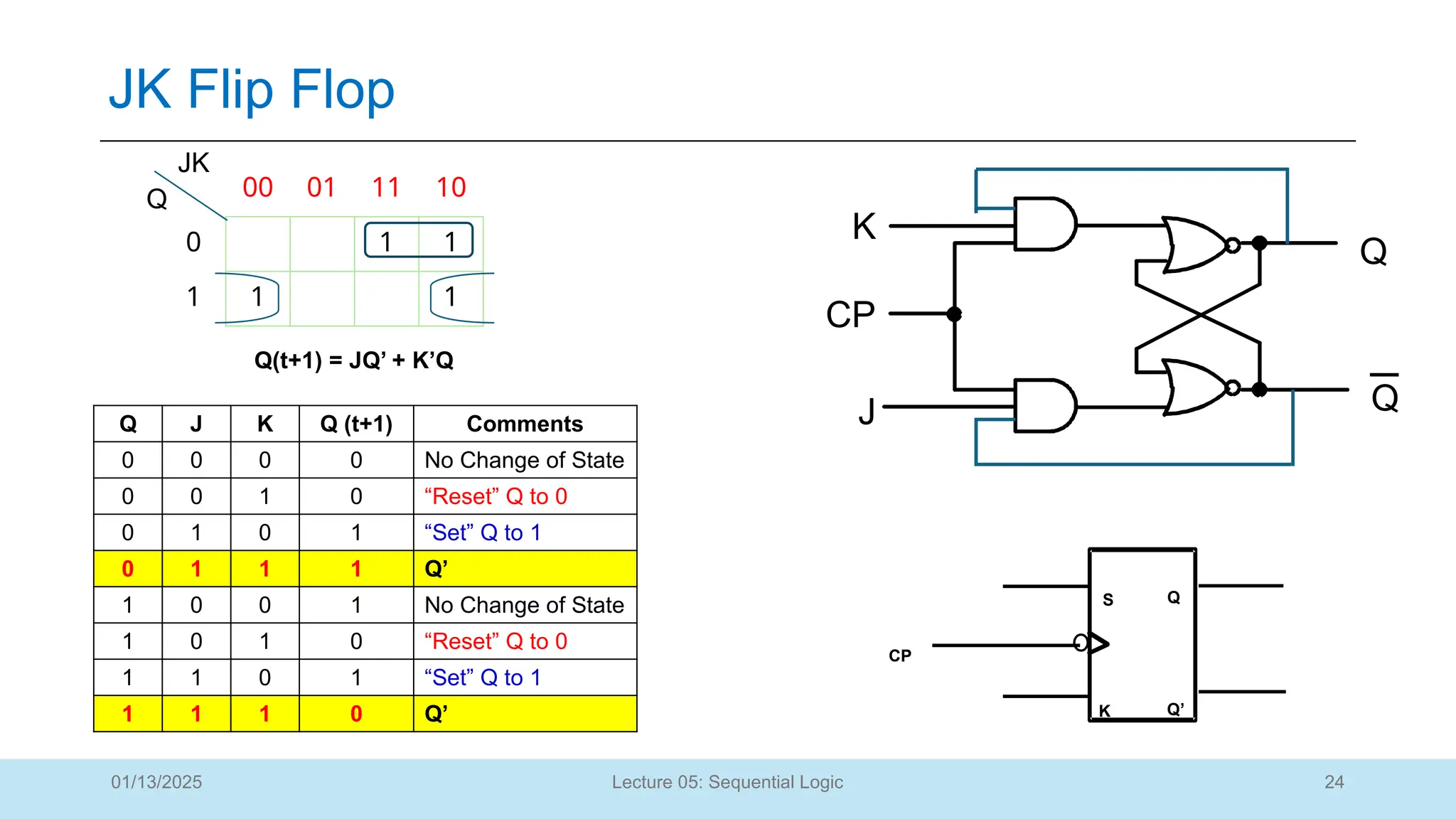
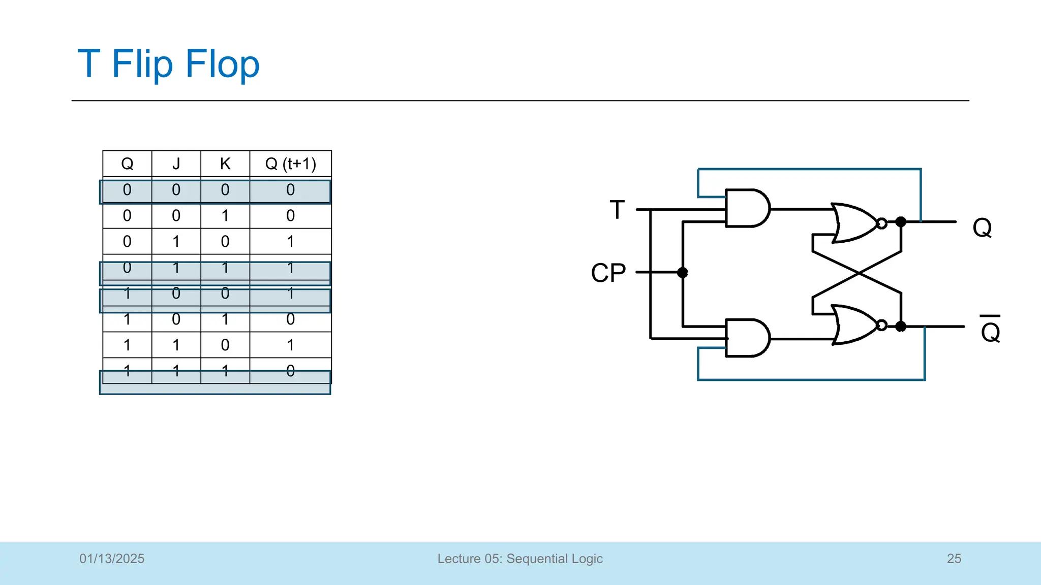
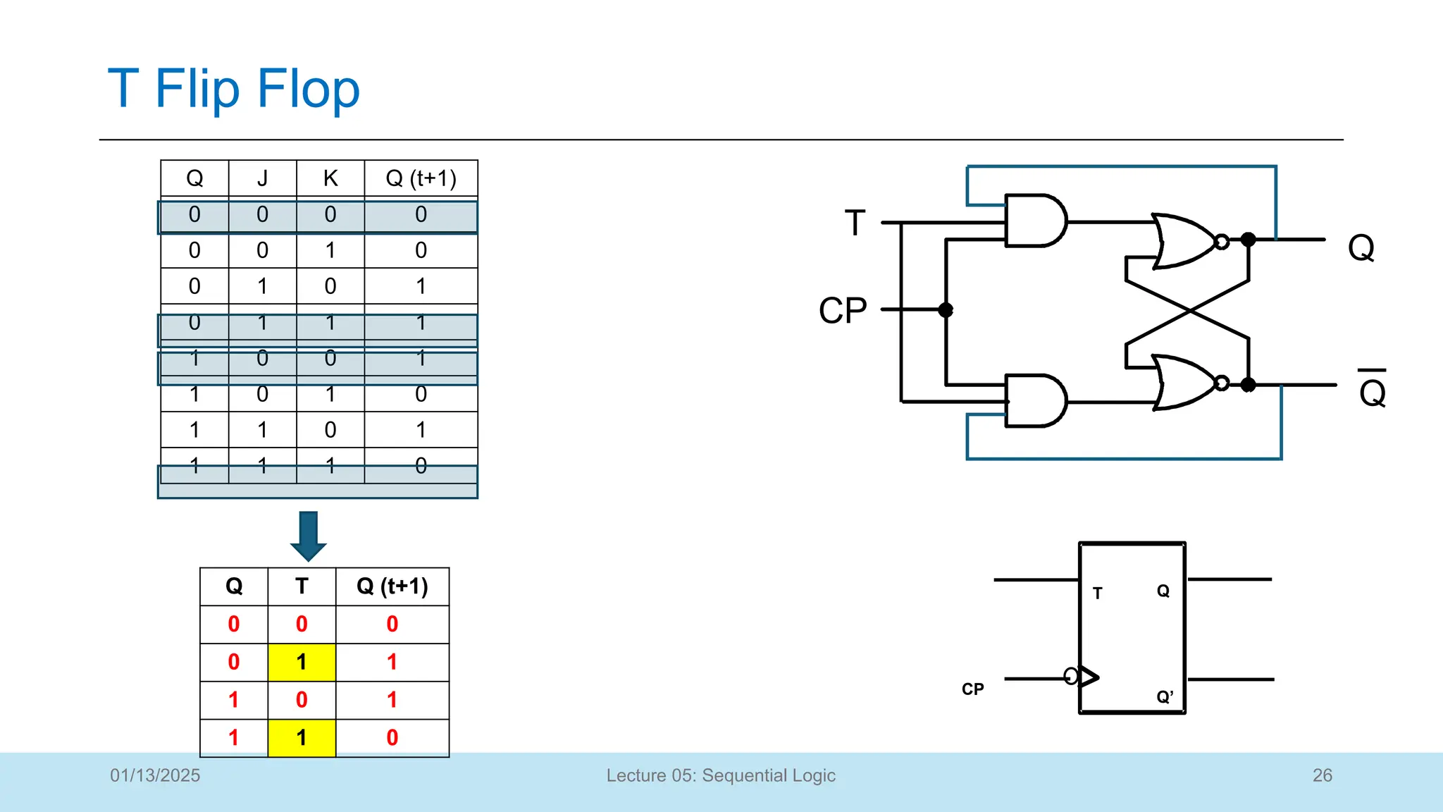
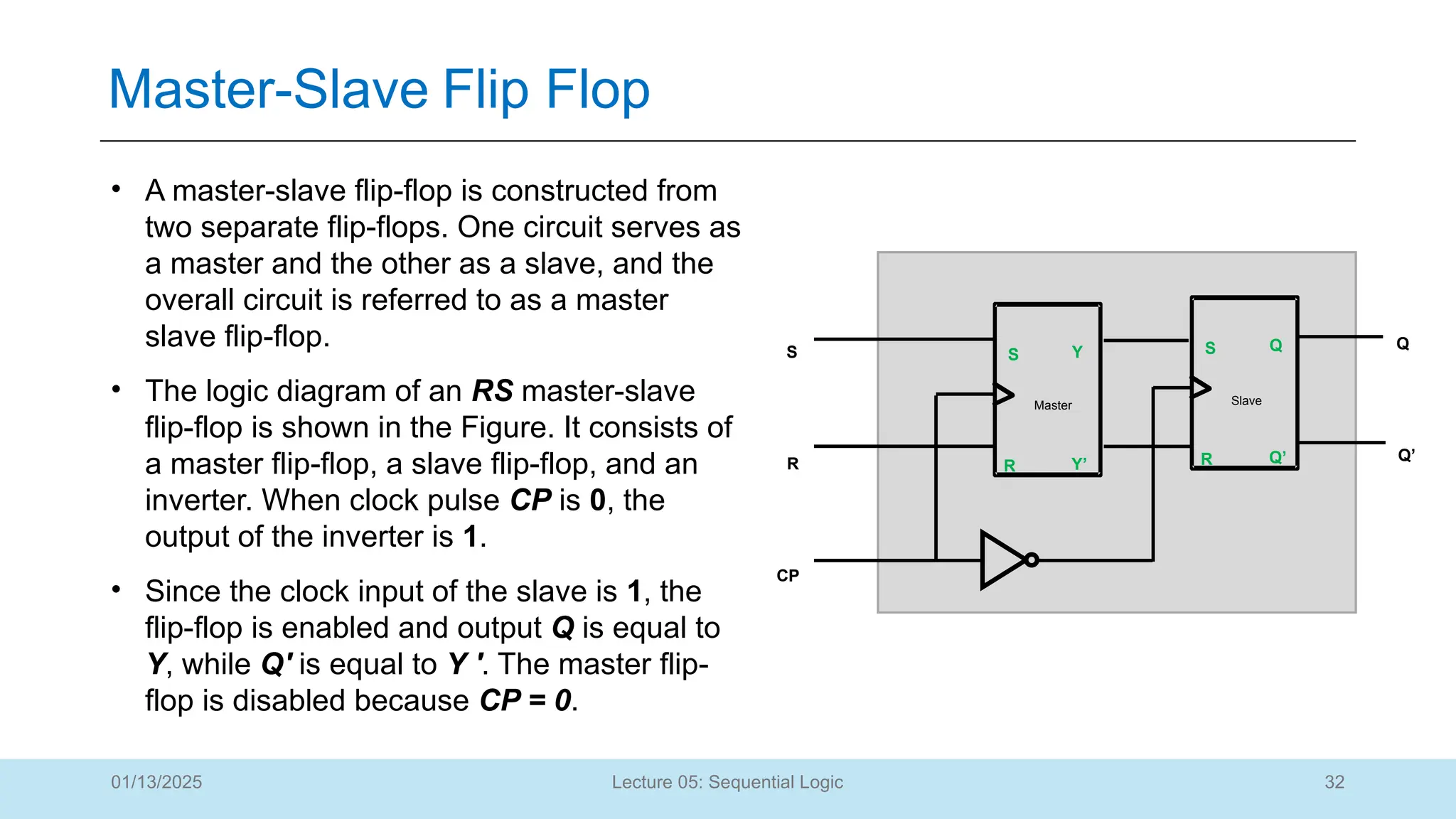
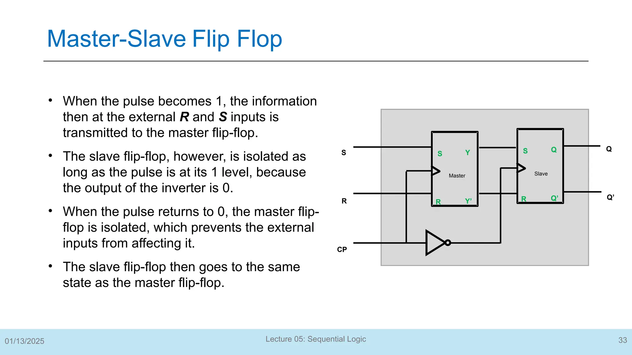
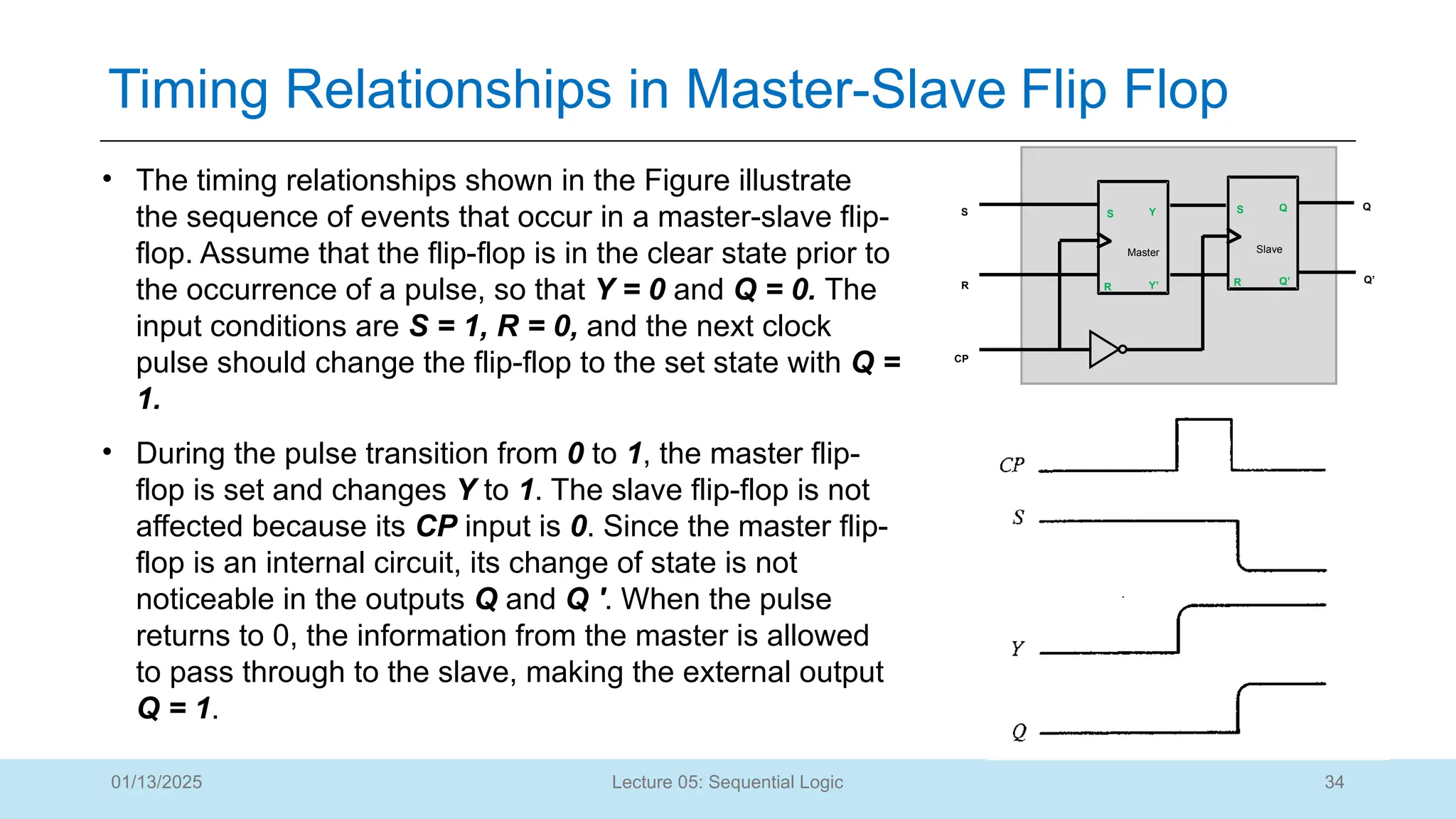
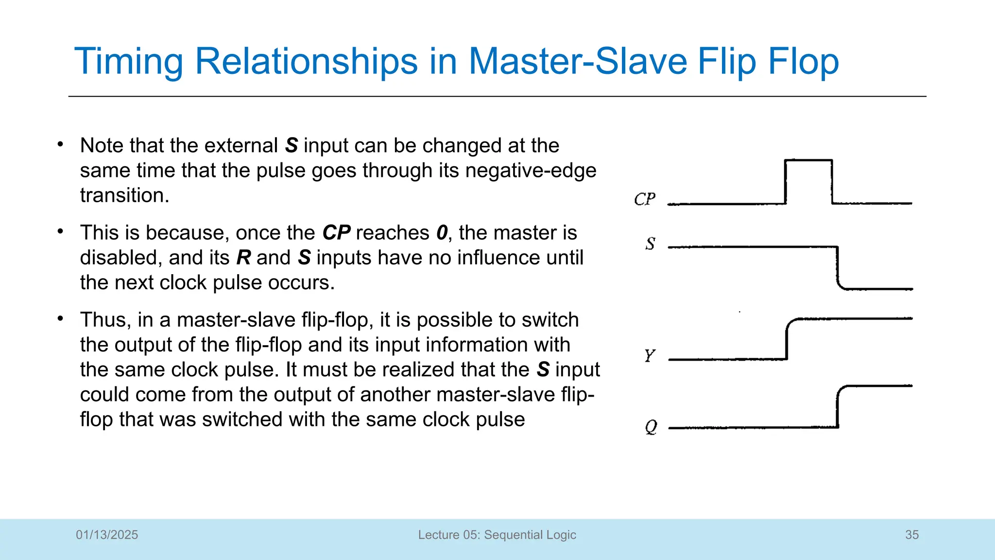
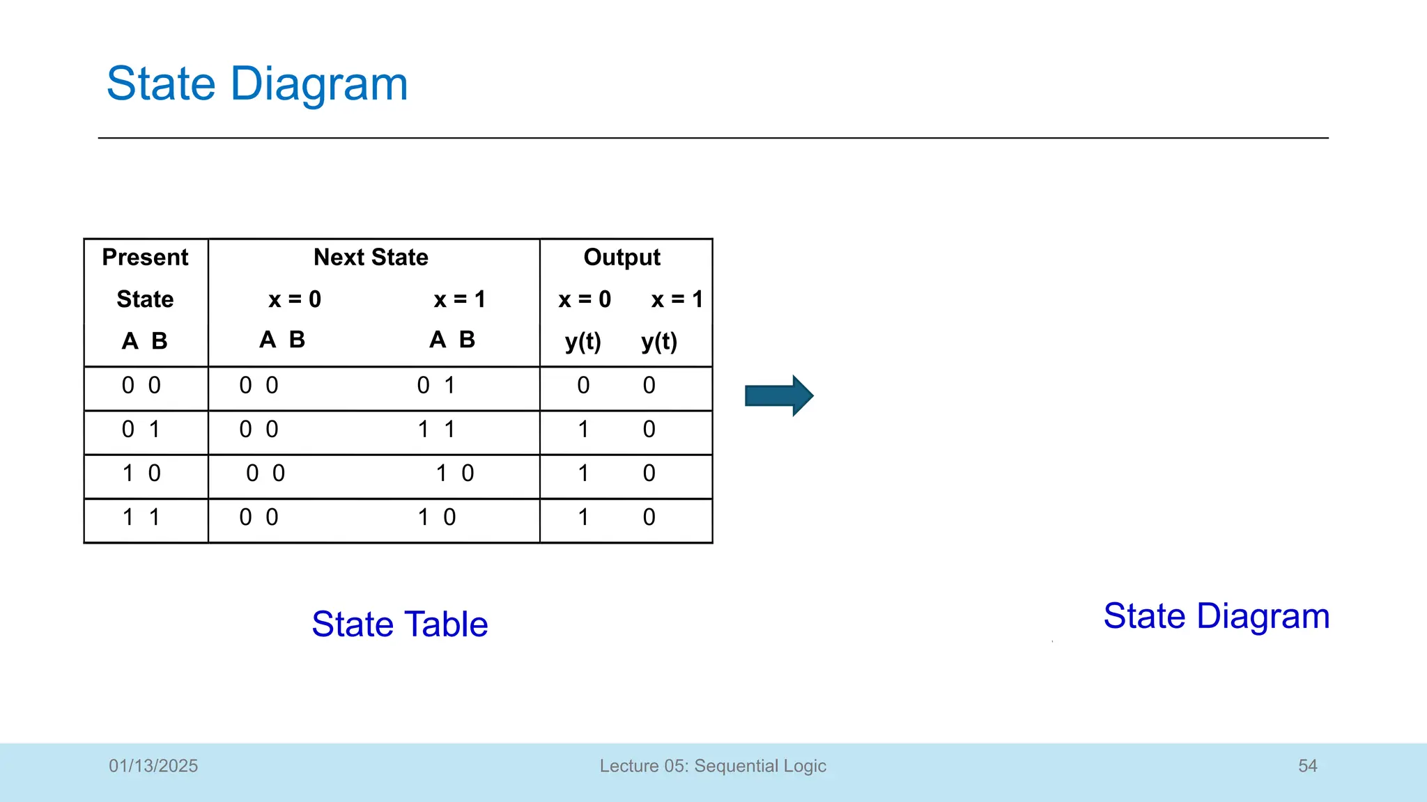
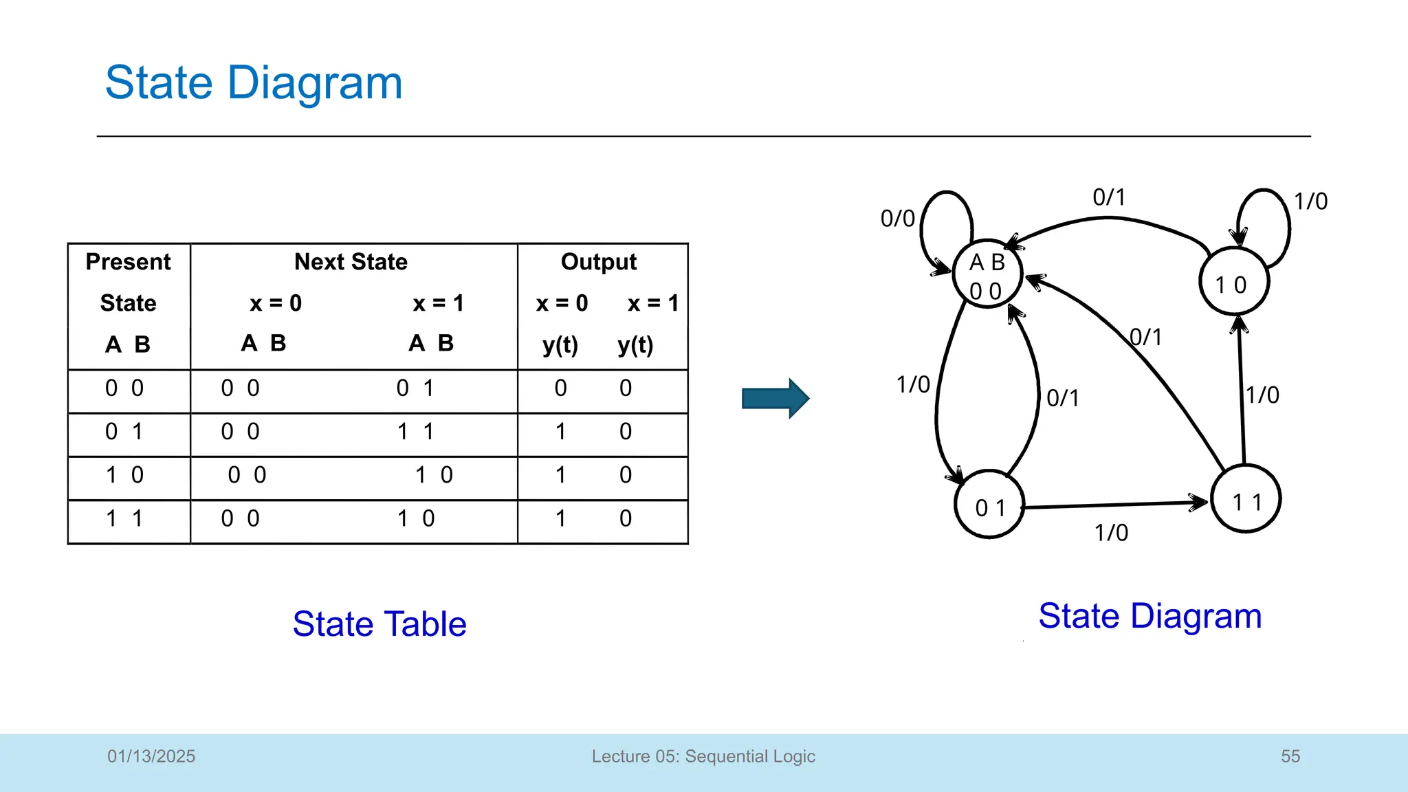
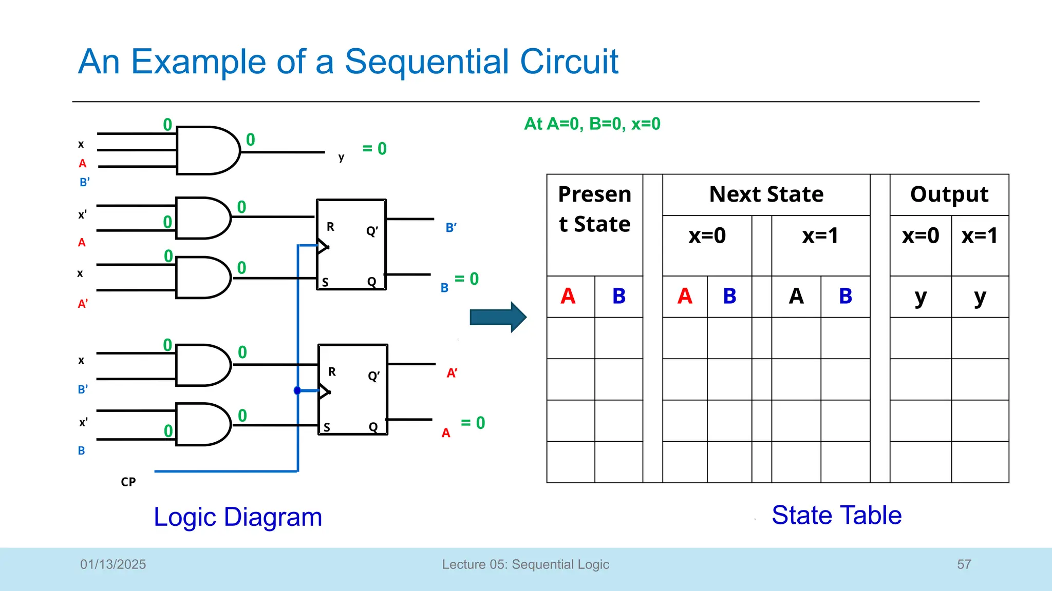
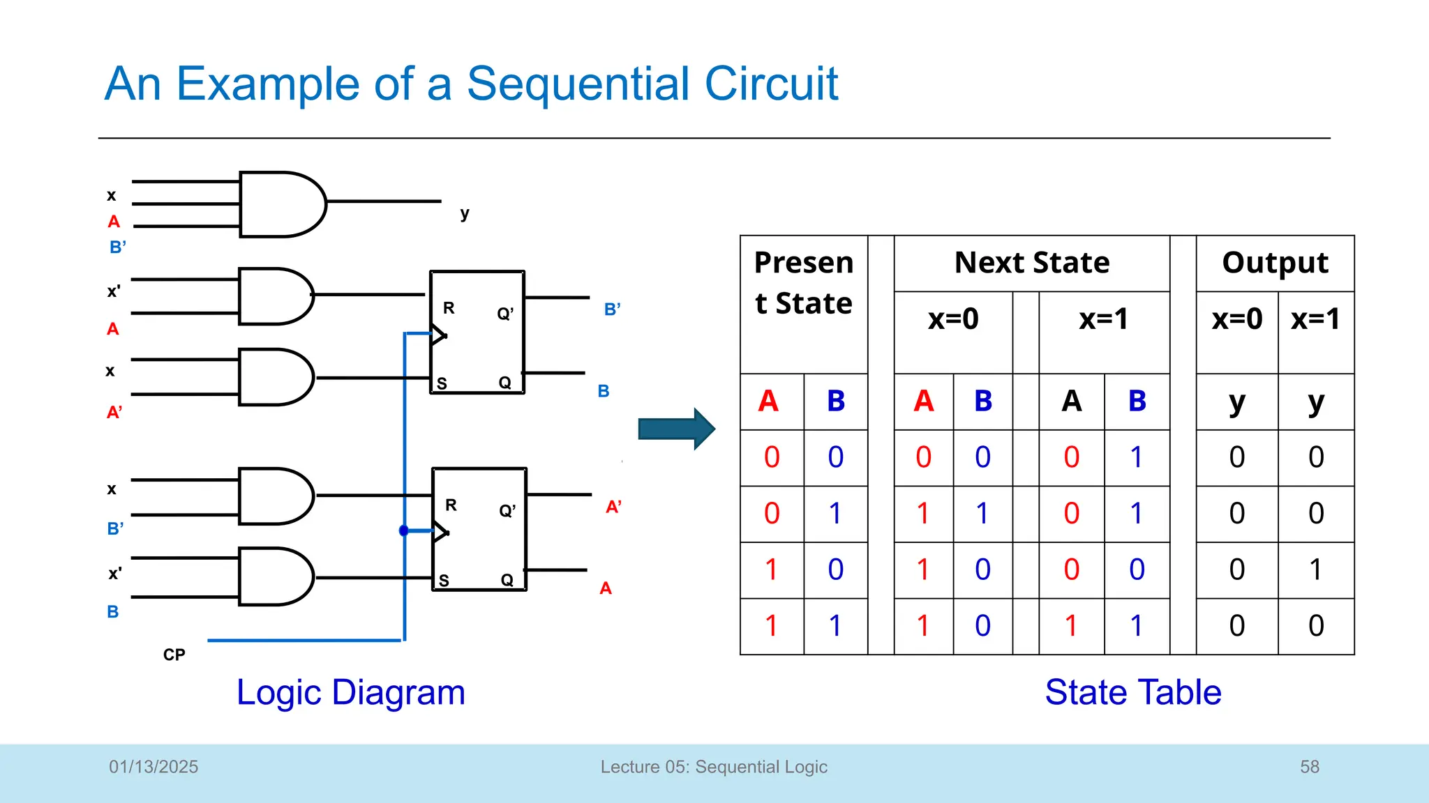
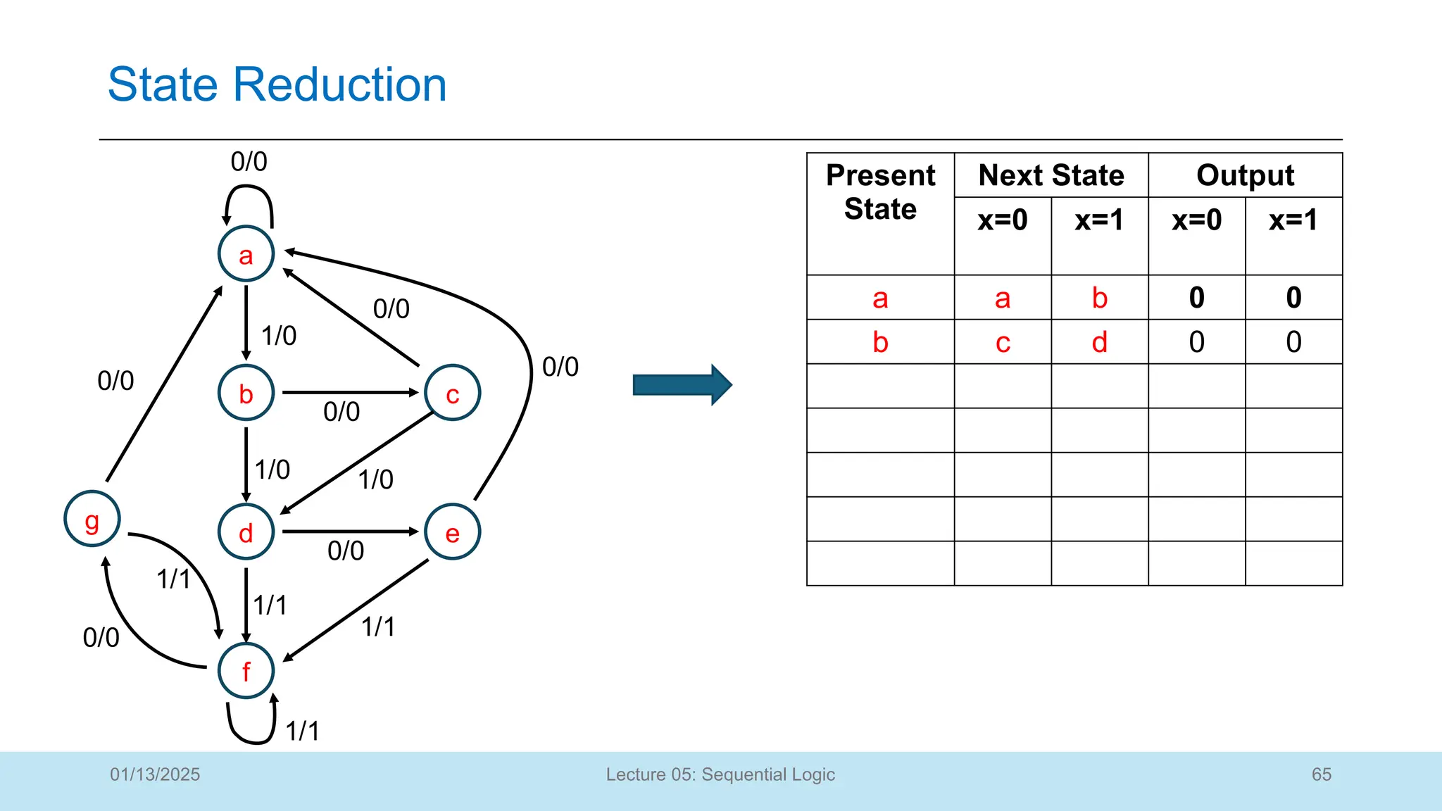
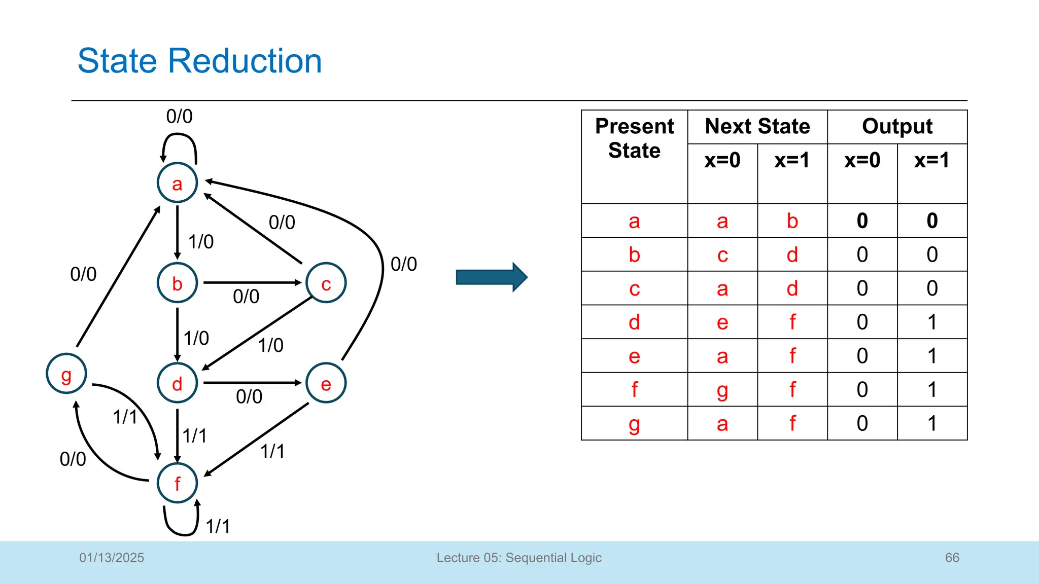
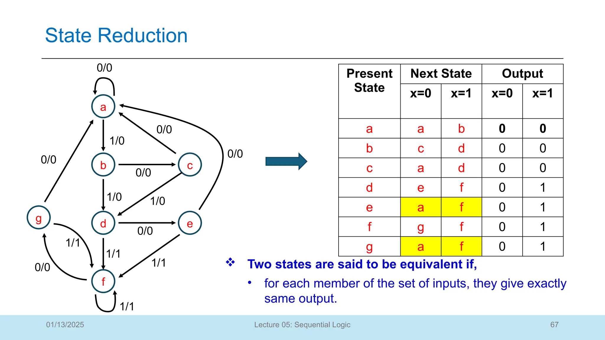
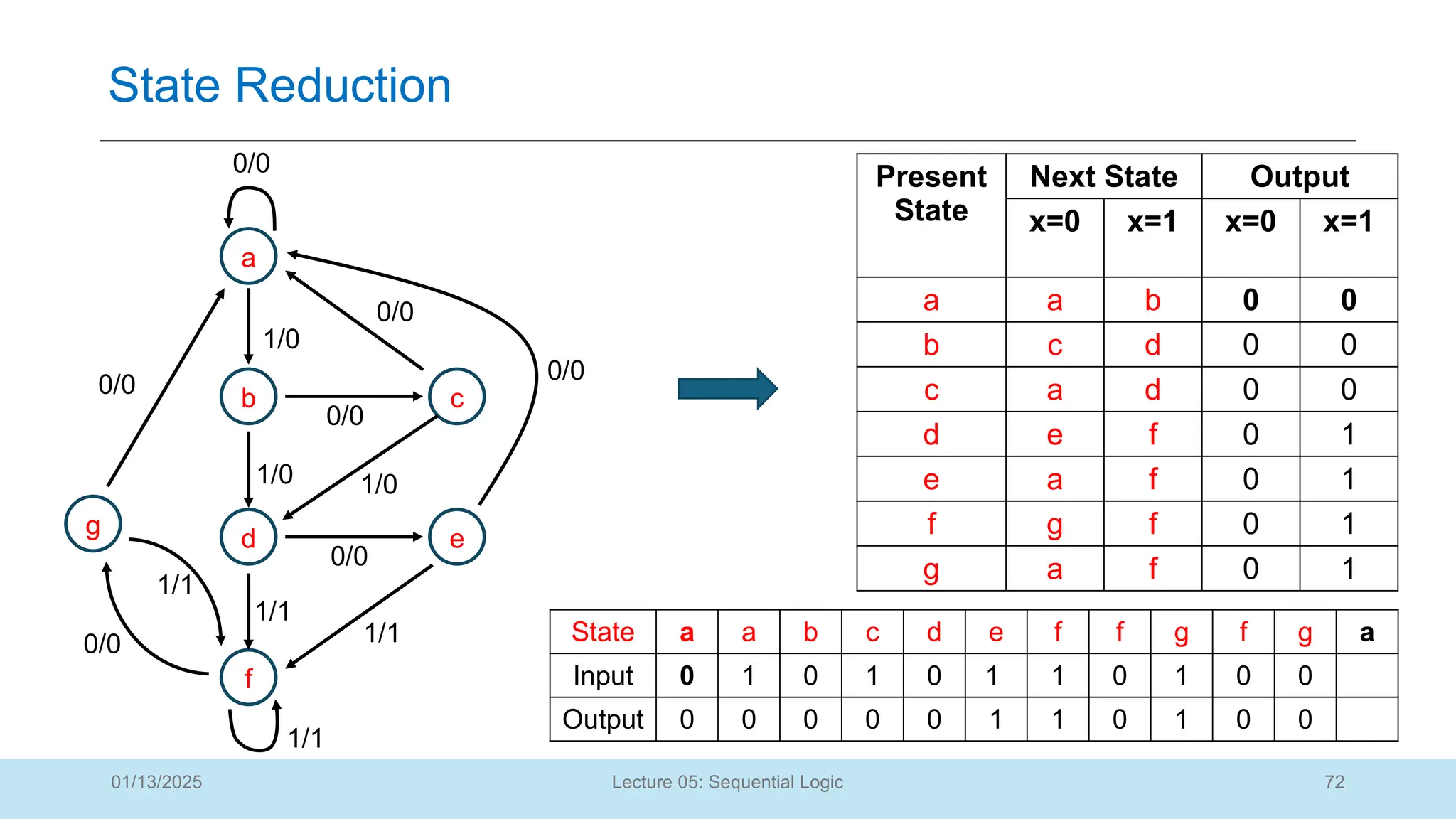
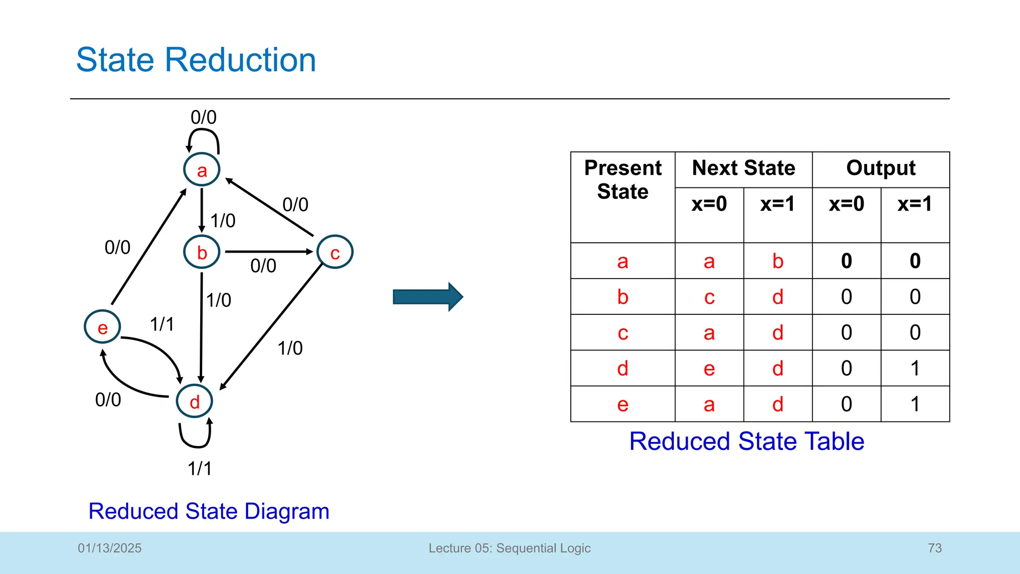
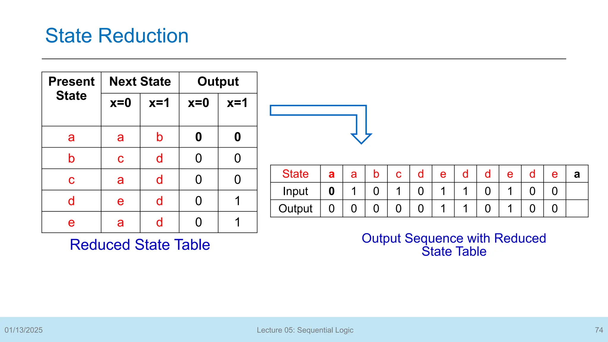
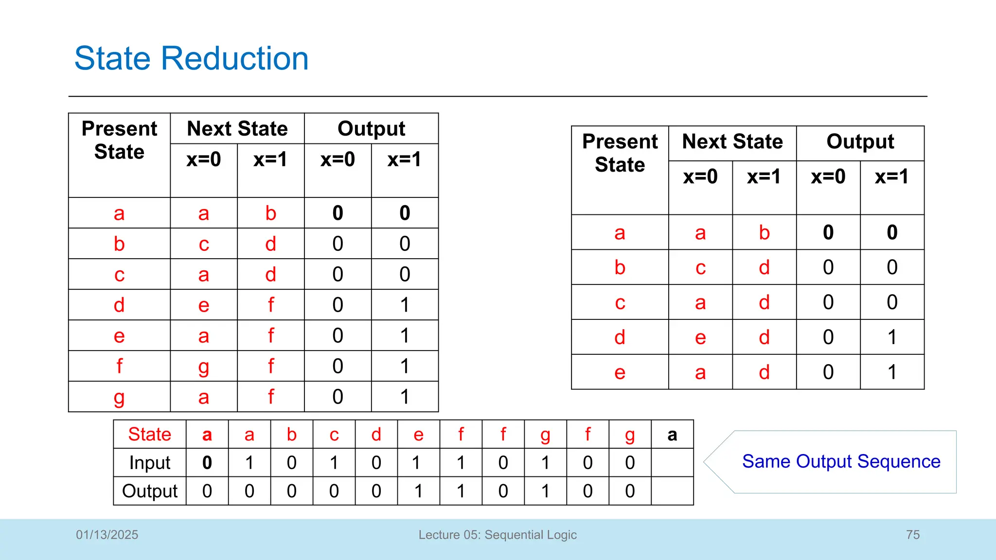
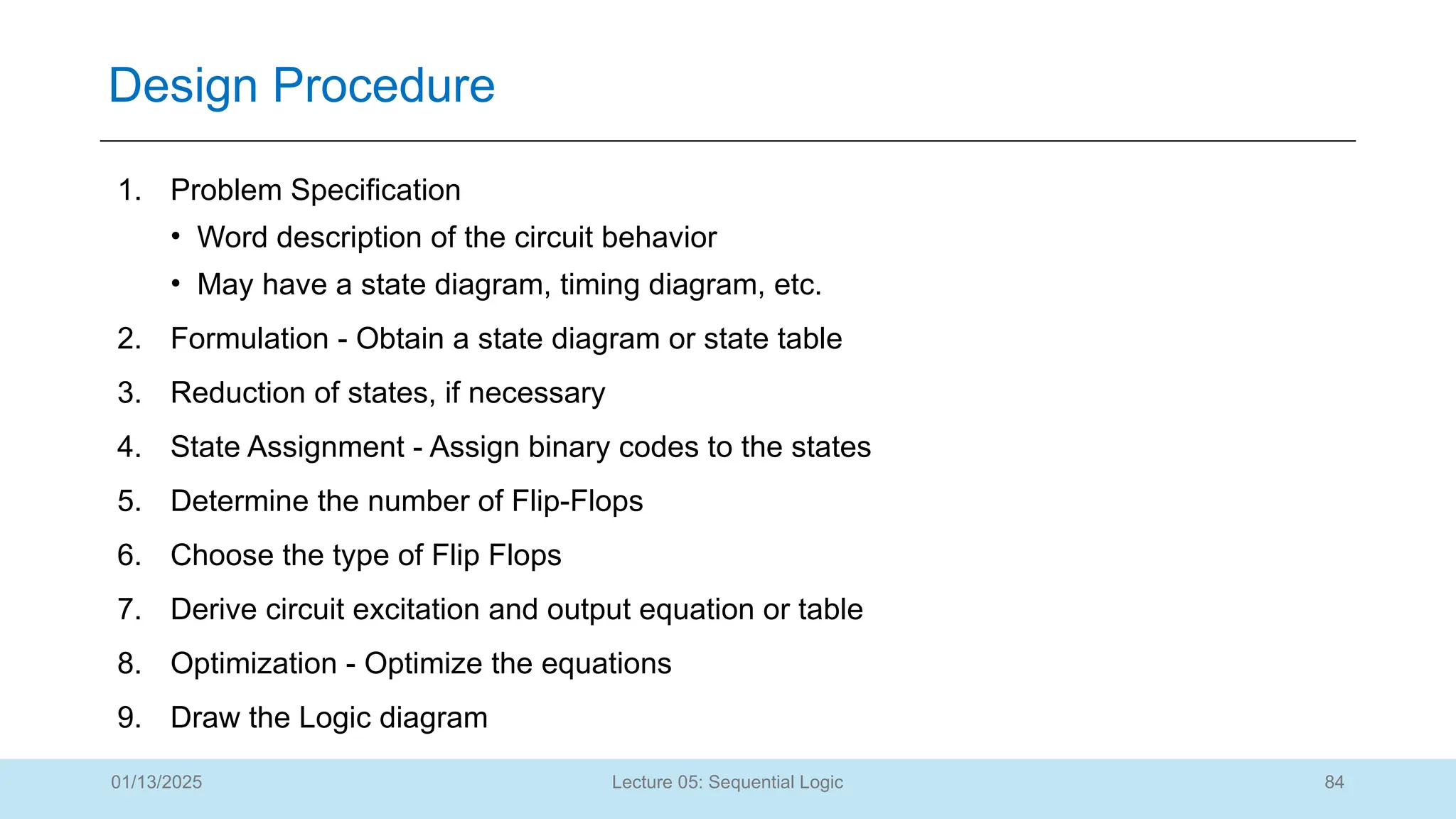
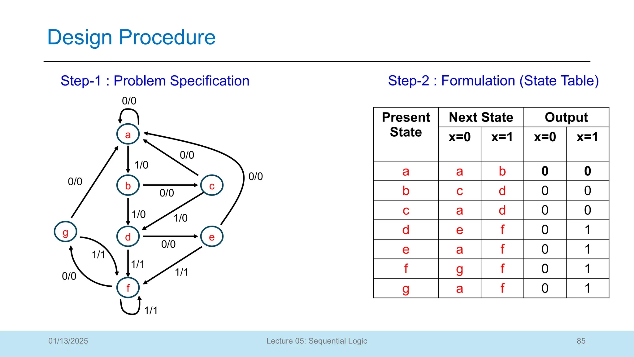
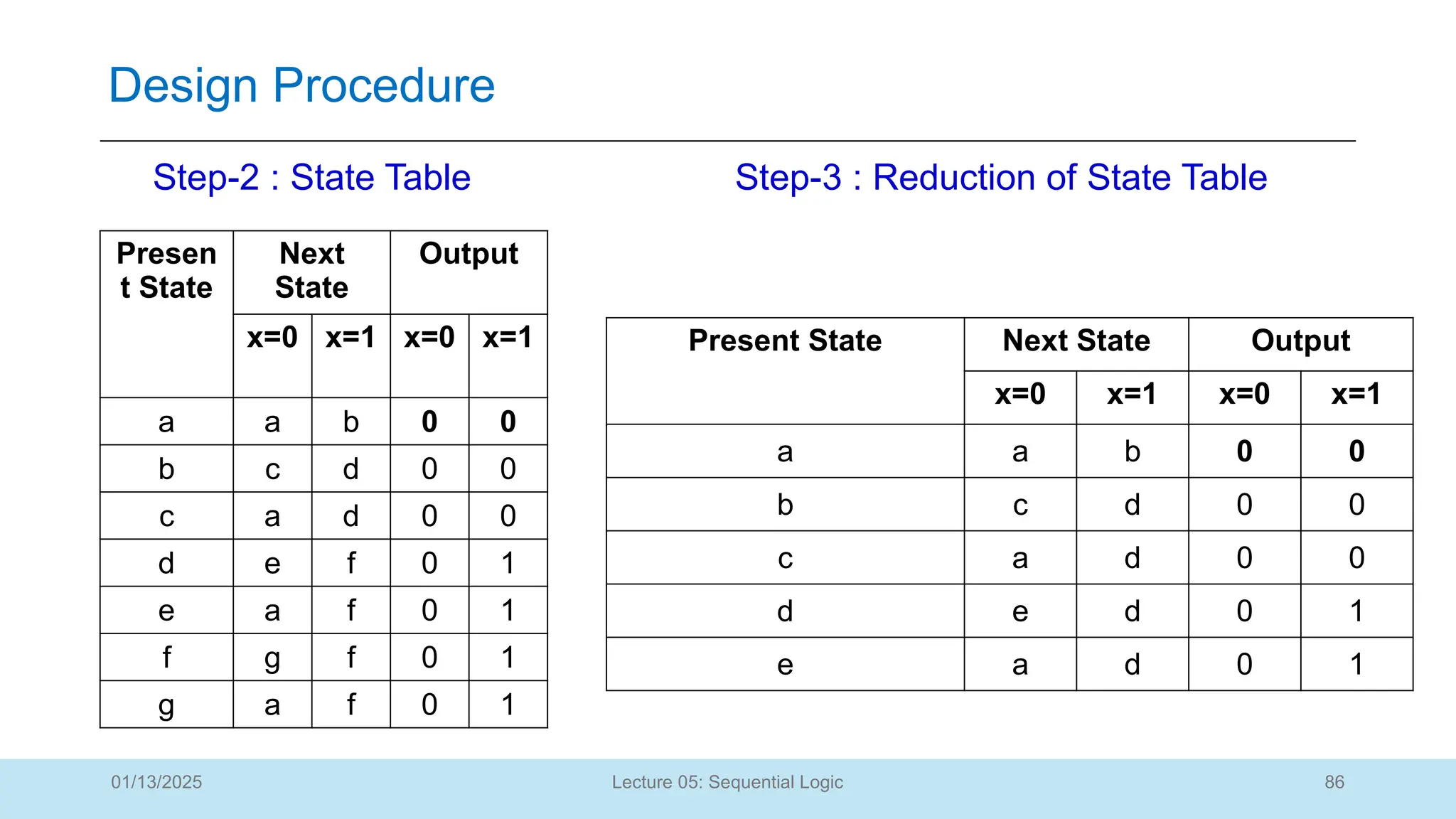
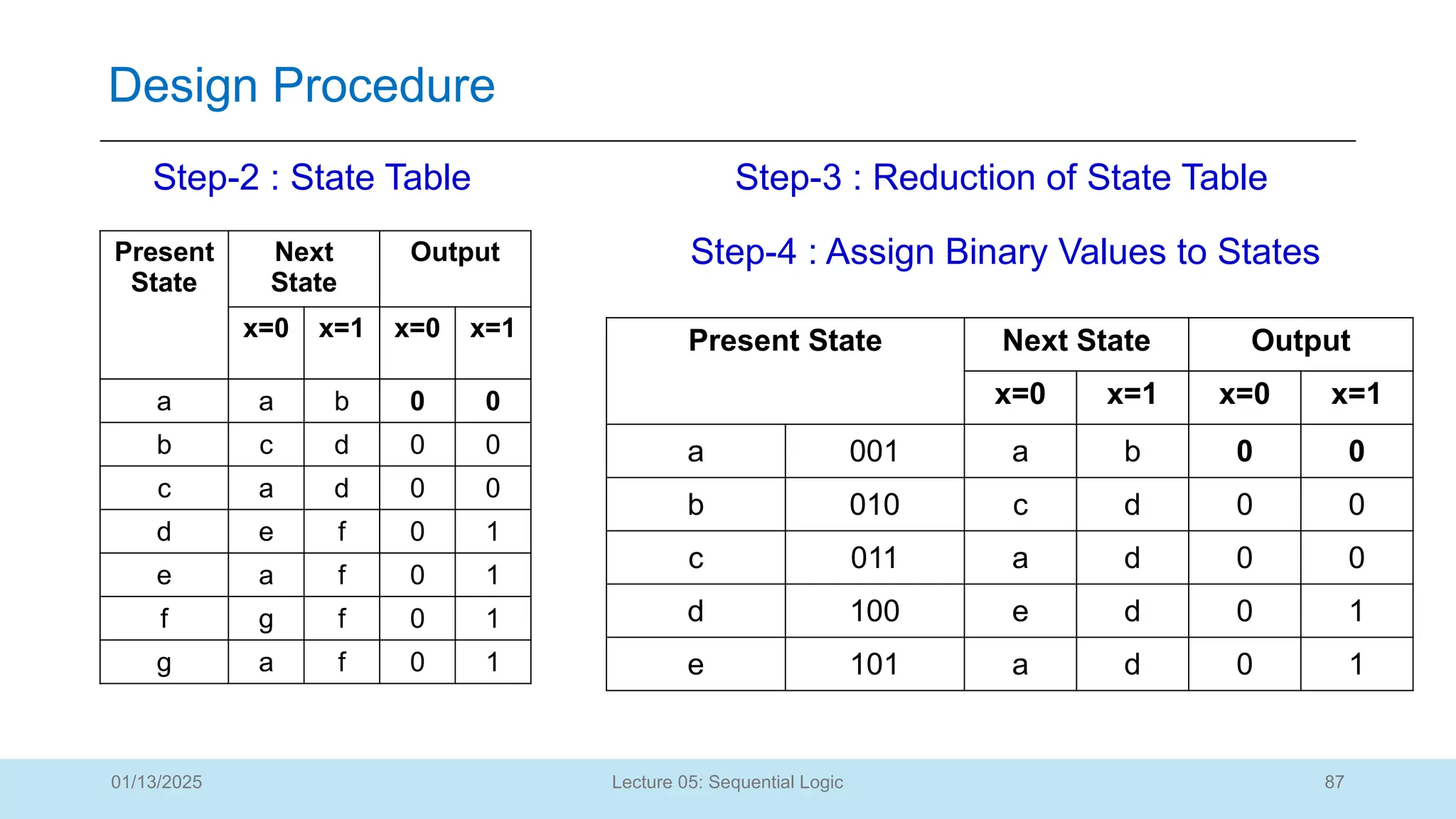
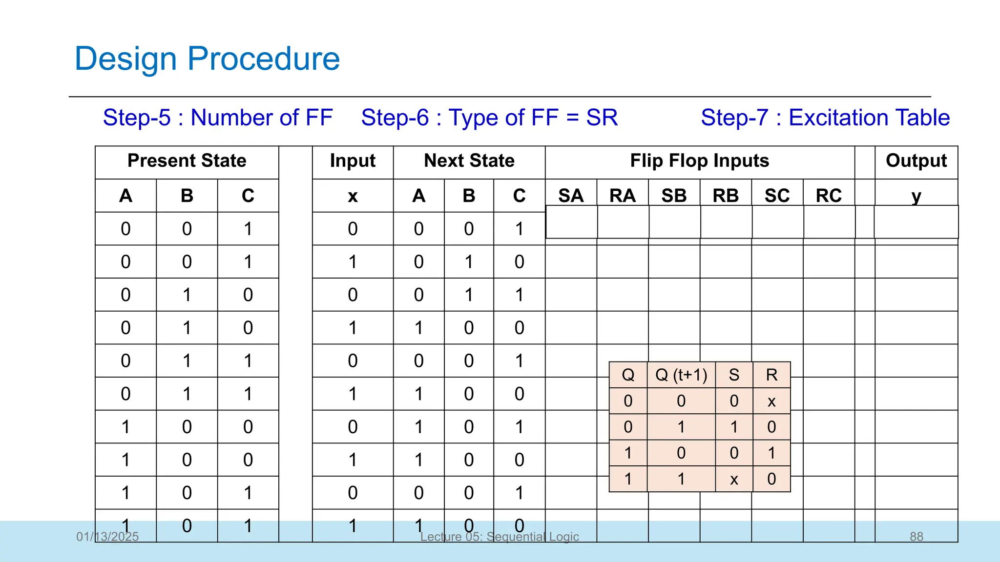
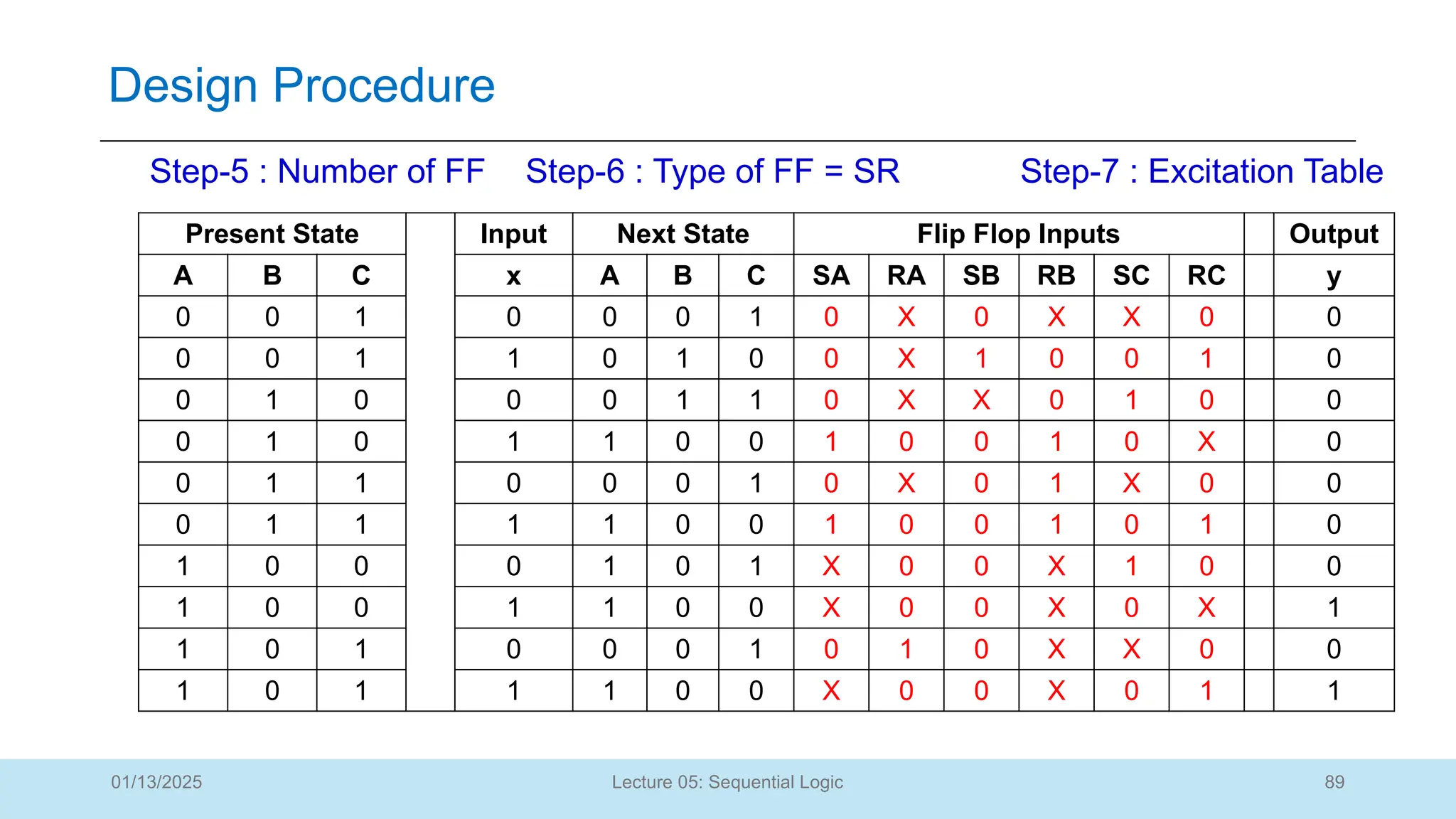
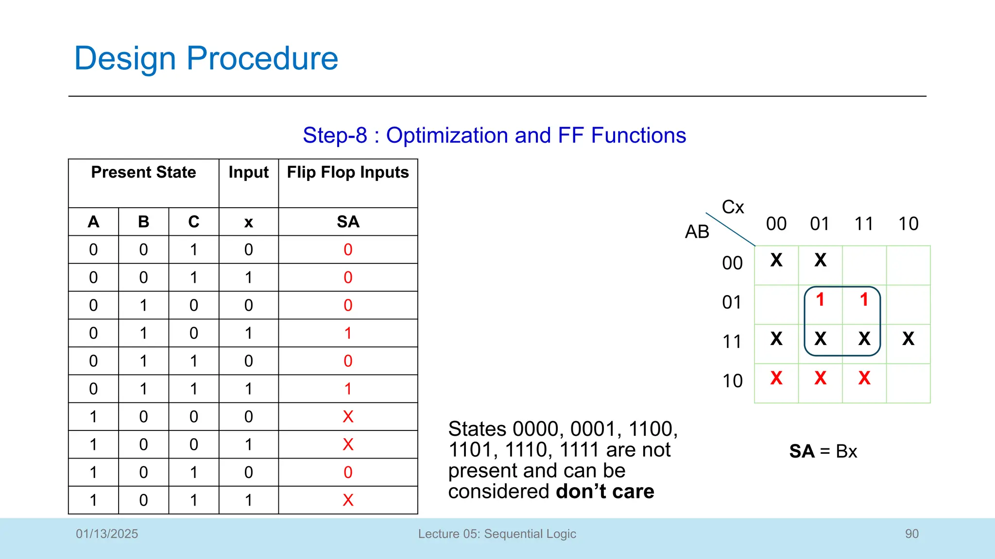
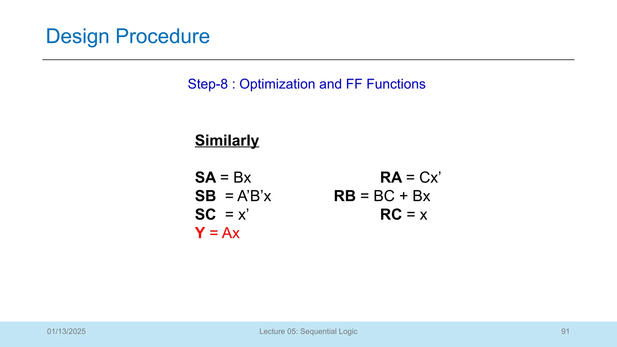
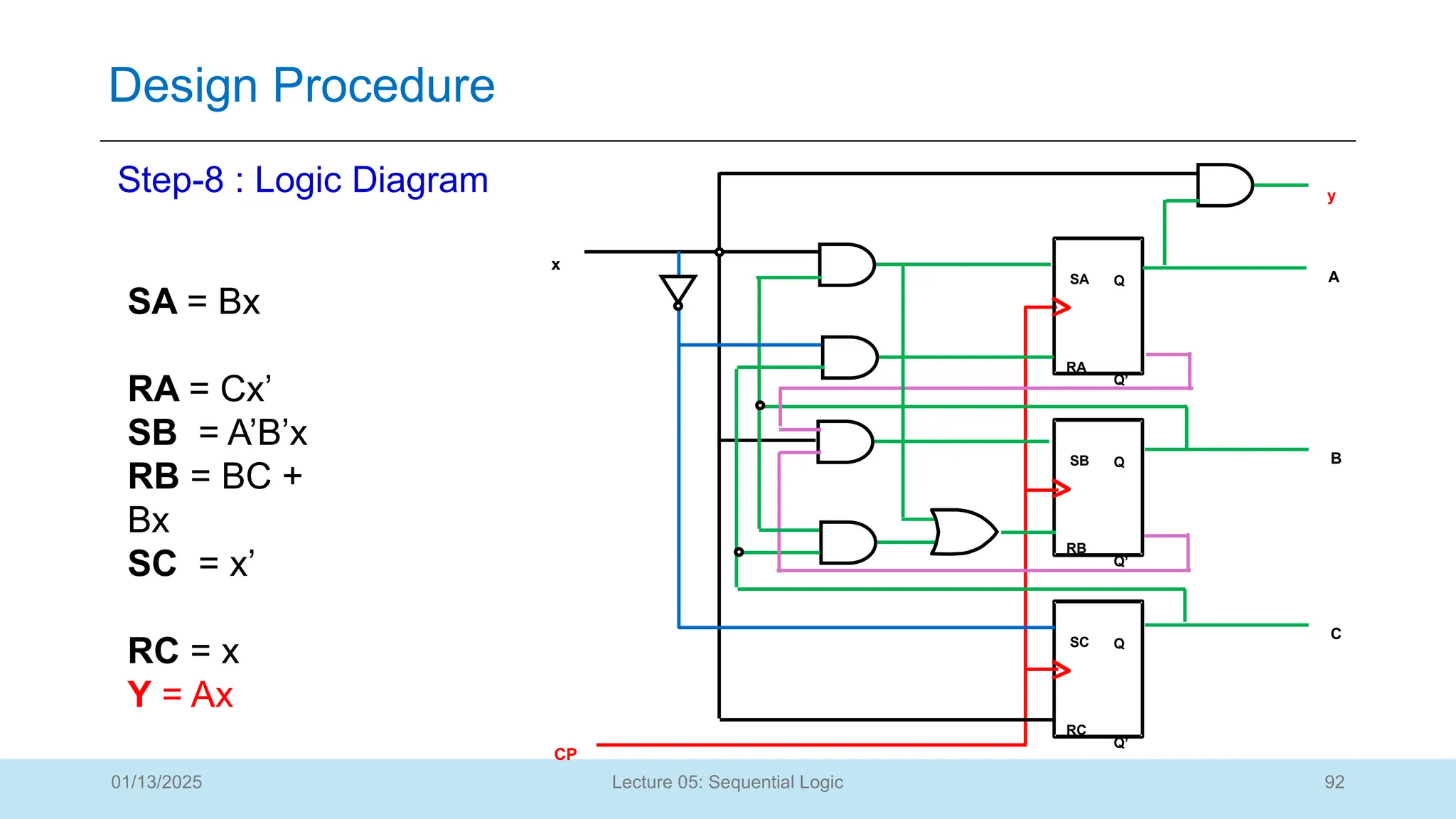
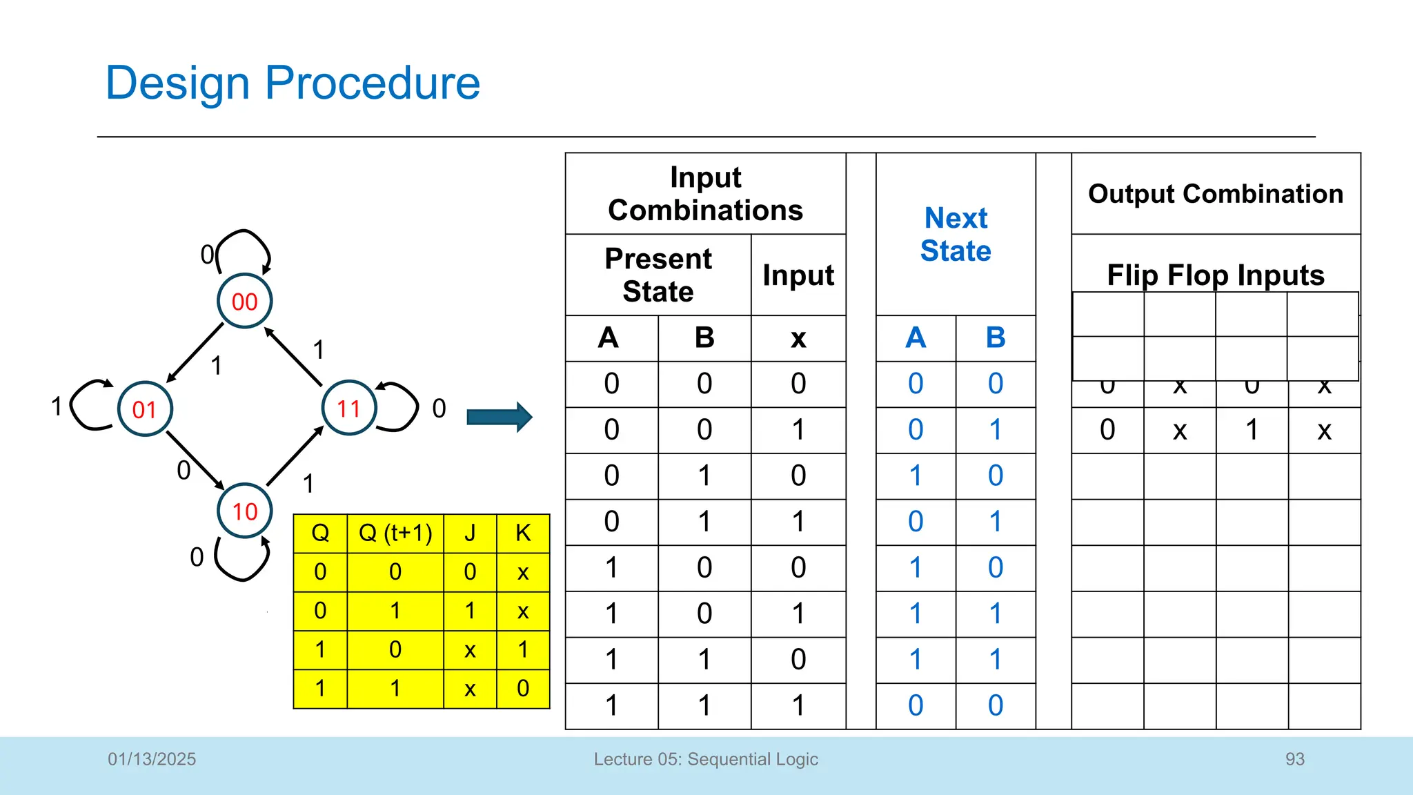
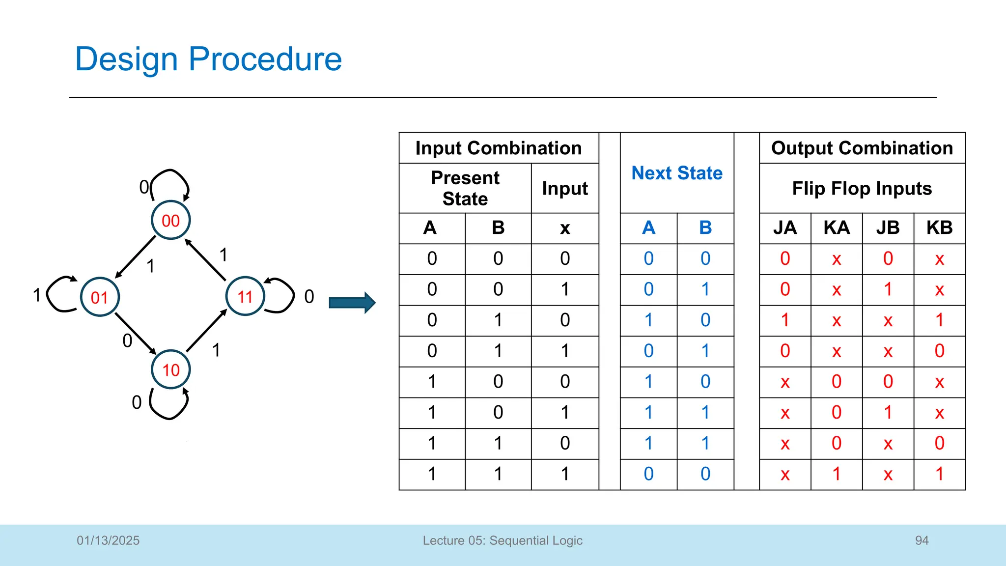
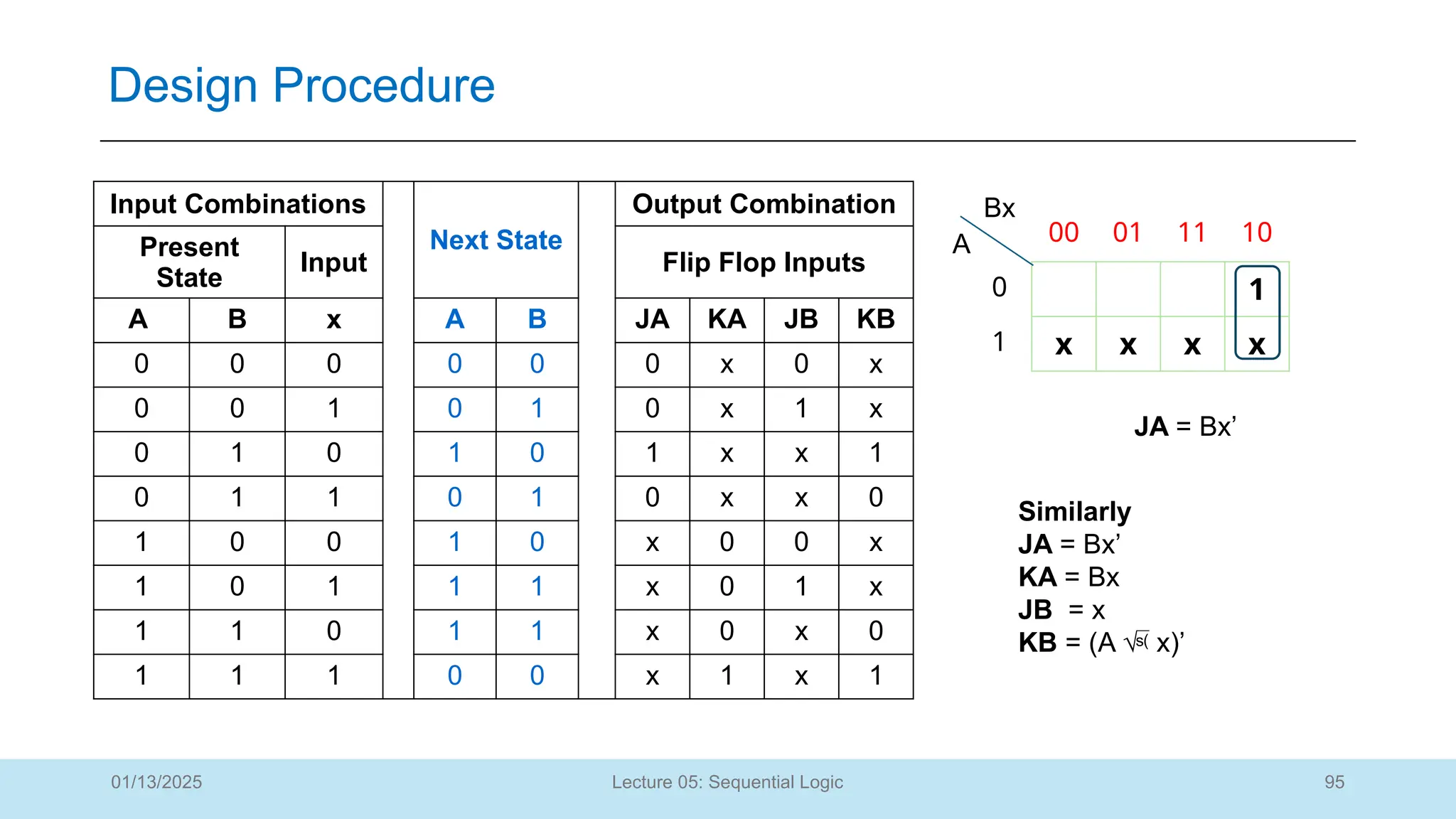
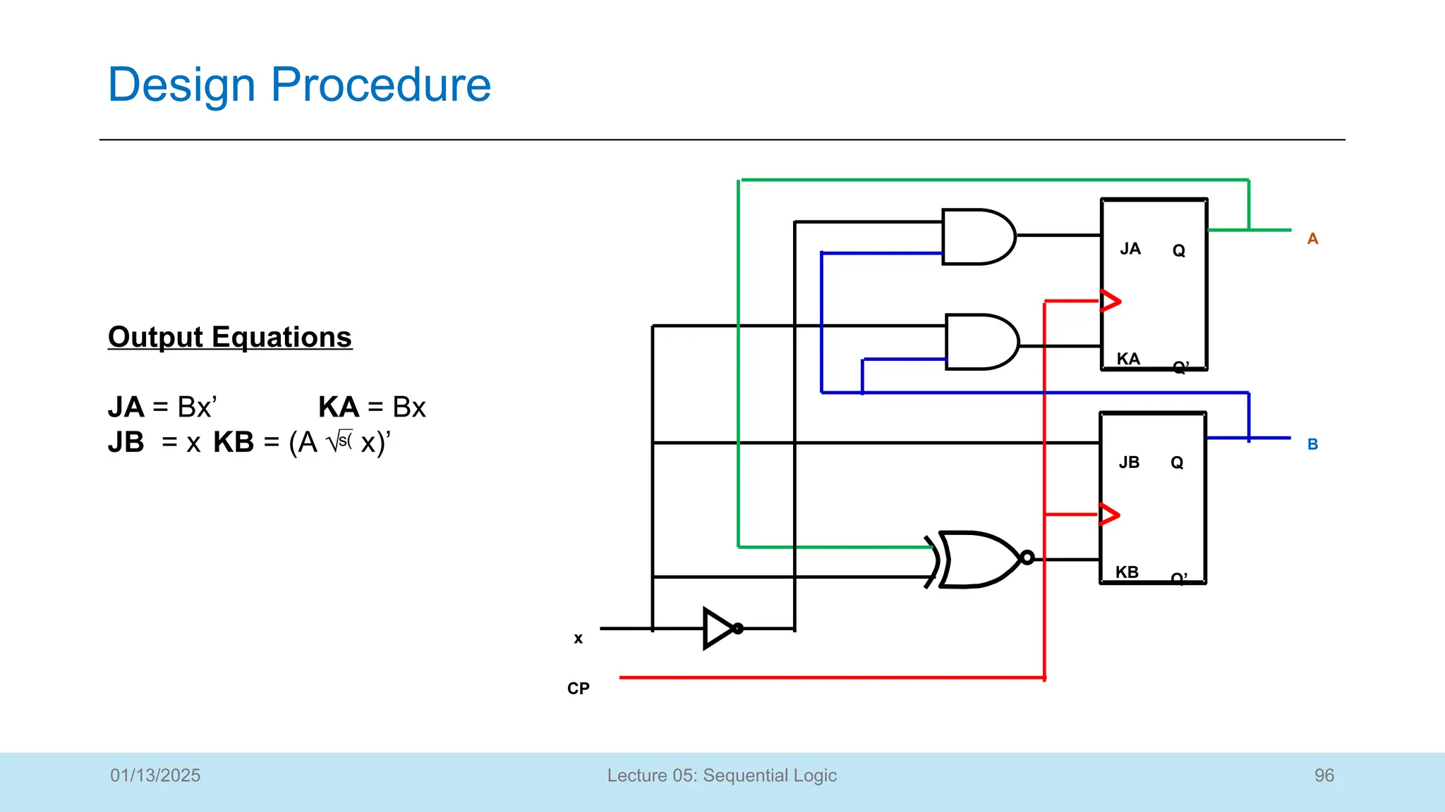
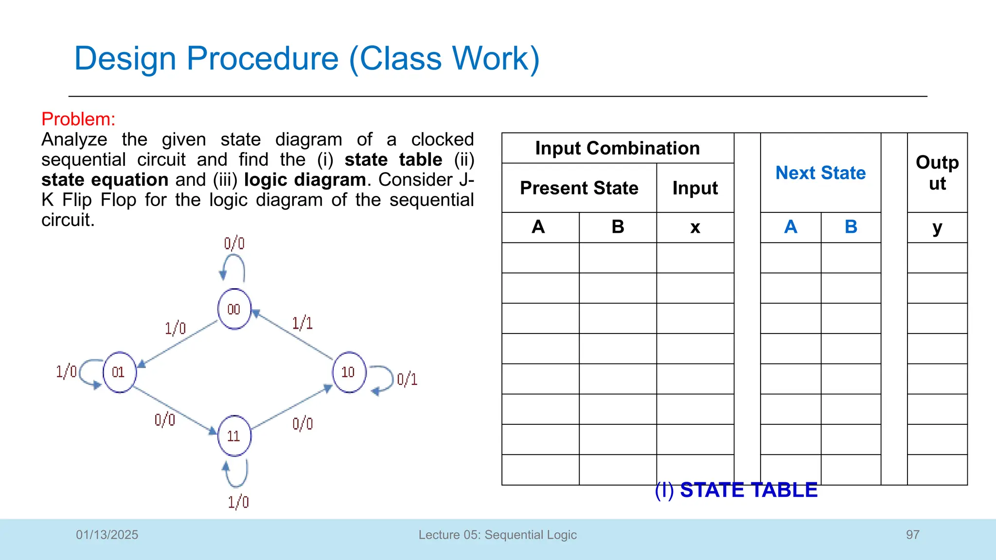
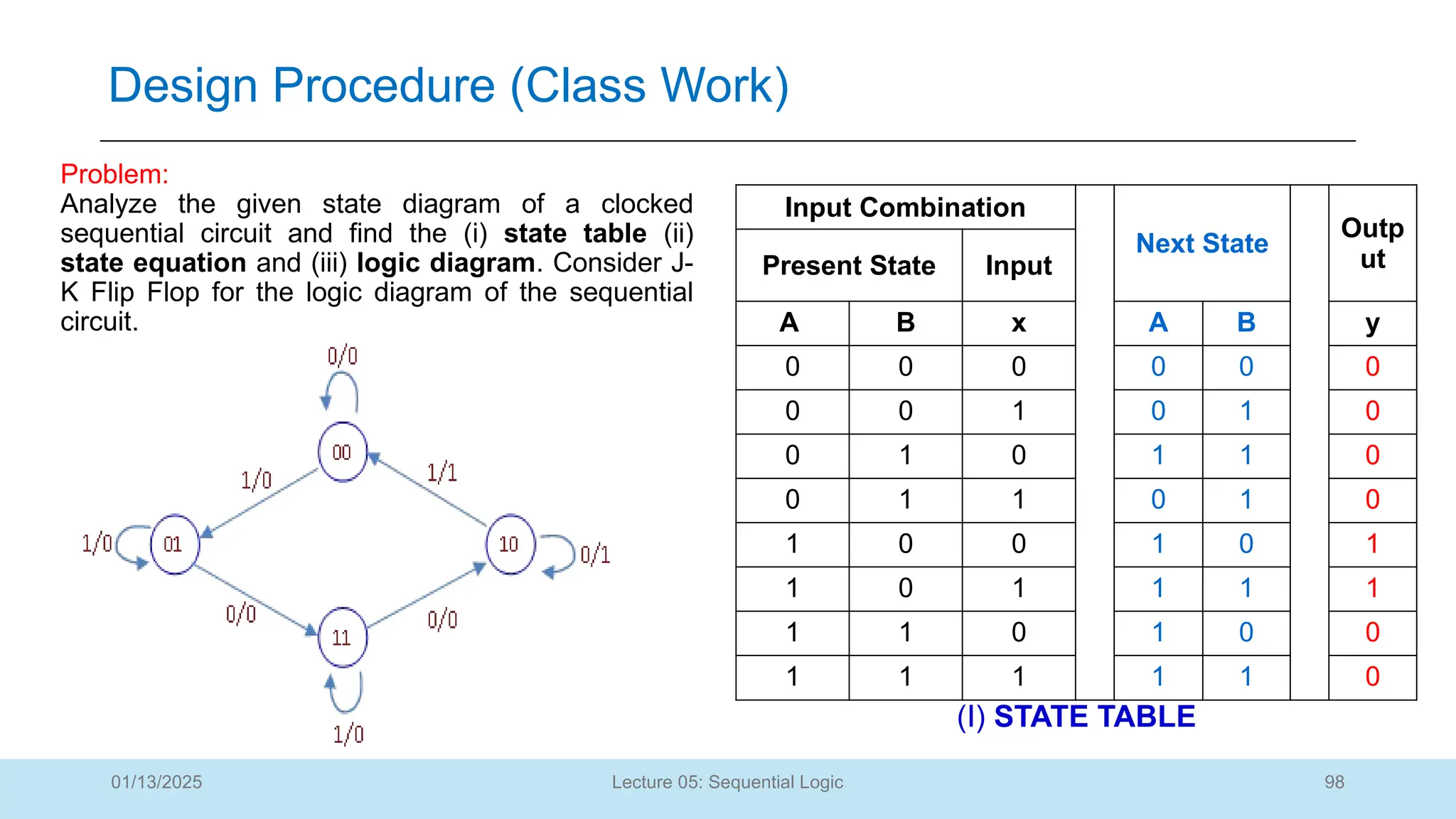
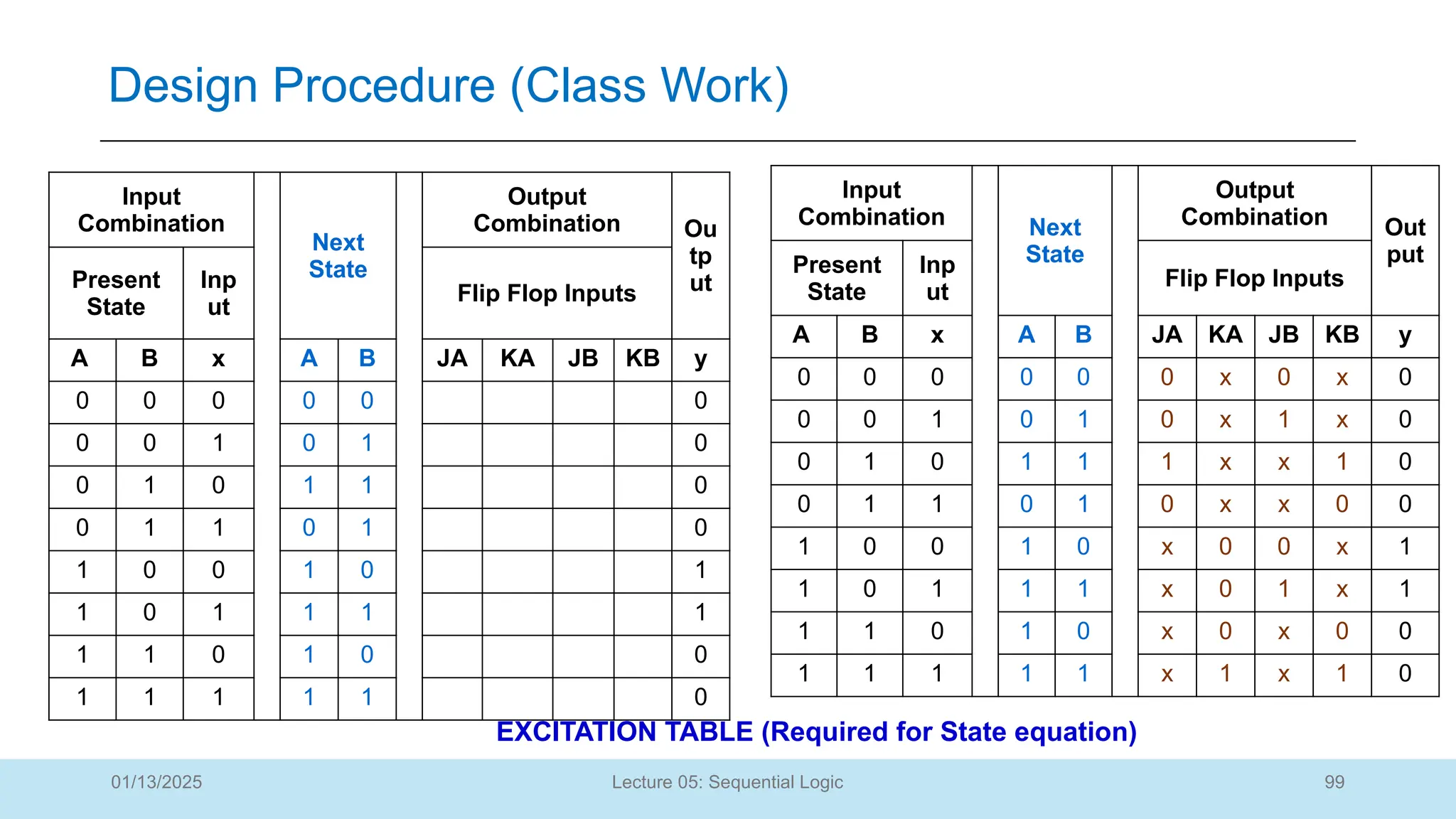
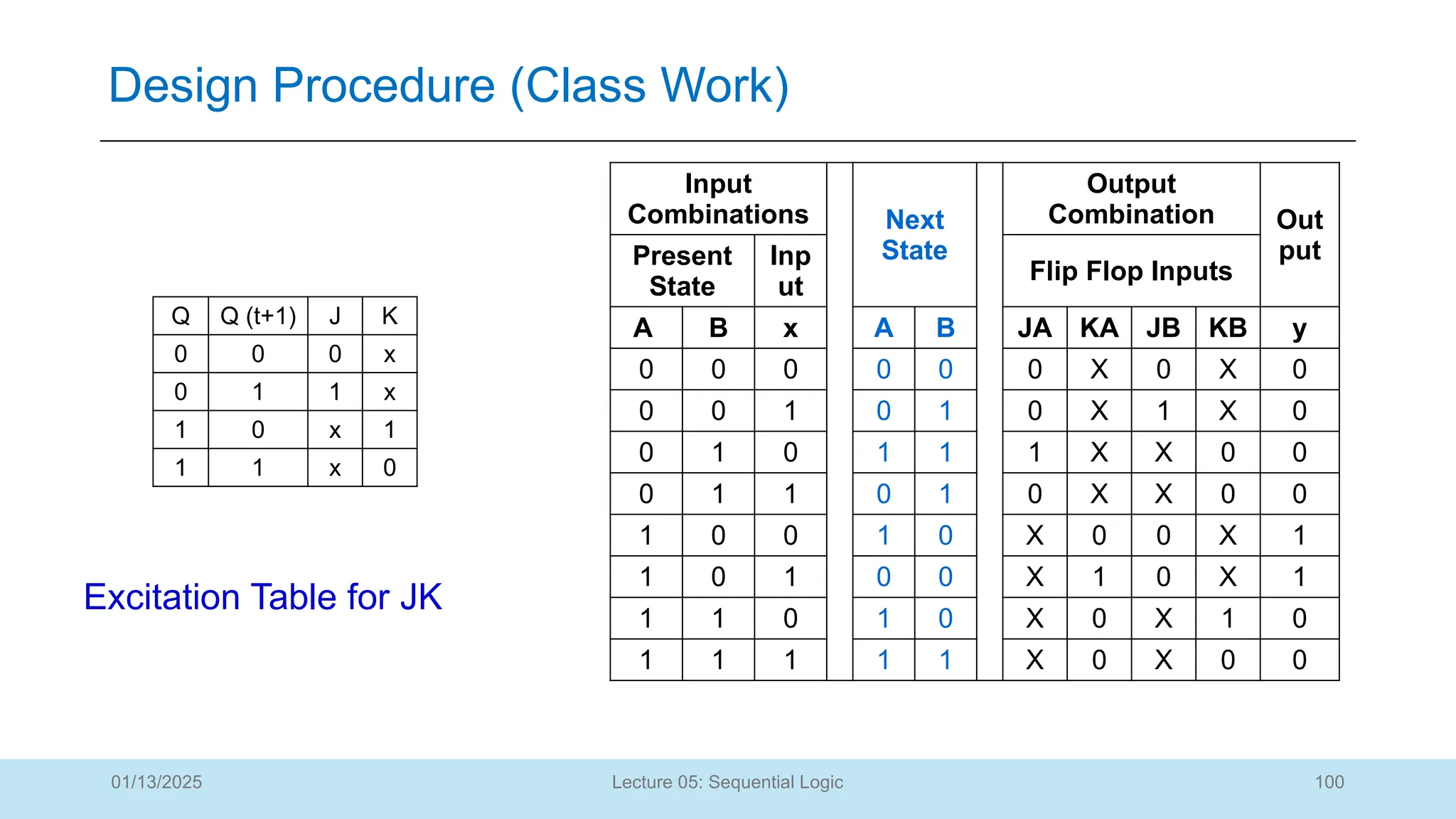
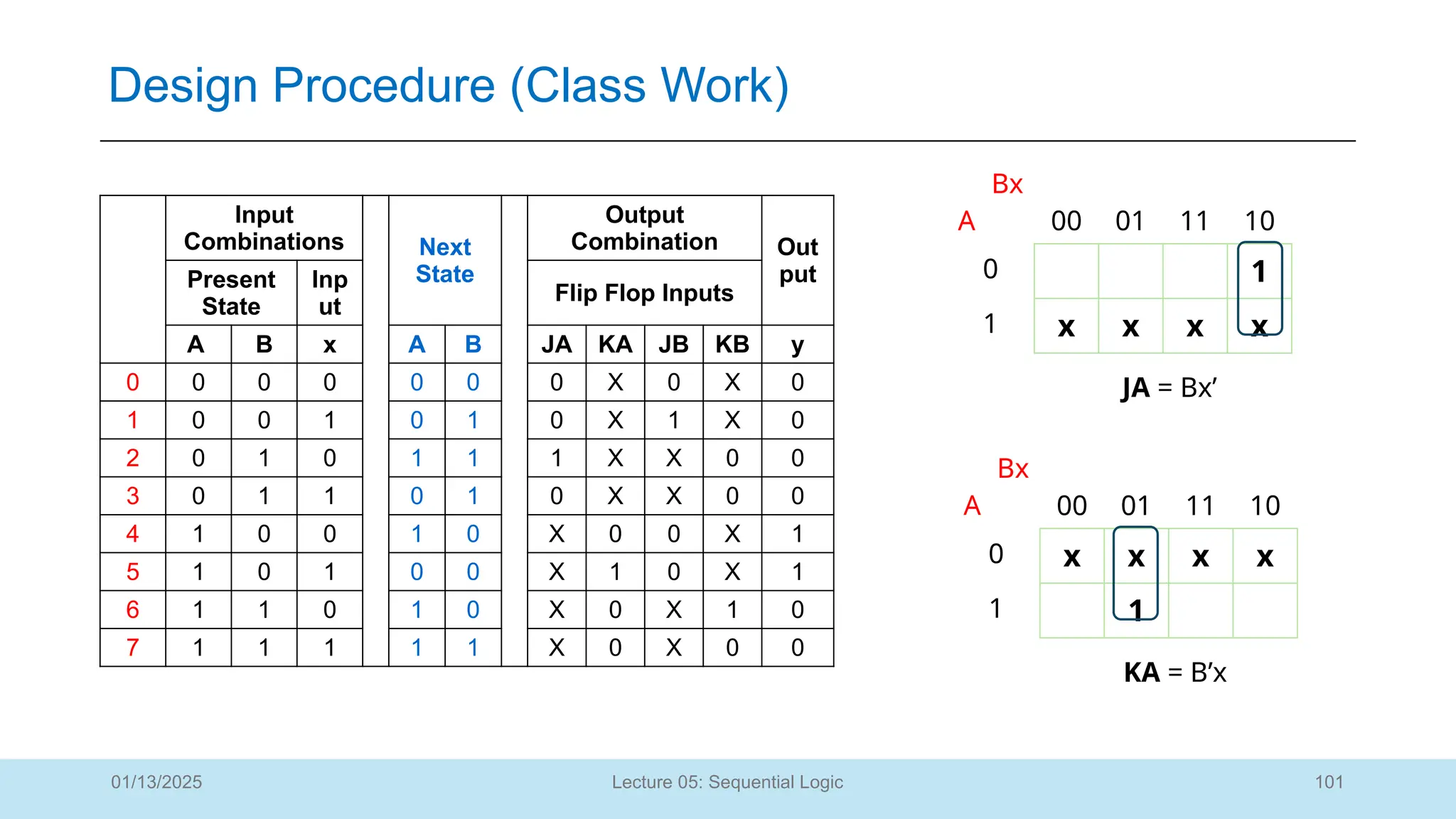
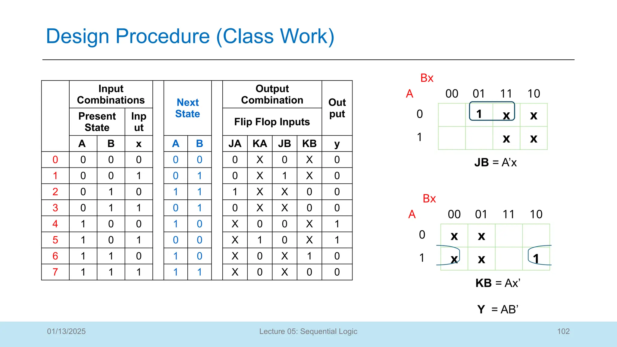
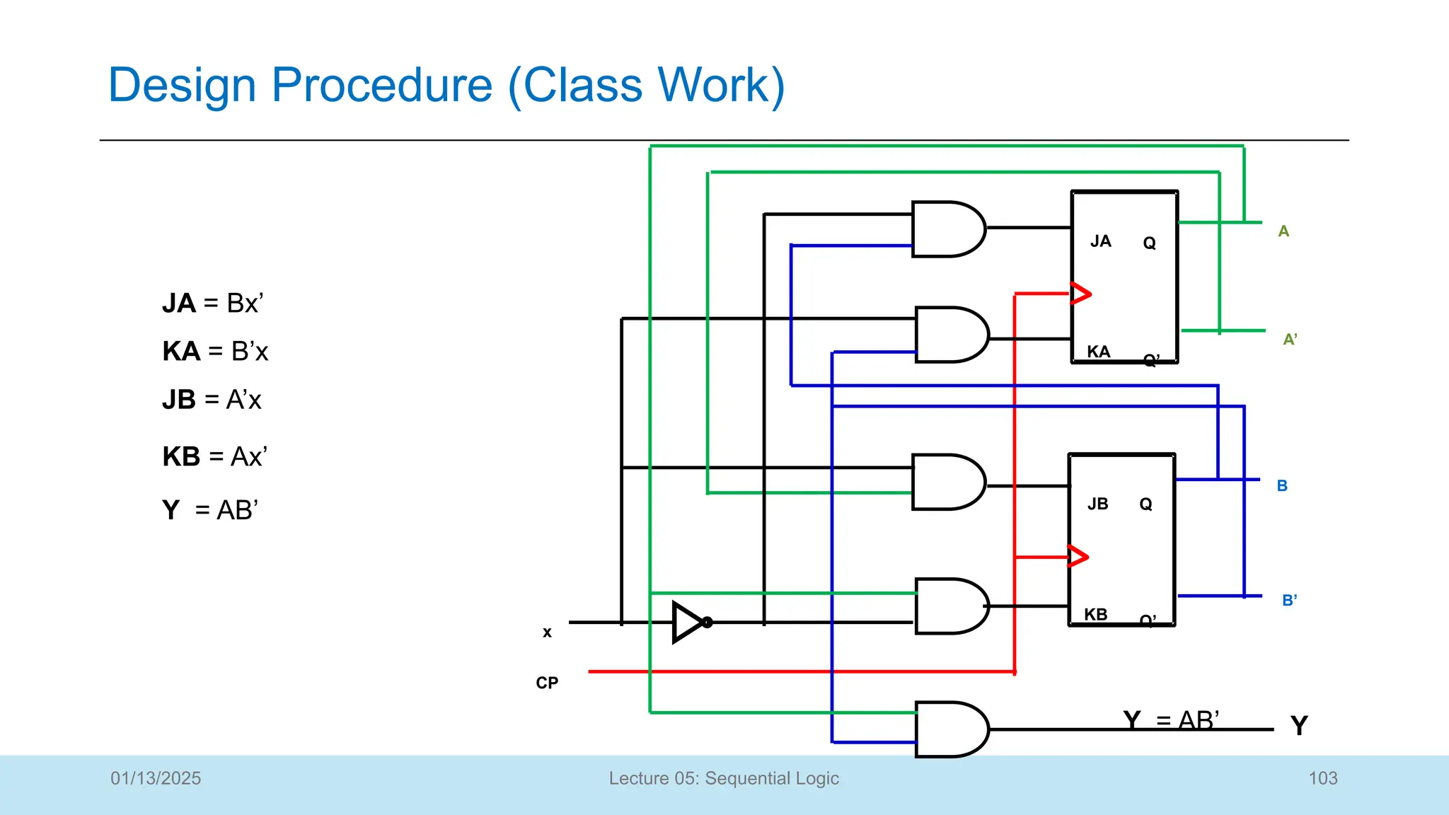
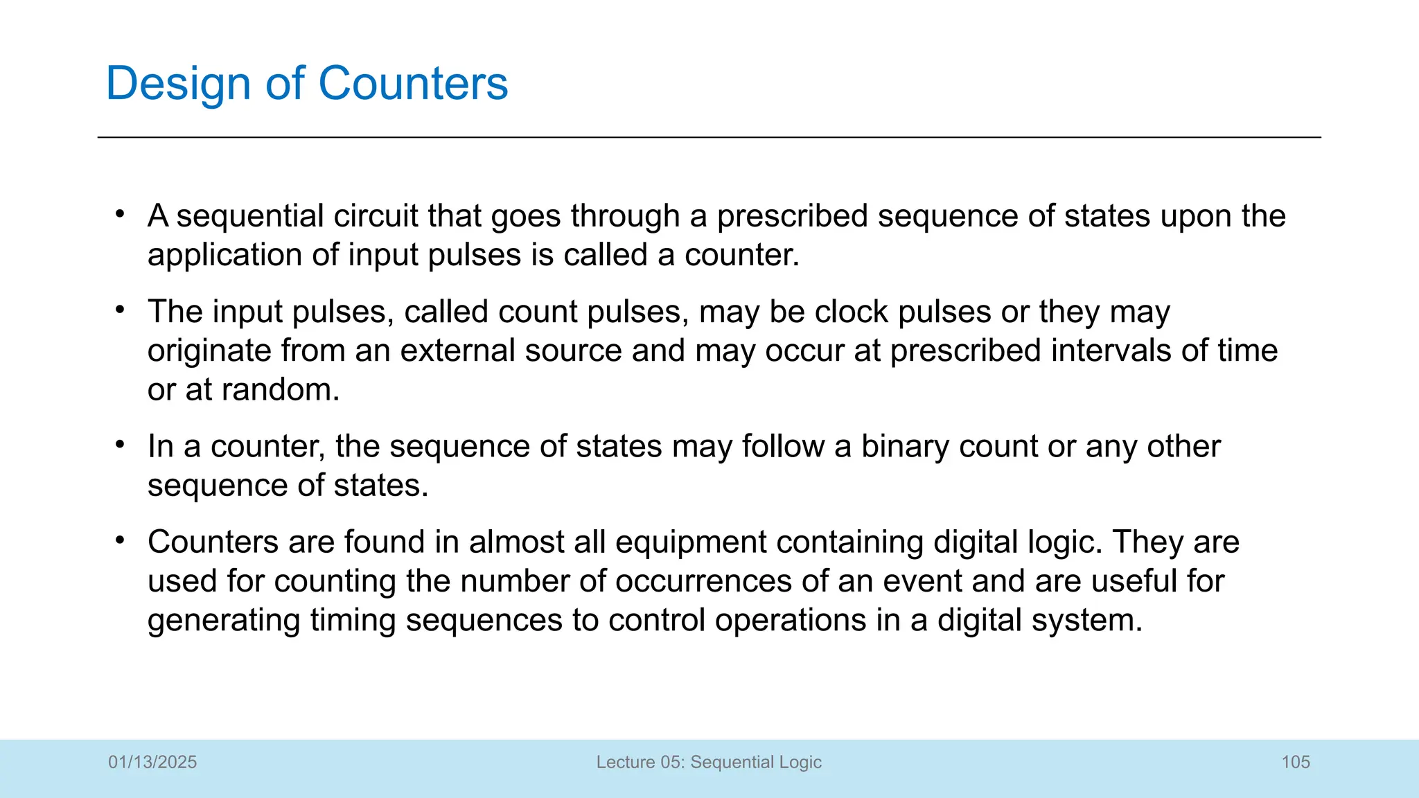
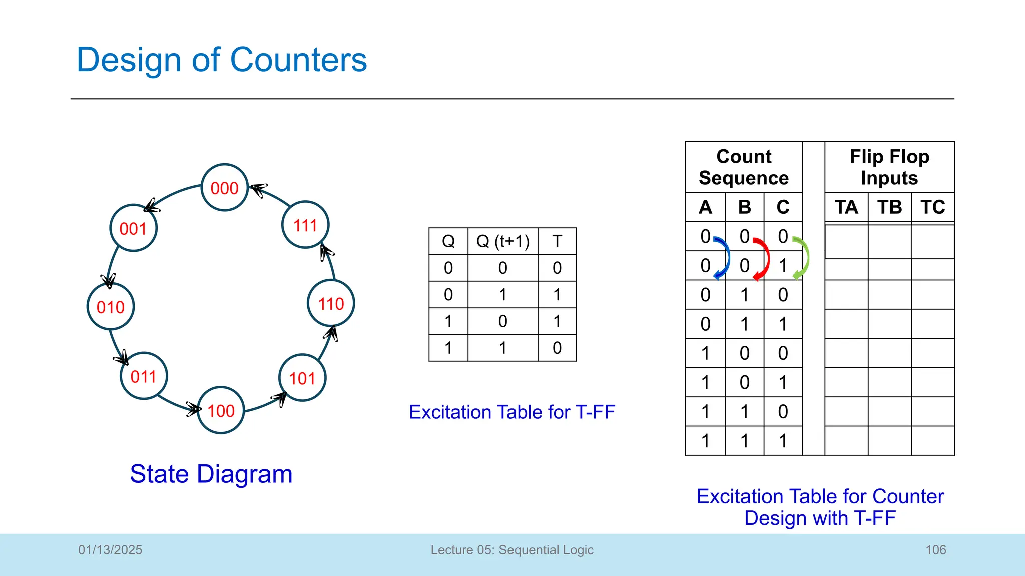
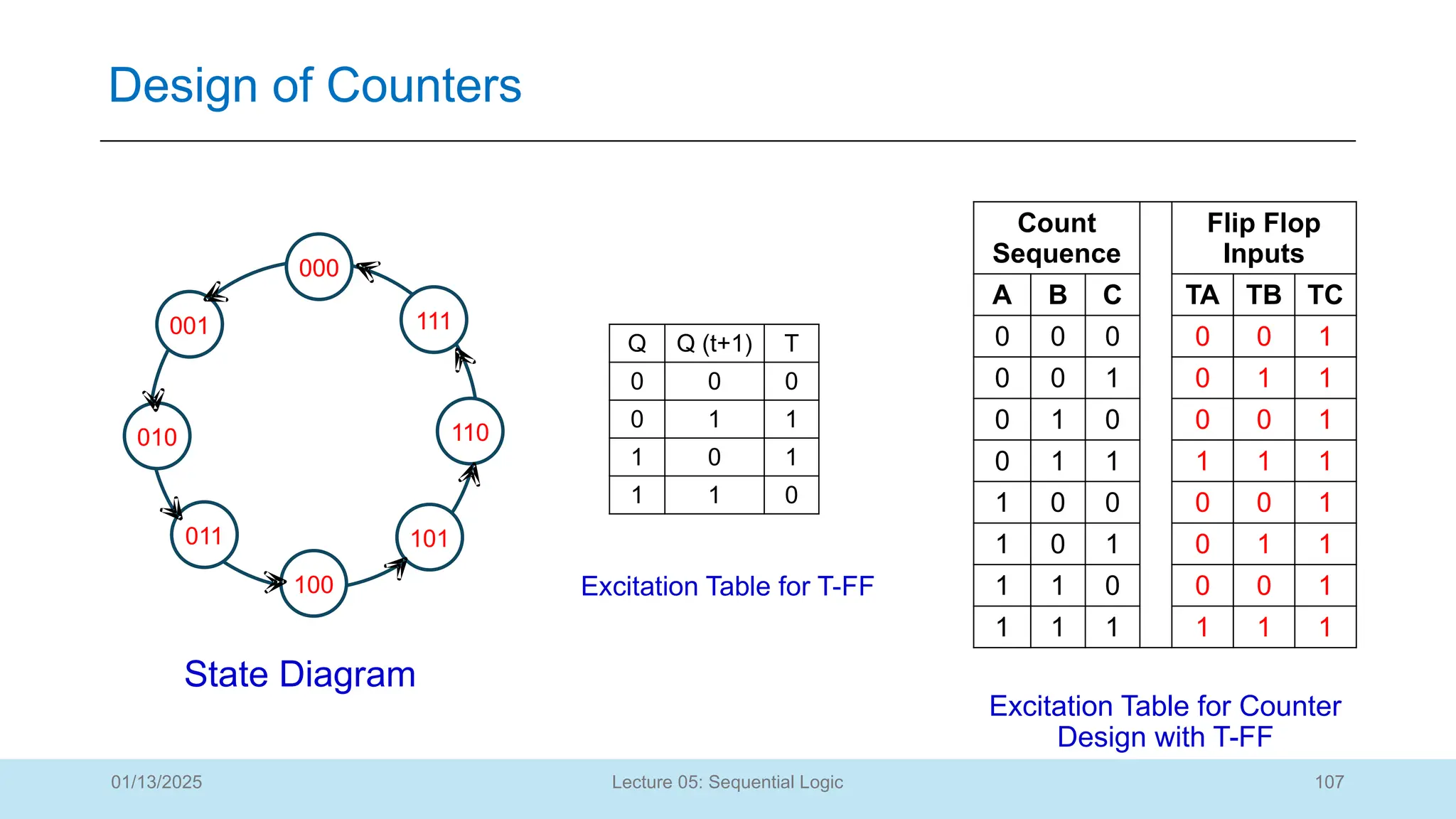
The document outlines a lecture on sequential logic circuits, focusing on components such as latches and flip-flops, and distinguishes between synchronous and asynchronous circuits. It covers various flip-flop types including S-R, D, JK, and T flip-flops, detailing their operations and truth tables. The lecture aims to equip students with the ability to analyze, design, and implement sequential circuits with practical applications in digital systems.
![14
Lecture 05: Sequential Logic
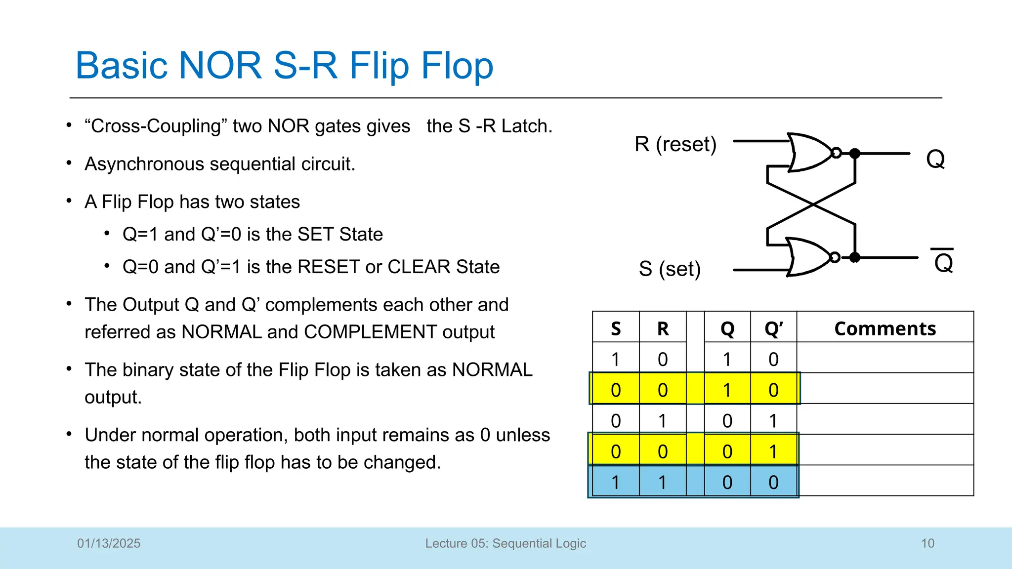
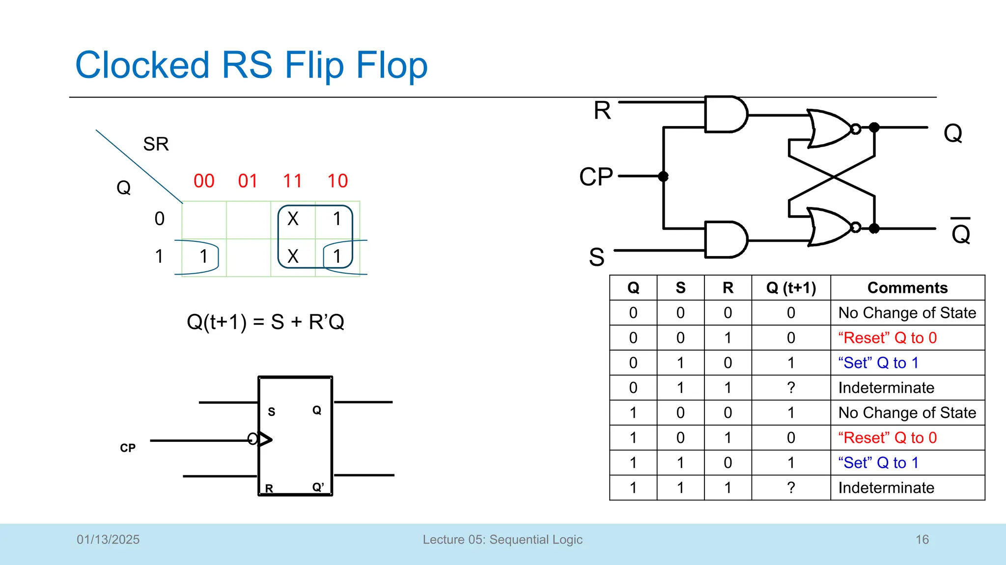
Clocked RS Flip Flop
01/13/2025
Q S R Q (t+1) Comments
0 0 0
0 0 1
0 1 0
0 1 1
1 0 0
1 0 1
1 1 0
1 1 1
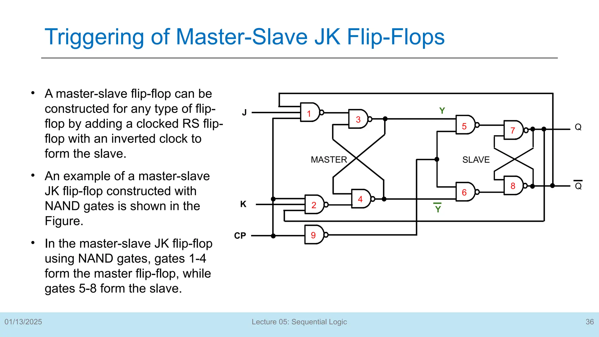
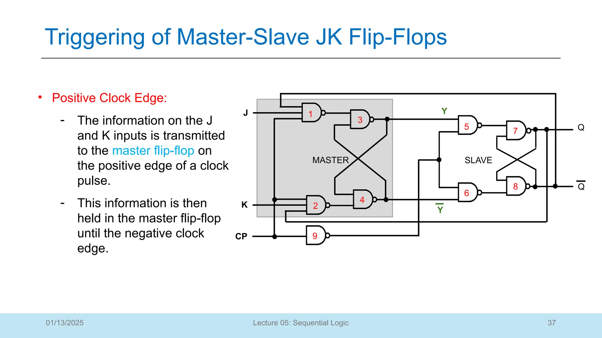
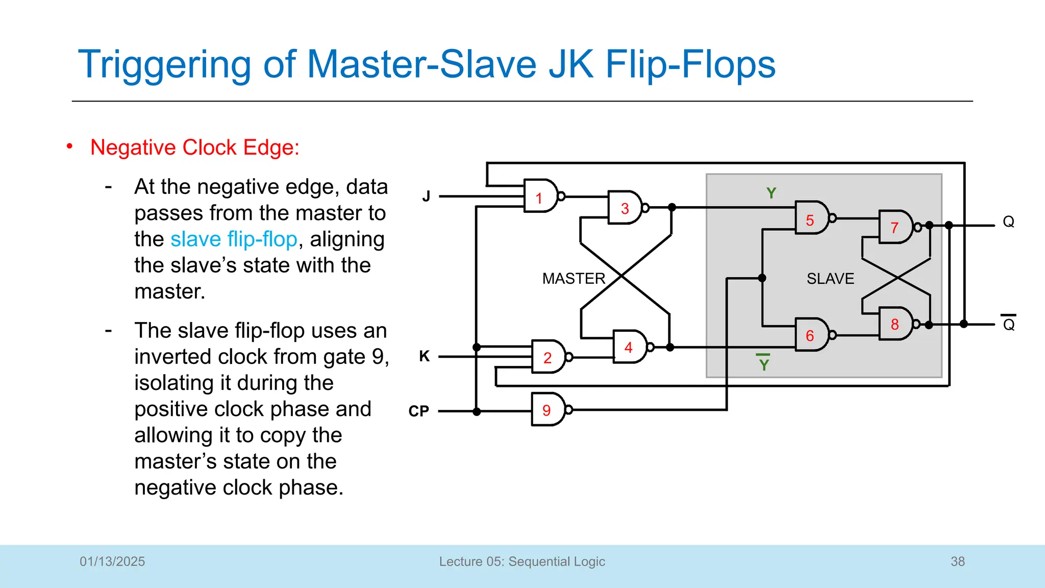
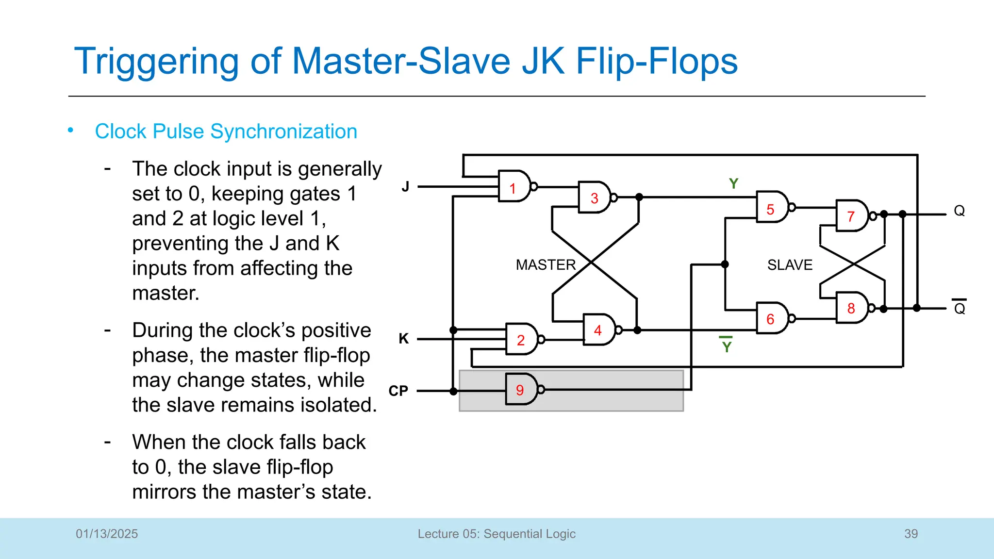
• Adding two AND gates to the basic S - R
NOR latch gives the clocked RS Latch:
• Has a time sequence behavior similar to the
basic S-R latch except that the S and R
inputs are only observed when the line C is
high.
• The table describes what happens after the
clock [at time (t+1)] based on:
• Present inputs (S,R) and
• Present State Q(t).
• CP means “Clock Pulse”.
• CP=1, S and R has input and the Flip Flop is in
operation
• CP=0, S=R=0;
R
S
Q
CP
Q](https://image.slidesharecdn.com/5-250113175116-a4591801/75/5-Digital-Logic-Design-Chap-06-Topic-11-12-13-14-15-16-17-Sequential-Circuit-1-pptx-14-2048.jpg)
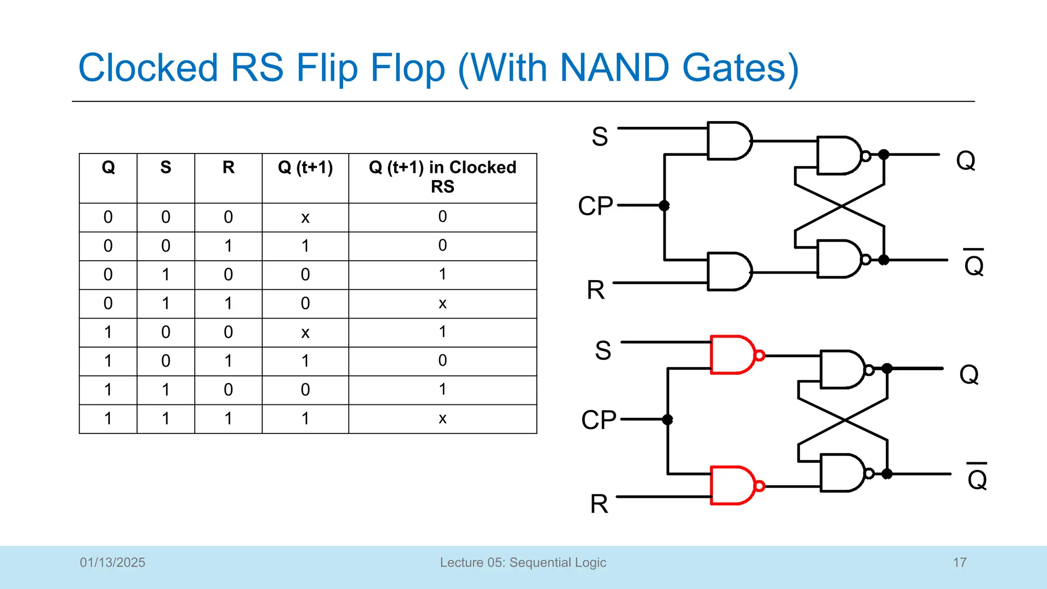
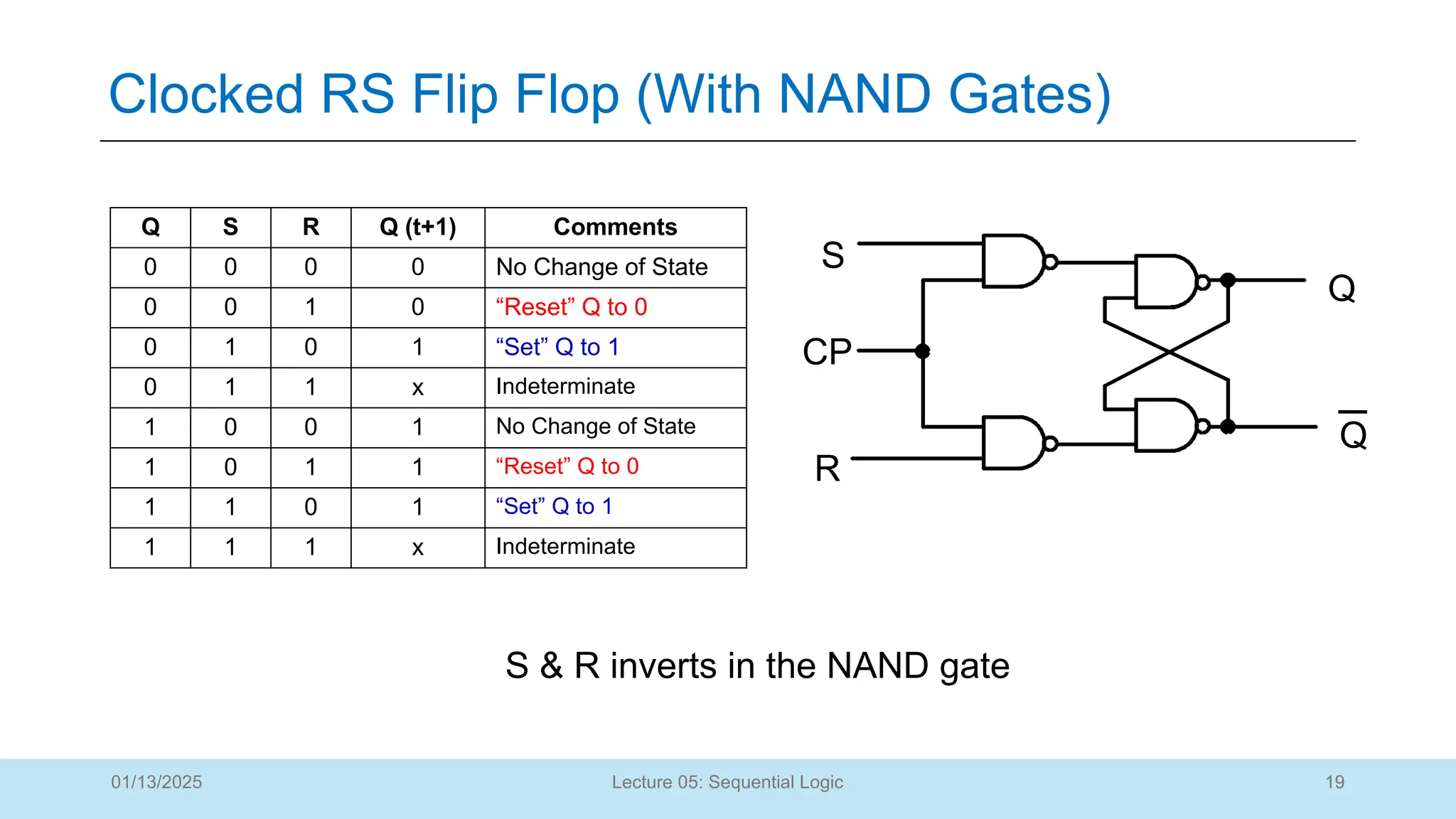
![15
Lecture 05: Sequential Logic
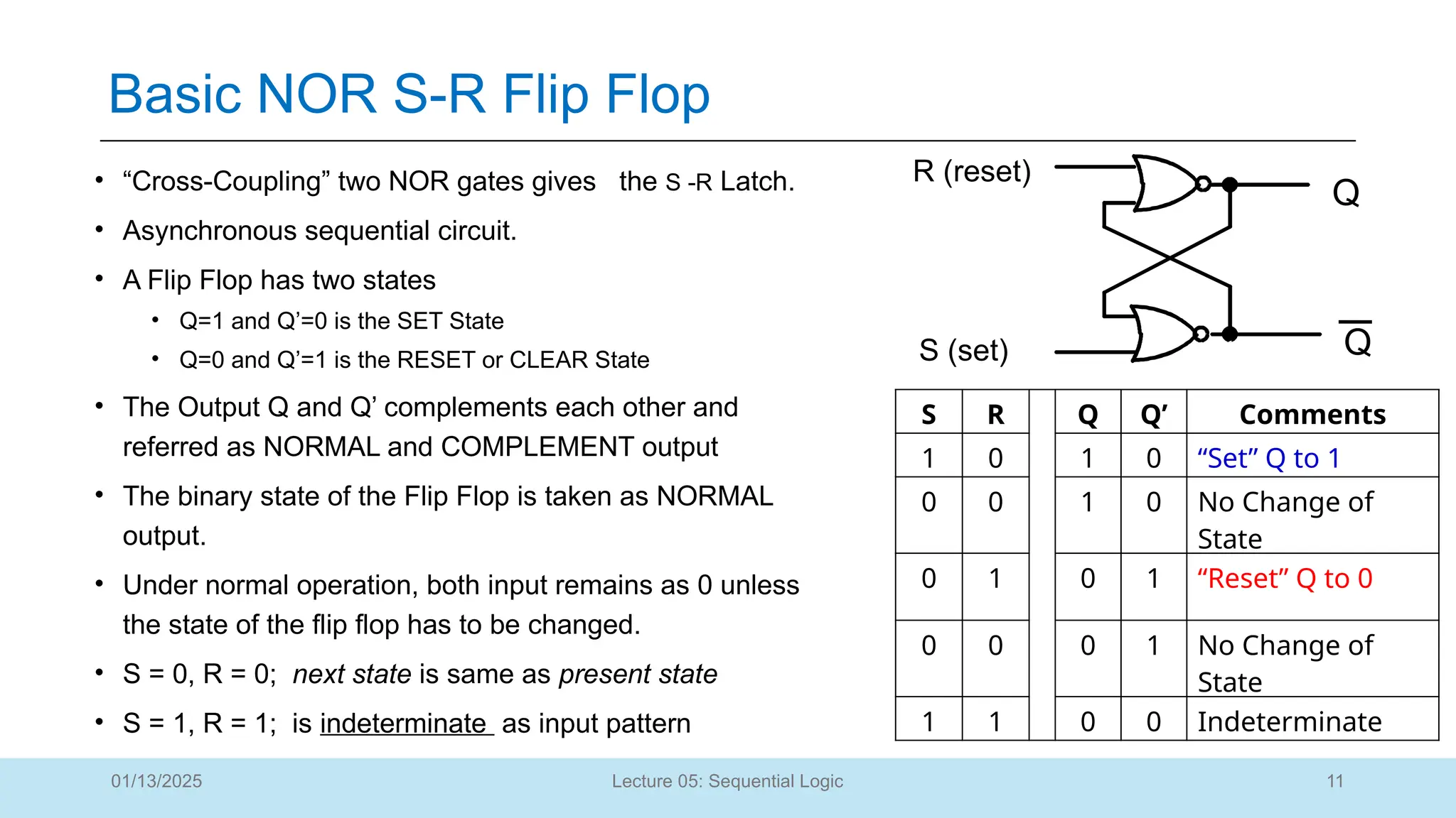
Clocked RS Flip Flop
01/13/2025
Q S R Q (t+1) Comments
0 0 0 0 No Change of State
0 0 1 0 “Reset” Q to 0
0 1 0 1 “Set” Q to 1
0 1 1 ? Indeterminate
1 0 0 1 No Change of State
1 0 1 0 “Reset” Q to 0
1 1 0 1 “Set” Q to 1
1 1 1 ? Indeterminate
• Adding two NAND gates to the basic S - R
NOR latch gives the clocked RS Latch:
• Has a time sequence behavior similar to the
basic S-R latch except that the S and R
inputs are only observed when the line C is
high.
• The table describes what happens after the
clock [at time (t+1)] based on:
• Present inputs (S,R) and
• Present State Q(t).
• CP means “Clock Pulse”.
• CP=1, S and R has input and the Flip Flop is in
operation
• CP=0, S=R=0;
R
S
Q
CP
Q](https://image.slidesharecdn.com/5-250113175116-a4591801/75/5-Digital-Logic-Design-Chap-06-Topic-11-12-13-14-15-16-17-Sequential-Circuit-1-pptx-15-2048.jpg)


![Unit 2[1] . technology with the informationpptx](https://cdn.slidesharecdn.com/ss_thumbnails/unit21-250302040241-815cd69e-thumbnail.jpg?width=640&height=640&fit=bounds)


