The document discusses the central processing unit (CPU) and provides details about its components and functions. It includes:
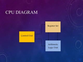
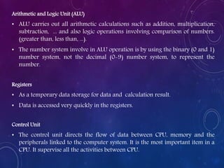
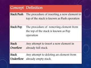
1) The CPU contains a register set, arithmetic logic unit (ALU), and control unit as its major parts. The register set stores data, instructions, addresses, and results. The ALU performs arithmetic and logic operations. The control unit directs data flow.
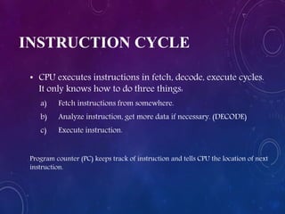
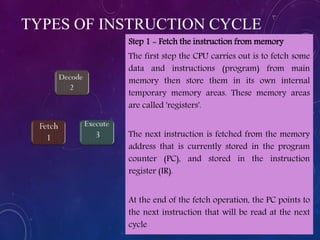
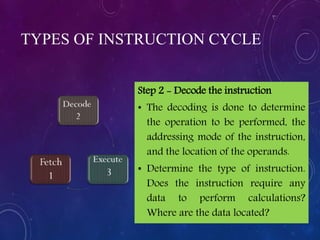
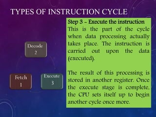
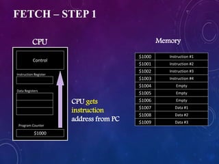
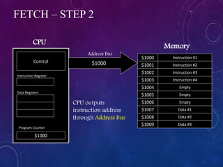
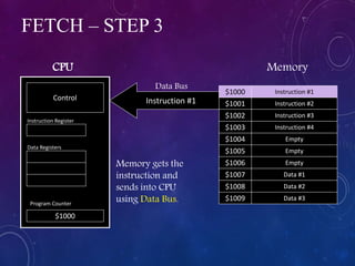
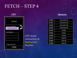
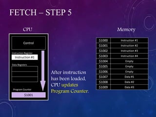
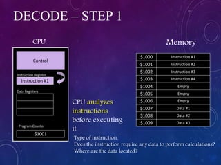
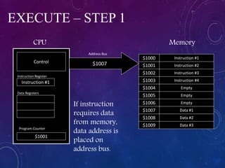
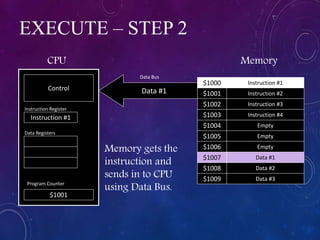
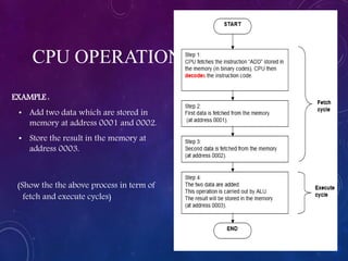
2) The CPU executes instructions through fetch, decode, and execute cycles. It fetches instructions from memory, decodes them to determine the operation, and executes the instruction by performing the operation.
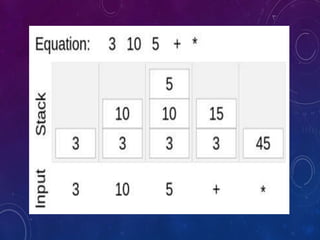
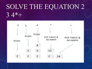
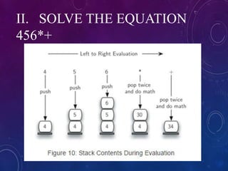
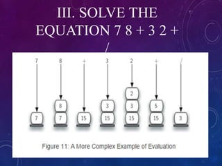
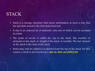
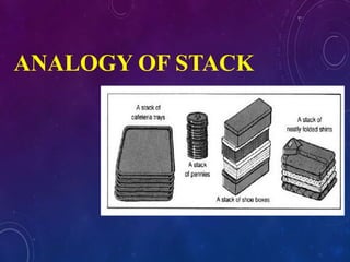
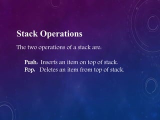
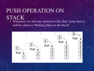
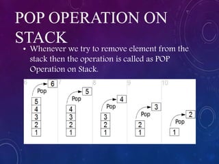
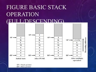
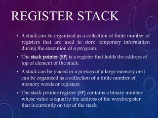
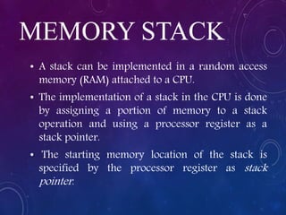
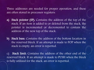
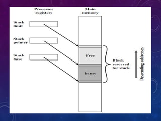
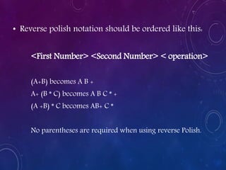
3) A stack is a data structure that follows last-in, first-out (LIFO) ordering. In computers


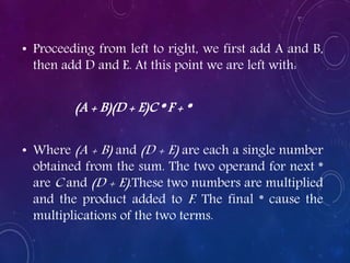
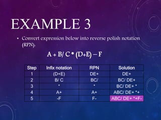
![• Consider the expression
(A + B) * [C * (D + E) + F]
• The expression can be converted to reverse Polish
notation, without the use of parentheses, by taking
the consideration of operation hierarchy.
• The converted expression is:
AB + DE + C * F + *](https://image.slidesharecdn.com/chapter4-190919120609/85/Central-Processing-Unit-45-320.jpg)
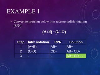
![EXAMPLE 4
• Convert expression below into reverse polish notation
(RPN):
(3 + 5) * [4 * (6 + 2) + 1]
Step Infix notation RPN Solution
1 (6 + 2) 6 2 + 6 2 +
2 4 * 4 * 6 2 + 4 *
3 + 1 1+ 6 2 + 4 *1+
4 (3 + 5) 3 5 + 3 5 + 6 2 + 4 *1+
5 * * 3 5 + 6 2 + 4 *1+*](https://image.slidesharecdn.com/chapter4-190919120609/85/Central-Processing-Unit-50-320.jpg)
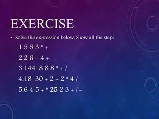
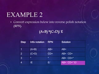
![EXERCISE
• Convert expression below to reverse polish
notation. Show all steps
1. (A + B) * [C * (D + E) + F]
2. A * B + C / D
3. A * (B + C) / D
4. A * (B + C / D)
5. ( (A * B) + (C / D) )
6. ((A * (B + C) ) / D)
7. (A * (B + (C / D) ) )](https://image.slidesharecdn.com/chapter4-190919120609/85/Central-Processing-Unit-51-320.jpg)