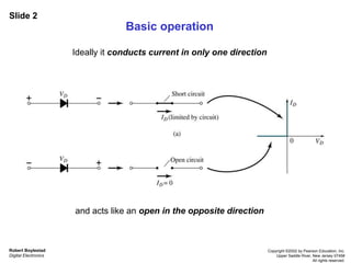
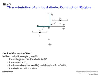
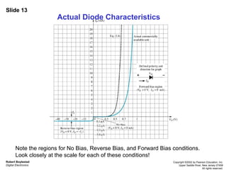
This document contains slides from a chapter about semiconductor diodes. It discusses the basic operation and characteristics of ideal diodes, including their conduction and non-conduction regions. Real diodes are not ideal due to the influence of majority and minority carriers. The document covers diode testing methods and specifications. It also introduces other types of diodes such as Zener diodes, light emitting diodes, and diode arrays.


![Slide 19
Robert Boylestad
Digital Electronics
Copyright ©2002 by Pearson Education, Inc.
Upper Saddle River, New Jersey 07458
All rights reserved.
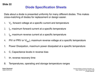
RD
= VD
/ID
[Formula 1.5]
For a specific applied DC voltage VD
,
the diode will have a specific current ID
,
and a specific resistance RD
.
The amount of resistance RD
, depends on the applied DC voltage.
DC or Static Resistance](https://image.slidesharecdn.com/ch01-semiconductordiodes-231222081720-1da84587/85/CH01-Semiconductor-Diodes-ppt-pdf-20-320.jpg)
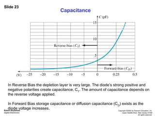
![Forward Bias region:
• The resistance depends on the amount of current (ID
) in the diode.
• The voltage across the diode is fairly constant (26mV for 25C).
• rB ranges from a typical 0.1 for high power devices to 2 for low power, general
purpose diodes. In some cases rB can be ignored.
Reverse Bias region:
The resistance is essentially infinite. The diode acts like an open.
Slide 20
Robert Boylestad
Digital Electronics
Copyright ©2002 by Pearson Education, Inc.
Upper Saddle River, New Jersey 07458
All rights reserved.
AC or Dynamic Resistance
[Formula 1.8]](https://image.slidesharecdn.com/ch01-semiconductordiodes-231222081720-1da84587/85/CH01-Semiconductor-Diodes-ppt-pdf-21-320.jpg)
![Slide 21
Robert Boylestad
Digital Electronics
Copyright ©2002 by Pearson Education, Inc.
Upper Saddle River, New Jersey 07458
All rights reserved.
AC resistance can be determined by picking 2 points on the characteristic curve
developed for a particular circuit.
[Formula 1.9]
Average AC Resistance](https://image.slidesharecdn.com/ch01-semiconductordiodes-231222081720-1da84587/85/CH01-Semiconductor-Diodes-ppt-pdf-22-320.jpg)