This document is a lecture note on semiconductor diodes and their applications. It discusses ideal diodes, practical diode models, diode resistance, and applications of diodes such as in rectifiers. The key points are:
- An ideal diode allows current in one direction and blocks it in the other. Real diodes have resistance and a voltage drop.
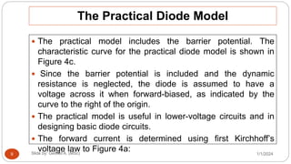
- Diode models range from ideal to practical (with voltage drop) to complete (with forward and reverse resistance).
- Diode resistance depends on operating point and is lower at higher currents. Dynamic resistance also depends on operating point.
- Applications include rectifiers, voltage multiplication, logic gates, and more. Rectifiers are used to convert AC to