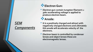
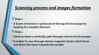
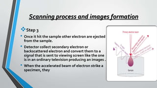
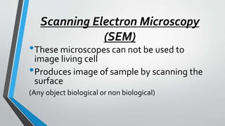
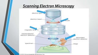
Scanning Electron Microscopy
Presented To:
Sir Zahid Qamar
Presented by:
Numair Zeeshan
Naeem Akhtar Khan
Outline
• Basic info
• Why we use SEM
• Principal
• Instrumentation
• Detection in Sem
• Working
• Application
• Advantages and Disadvantage
WhyWe Use SEM
• When we want to study a sample in a depth
• By using SEM create magnified image
• Sem has high resolution power
• Depth resolution 10 -100nm
• Lateral resolution 1-10nm
Electron Microscope
• Electron Microscope is a type of microscope that use a beam
of electron to create an image of specimen.
• Have a higher resolving power then light microscope and can
reveal the structure of smaller object.
• Electron are very sensitive to magnetic field and can
therefore control by changing the current through lenses.
• Use to investigate structure of wide range of biological and
inorganic specimen including cell microorganism etc.
Principle
•When accelerated
primary electron strikes
the sample it produces
secondary electron these
secondary electron are
collected by positive
charge electron detector
which in turn gives three-
dimensional image of the
sample.
SEM
Components
Electron Gun:
• Electron gun contain tungsten filament 1-
30kv accelerating voltage is applied to
produce electron beam.
Anode:
• It is a positively charged and attract with
negatively charged electrons and ultimately
this anode will accelerate velocity of the
electrons.
• Electron beam is controlled by condenser
lenses and object lenses these are
electromagnetic lenses.
• Electron beam is controlled by condenser lenses and object lenses
these are electromagnetic lenses
Condenser lenses:
• These lenses will focus electron beam toward, the objective
lenses.
Objective lenses:
• The lens will again focus the electron beam toward, the sample.
Detection in SEM
There is three types of detection is possible in SEM
Secondary electron detector
•SE ARE most abundant in the case of SEM and detected by
suitable detector ET detector are most commonly used for
detection secondary electron.
•ET detector contain Biased grid which is positively charged
to attract the secondary electron.This will create basic
image of sem.
BACKSCATTERD ELECTRON
•Energy of backscattered electron are higher then,
secondary electron so ET detector of verifying
voltage can differentiate betweenTHEM.
X-rays Detector
•Inside the sample holder x ray detector is placed
and it will detect x-ray imaged by sample.
•THIS detection process is known as EDX
Scanning process and images formation
Step 1
• A beam of electron is produced at the top of microscope by
heating of a metallic filament.
Step 2
• Electron beam a vertically path through column of microscope.
• It makes its way through electro magnetic lenses which focus
and direct the beam towards the sample.
Scanning process and images formation
Step 3
• Once it hit the sample other electron are ejected
from the sample.
• Detector collect secondary electron or
backscattered electron and convert them to a
signal that is sent to viewing screen like the one
is in an ordinary television producing an images .
• When the accelerated beam of electron strike a
specimen, they
Sample
preparation
Wash
Dry
Dehydration
(Acetone + Alcohol)
Coating
Scanning Electron Microscopy
(SEM)
•These microscopes can not be used to
image living cell
•Produces image of sample by scanning the
surface
(Any object biological or non biological)
Scanning Electron Microscopy
SEM Application
• SEMs have a variety of applications in a number of
scientific and industry-related fields, especially where
characterizations of solid materials is beneficial.
• For investigation of viruses, structure.
• 3D tissue imaging.
• Insect and other Micro-organism and Component
visualize.
• A SEM can detect and analyze surface fractures, provide
information in microstructures, examine surface
contaminations, provide qualitative chemical analyses and
identify crystalline structures.
• SEMs can be as essential research tool in fields such as life
science, biology, gemology, medical and forensic science,
metallurgy.
• In addition, SEMs have practical industrial and
technological applications such as semiconductor
inspection, production line of miniscule products and
assembly of microchips for computers.
Advantages of SEM
SEM are also easy to
operate with the proper
training and advances in
computer technology and
associated software make
operation user friendly
This instrument work fast,
often completing SEI, BSI
and EDS analysis in less
then 5 Minutes.
Magnifies object more
then 500000X
Most SEM sample require
minimal preparation
action.
Disadvantages of SEM
VERY LARGE
(OPERATED IN
SPECIAL ROOM).
PREPARATIONOF
MATERIAL IS
LENGTHY.
REQUIRE EXPERTISE EXPENSIVETO
PURCHASEAND
OPERATE.
Scanning Electron Microscopy

Scanning Electron Microscopy

  • 2.
    Scanning Electron Microscopy PresentedTo: Sir Zahid Qamar Presented by: Numair Zeeshan Naeem Akhtar Khan
  • 3.
    Outline • Basic info •Why we use SEM • Principal • Instrumentation • Detection in Sem • Working • Application • Advantages and Disadvantage
  • 4.
    WhyWe Use SEM •When we want to study a sample in a depth • By using SEM create magnified image • Sem has high resolution power • Depth resolution 10 -100nm • Lateral resolution 1-10nm
  • 5.
    Electron Microscope • ElectronMicroscope is a type of microscope that use a beam of electron to create an image of specimen. • Have a higher resolving power then light microscope and can reveal the structure of smaller object. • Electron are very sensitive to magnetic field and can therefore control by changing the current through lenses. • Use to investigate structure of wide range of biological and inorganic specimen including cell microorganism etc.
  • 6.
    Principle •When accelerated primary electronstrikes the sample it produces secondary electron these secondary electron are collected by positive charge electron detector which in turn gives three- dimensional image of the sample.
  • 7.
    SEM Components Electron Gun: • Electrongun contain tungsten filament 1- 30kv accelerating voltage is applied to produce electron beam. Anode: • It is a positively charged and attract with negatively charged electrons and ultimately this anode will accelerate velocity of the electrons. • Electron beam is controlled by condenser lenses and object lenses these are electromagnetic lenses.
  • 8.
    • Electron beamis controlled by condenser lenses and object lenses these are electromagnetic lenses Condenser lenses: • These lenses will focus electron beam toward, the objective lenses. Objective lenses: • The lens will again focus the electron beam toward, the sample.
  • 9.
    Detection in SEM Thereis three types of detection is possible in SEM Secondary electron detector •SE ARE most abundant in the case of SEM and detected by suitable detector ET detector are most commonly used for detection secondary electron. •ET detector contain Biased grid which is positively charged to attract the secondary electron.This will create basic image of sem.
  • 10.
    BACKSCATTERD ELECTRON •Energy ofbackscattered electron are higher then, secondary electron so ET detector of verifying voltage can differentiate betweenTHEM. X-rays Detector •Inside the sample holder x ray detector is placed and it will detect x-ray imaged by sample. •THIS detection process is known as EDX
  • 11.
    Scanning process andimages formation Step 1 • A beam of electron is produced at the top of microscope by heating of a metallic filament. Step 2 • Electron beam a vertically path through column of microscope. • It makes its way through electro magnetic lenses which focus and direct the beam towards the sample.
  • 12.
    Scanning process andimages formation Step 3 • Once it hit the sample other electron are ejected from the sample. • Detector collect secondary electron or backscattered electron and convert them to a signal that is sent to viewing screen like the one is in an ordinary television producing an images . • When the accelerated beam of electron strike a specimen, they
  • 13.
  • 14.
    Scanning Electron Microscopy (SEM) •Thesemicroscopes can not be used to image living cell •Produces image of sample by scanning the surface (Any object biological or non biological)
  • 15.
  • 17.
    SEM Application • SEMshave a variety of applications in a number of scientific and industry-related fields, especially where characterizations of solid materials is beneficial. • For investigation of viruses, structure. • 3D tissue imaging. • Insect and other Micro-organism and Component visualize.
  • 18.
    • A SEMcan detect and analyze surface fractures, provide information in microstructures, examine surface contaminations, provide qualitative chemical analyses and identify crystalline structures. • SEMs can be as essential research tool in fields such as life science, biology, gemology, medical and forensic science, metallurgy. • In addition, SEMs have practical industrial and technological applications such as semiconductor inspection, production line of miniscule products and assembly of microchips for computers.
  • 20.
    Advantages of SEM SEMare also easy to operate with the proper training and advances in computer technology and associated software make operation user friendly This instrument work fast, often completing SEI, BSI and EDS analysis in less then 5 Minutes. Magnifies object more then 500000X Most SEM sample require minimal preparation action.
  • 21.
    Disadvantages of SEM VERYLARGE (OPERATED IN SPECIAL ROOM). PREPARATIONOF MATERIAL IS LENGTHY. REQUIRE EXPERTISE EXPENSIVETO PURCHASEAND OPERATE.