Downloaded 18 times

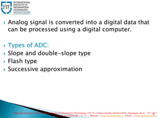
![ Characteristics of ADC[2]:
1. Resolution:
ADC has n- bit resolution(where n=8,10,12,16,24
bits)
Higher the resolution smaller the step size
If ADC has 8 bit resolution means 2^8= 256(No. of
steps)
Applied voltage is Vref=5v then 5/256=19.53 mv
(step size)
2. Conversion time:
The time it takes for the converting analog input to
digital output Vref:It is input voltage used for the
reference voltage
Vref/no. of steps(Vref is responsible for step size)
Hope Foundation’s International Institute of Information Technology, I²IT, P-14 Rajiv Gandhi Infotech Park, Hinjawadi, Pune - 411 057
Tel - +91 20 22933441 / 2 / 3 | Website - www.isquareit.edu.in ; Email - info@isquareit.edu.in
4](https://image.slidesharecdn.com/picmicrocontrolleradcashvinik-190228132818/85/PIC-Microcontroller-ADC-Interfacing-4-320.jpg)
![ Characteristics of ADC:
3. Digital data output:
8 bit ADC, we have 8bit digital data output of D0
–D7
Dout=Vin/step size[2]
Hope Foundation’s International Institute of Information Technology, I²IT, P-14 Rajiv Gandhi Infotech Park, Hinjawadi, Pune - 411 057
Tel - +91 20 22933441 / 2 / 3 | Website - www.isquareit.edu.in ; Email - info@isquareit.edu.in
5](https://image.slidesharecdn.com/picmicrocontrolleradcashvinik-190228132818/85/PIC-Microcontroller-ADC-Interfacing-5-320.jpg)

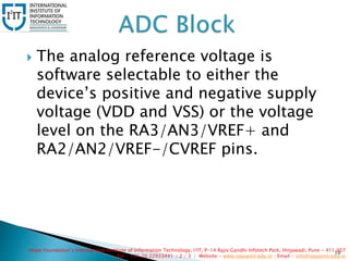
![Configuring Registers
Hope Foundation’s International Institute of Information Technology, I²IT, P-14 Rajiv Gandhi Infotech Park, Hinjawadi, Pune - 411 057
Tel - +91 20 22933441 / 2 / 3 | Website - www.isquareit.edu.in ; Email - info@isquareit.edu.in7
The PIC18 Microcontroller
- The A/D converter has the following
registers[1]:
• A/D Control Register 0 (ADCON0)
• A/D Control Register 1 (ADCON1)
• A/D Control Register 2 (ADCON2)
• A/D Result High Register (ADRESH)
• A/D Result Low Register (ADRESL)](https://image.slidesharecdn.com/picmicrocontrolleradcashvinik-190228132818/85/PIC-Microcontroller-ADC-Interfacing-7-320.jpg)
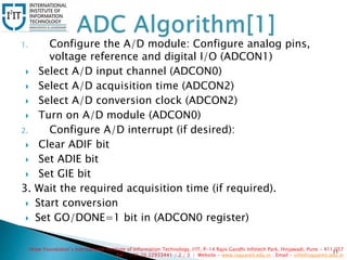
![Hope Foundation’s International Institute of Information Technology, I²IT, P-14 Rajiv Gandhi Infotech Park, Hinjawadi, Pune - 411 057
Tel - +91 20 22933441 / 2 / 3 | Website - www.isquareit.edu.in ; Email - info@isquareit.edu.in
8
Figure No. 1: Block diagram of ADC in PIC18f4550[1]](https://image.slidesharecdn.com/picmicrocontrolleradcashvinik-190228132818/85/PIC-Microcontroller-ADC-Interfacing-8-320.jpg)
![[1] Microchip datasheet of PIC18F2455/2550/4455/4550
[2] Muhamad Ali Mazidi,Rolind D Mckinly,”PIC
microcontroller and embedded systems”Pearson
publication.
Hope Foundation’s International Institute of Information Technology, I²IT, P-14 Rajiv Gandhi Infotech Park, Hinjawadi, Pune - 411 057
Tel - +91 20 22933441 / 2 / 3 | Website - www.isquareit.edu.in ; Email - info@isquareit.edu.in
13](https://image.slidesharecdn.com/picmicrocontrolleradcashvinik-190228132818/85/PIC-Microcontroller-ADC-Interfacing-13-320.jpg)

The document outlines the features and characteristics of the ADC in the PIC18 microcontroller, particularly highlighting its 10-bit resolution and multiple input channels. It provides details on ADC types, key characteristics such as resolution, conversion time, and digital output, as well as the necessary control registers for configuration. Additionally, it describes the configuration and operational steps required for utilizing the ADC effectively.


![Interfacing technique with 8085- ADC[0808]](https://cdn.slidesharecdn.com/ss_thumbnails/adc-160307140900-thumbnail.jpg?width=640&height=640&fit=bounds)