DAC and ADCInterfacing in
Microcontroller
Prof.M.Syed Abdul Salam
Assistant Professor
ECE Department -MAMCET
2.
Introduction
• ADC (Analog-to-DigitalConverter): Converts
analog signals (e.g., temperature, pressure)
into digital values for processing by a
microcontroller.
• DAC (Digital-to-Analog Converter): Converts
digital signals from a microcontroller into
analog outputs (e.g., audio signals, motor
control).
3.
Importance of ADCand DAC in Microcontrollers
• ADC Usage:
– Sensor data acquisition (temperature, pressure,
light)
– Signal processing
– Medical devices (ECG, EEG monitoring)
• DAC Usage:
– Audio signal generation
– Motor speed control
– Voltage level control
4.
ADC Interfacing withMicrocontroller
• Basic Process:
• Analog signal input
• Sampling and holding
• Analog-to-digital conversion
• Digital data processing
• Steps for ADC Interfacing:
• Configure ADC Pins: Set the corresponding analog input pin.
• Initialize ADC: Configure sampling rate, resolution (8-bit, 10-bit,
12-bit, etc.).
• Start Conversion: Trigger ADC conversion.
• Read Data: Fetch digital value from the ADC register.
5.
Types of ADCs:
•Successive Approximation Register (SAR)
ADC: Fast and widely used.
• Delta-Sigma ADC: High accuracy, used for
precise measurements.
• Flash ADC: Very fast but expensive and power-
hungry.
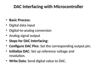
DAC Interfacing withMicrocontroller
• Basic Process:
• Digital data input
• Digital-to-analog conversion
• Analog signal output
• Steps for DAC Interfacing:
• Configure DAC Pins: Set the corresponding output pin.
• Initialize DAC: Set up reference voltage and
resolution.
• Write Data: Send digital value to DAC.
8.
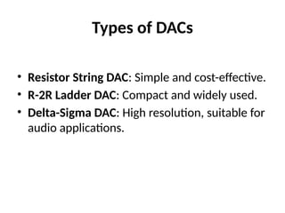
Types of DACs
•Resistor String DAC: Simple and cost-effective.
• R-2R Ladder DAC: Compact and widely used.
• Delta-Sigma DAC: High resolution, suitable for
audio applications.
9.
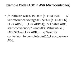
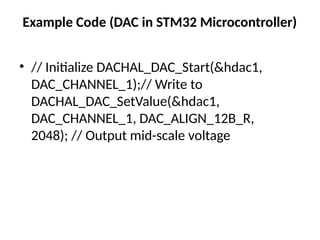
Example Code (DACin STM32 Microcontroller)
• // Initialize DACHAL_DAC_Start(&hdac1,
DAC_CHANNEL_1);// Write to
DACHAL_DAC_SetValue(&hdac1,
DAC_CHANNEL_1, DAC_ALIGN_12B_R,
2048); // Output mid-scale voltage
10.
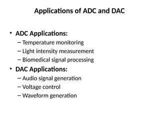
Applications of ADCand DAC
• ADC Applications:
– Temperature monitoring
– Light intensity measurement
– Biomedical signal processing
• DAC Applications:
– Audio signal generation
– Voltage control
– Waveform generation
11.
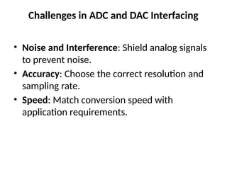
Challenges in ADCand DAC Interfacing
• Noise and Interference: Shield analog signals
to prevent noise.
• Accuracy: Choose the correct resolution and
sampling rate.
• Speed: Match conversion speed with
application requirements.
12.
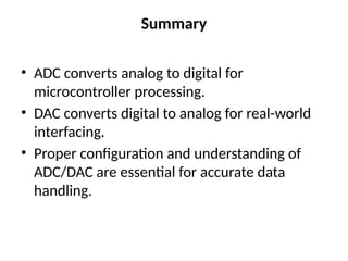
Summary
• ADC convertsanalog to digital for
microcontroller processing.
• DAC converts digital to analog for real-world
interfacing.
• Proper configuration and understanding of
ADC/DAC are essential for accurate data
handling.
13.
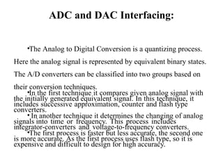
ADC and DACInterfacing:
•The Analog to Digital Conversion is a quantizing process.
Here the analog signal is represented by equivalent binary states.
The A/D converters can be classified into two groups based on
their conversion techniques.
•In the first technique it compares given analog signal with
the initially generated equivalent signal. In this technique, it
includes successive approximation, counter and flash type
converters.
• In another technique it determines the changing of analog
signals into time or frequency. This process includes
integrator-converters and voltage-to-frequency converters.
•The first process is faster but less accurate, the second one
is more accurate. As the first process uses flash type, so it is
expensive and difficult to design for high accuracy.
14.
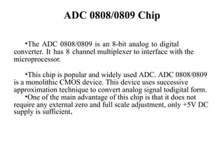
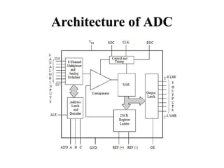
ADC 0808/0809 Chip
•TheADC 0808/0809 is an 8-bit analog to digital
converter. It has 8 channel multiplexer to interface with the
microprocessor.
•This chip is popular and widely used ADC. ADC 0808/0809
is a monolithic CMOS device. This device uses successive
approximation technique to convert analog signal todigital form.
•One of the main advantage of this chip is that it does not
require any external zero and full scale adjustment, only +5V DC
supply is sufficient.
15.
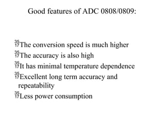
Good features ofADC 0808/0809:
The conversion speed is much higher
The accuracy is also high
It has minimal temperature dependence
Excellent long term accuracy and
repeatability
Less power consumption
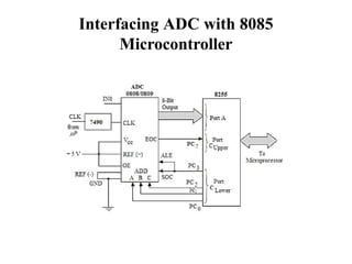
• The PortAof 8255 chip is used as the input port. The PC7 pin of
Port Cupper is connected to the End of Conversion (EOC) Pin of the
analog to digital converter. This port is also used as input port.
• The Clower port is used as output port. The PC2-0 lines are
connected to three address pins of this chip to select input channels.
The PC3 pin is connected to the Start of Conversion (SOC) pin and
ALE pin of ADC 0808/0809.
•Now let us see a program to generate digital signal from analog data.
We are using IN0 as input pin, so the pin selection value will be 00H
19.
PROGRAM
•MVI A, 98H; Set Port A and Cupper as input, CLower as output OUT 03H ;
Write control word 8255-I to control Wordregister XRA A ; Clear the accumulator
•OUT 02H ; Send the content of Acc to Port Clower to select IN0
•MVI A, 08H ; Load the accumulator with 08H OUT 02H ; ALE and SOC
will be 0
•XRA A ; Clear the accumulator
•OUT 02H ; ALE and SOC will be low. READ: IN 02H ; Read from
EOC (PC7)
•RAL ; Rotate left to check C7 is 1.
•JNC READ ; If C7 is not 1, go to READ IN 00H ; Read digital output
of ADC STA 8000H ; Save result at 8000H
•HLT ; Stop the program
20.
DIGITAL-TO-ANALOG (DAC) CONVERTER:
•Thetwo method of creating a DAC is binary weighted and R/2R ladder.
• The Binary Weighted DAC, which contains one resistor or current
source for each bit of the DAC connected to a summing point. These
precise voltages or currents sum to the correct output value. This is one
of the fastest conversion methods but suffers from poor accuracy
because of the high precision required for each individual voltage or
current. Such high-precision resistors and current-sources are expensive,
so this type of converter is usually limited to 8-bit resolution or less
21.
R-2R ladder DAC
•The R-2R ladder DAC, which is a binary
weighted DAC that uses a repeating cascaded
structure of resistor values R and 2R. This
improves the precision due to the relative ease
of producing equal valued matched resistors
(or current sources). However, wide converters
perform slowly due to increasingly large RC-
constants for each added R-2R link.
22.
DAC Contd..
• Thefirst criterion for judging a DAC is its resolution,
which is a function of the number of binary inputs. The
common ones are 8, 10, and 12 bits.
• The number of data bit inputs decides the resolution of the
DAC since the number of analog output levels is equal to
2n, where n is the number of data bit inputs. Therefore, an
8-input DAC such as the DAC0808 provides 256 discrete
voltage (or current) levels of output.
• Similarly, the 12-bit DAC provides 4096 discrete voltage
levels. There also 16-bit DACs, but they are more
expensive
23.
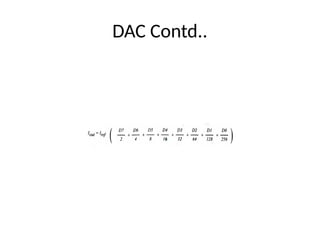
DAC Contd..
➢The digitalinputs are converter to current (Iout), and
by connecting a resistor to the Iout pin, we can convert the
result to voltage.
➢The total current provided by the Iout pin is a function
of the binary numbers at the D0-D7 inputs of the
DAC0808 and the reference current (Iref), and is as
follows
DAC Contd..
•Usually referencecurrent is 2mA.
➢
Ideally, we connect the output pin to a resistor, convert this
current to voltage, and monitor the output on the scope.
➢
But this can cause inaccuracy; hence an opamp is used to convert
the output current to voltage.
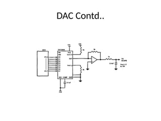
➢The 8051 connection to DAC0808is as shown in the below Figure
5.5.4.
➢
Now assuming that Iref = 2mA, if all the inputs to the DAC are
high, the maximum output current is 1.99mA.
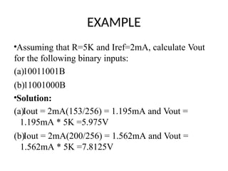
EXAMPLE
•Assuming that R=5Kand Iref=2mA, calculate Vout
for the following binary inputs:
(a)10011001B
(b)11001000B
•Solution:
(a)Iout = 2mA(153/256) = 1.195mA and Vout =
1.195mA * 5K =5.975V
(b)Iout = 2mA(200/256) = 1.562mA and Vout =
1.562mA * 5K =7.8125V
28.
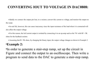
CONVERTING IOUT TOVOLTAGE IN DAC0808:
➢Ideally we connect the output pin lout, to a resistor, convert this current to voltage, and monitor the output on
the scope.
➢In real life, however, this can cause inaccuracy since the input resistance of the load where it is connected will
also affect the output voltage.
➢For this reason, the lref current output is isolated by connecting it to an op-amp such as the 741 with Rf = 5K
ohms for the feedback resistor.
➢Assuming that R= 5K ohms, by changing the binary input, the output voltage changes as shown in Example 2.
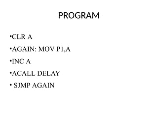
•Example 2:
•In order to generate a stair-step ramp, set up the circuit in
Figure and connect the output to an oscilloscope. Then write a
program to send data to the DAC to generate a stair-step ramp.