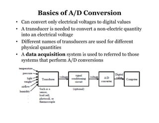
Lecture 13
ADC Interfacing
Fall 2014
Armaghan Mohsin
Department of Physics
CIIT Islamabad
Real Time
Embedded Systems
EEE446
Basics of A/D Conversion
• Can convert only electrical voltages to digital values
• A transducer is needed to convert a non-electric quantity
into an electrical voltage
• Different names of transducers are used for different
physical quantities
• A data acquisition system is used to referred to those
systems that perform A/D conversions
Analog Voltage and Digital Code
• Characteristic of an Ideal A/D Converter
– Needs infinite number of bits to encode the A/D
conversion result
– Unachievable and impractical
Characteristic of an Ideal n-bit ADC
• The area between dotted line and staircase is called the
quantization error.
– The resolution of this A/D converter is VDD/2n.
– Average conversion error is VDD/2n+1.
– A real A/D converter has nonlinearity
Optimal Voltage Range for ADC
• A/D converter requires a low reference voltage (VREF-)
and a high reference voltage (VREF+) to perform
conversion.
– Most A/D converters are ratiomertic:
• An analog input of VREF- is converted to digital code 0.
• An analog input of VREF+ is converted to digital code 2n-1.
• An analog input of k V is converted to digital code k
• The A/D conversion result k corresponds to the following
analog input:
VK = VREF- +((VREF+ - VREF-) * k) ÷ (2n – 1)
• Most systems use VDD and 0V as VREF+ and VREF-,
respectively.
• The output of a transducer should be scaled and shifted
to the range of 0V ~ VDD in order to achieve the best
accuracy
Example
Suppose that there is a 10-bit A/D converter with VREF- =
1 V and VREF+ = 4V. Find the corresponding voltage values
for the A/D conversion results of 25, 80, 240, and 900.
Solution:
VK = VREF- +((VREF+ - VREF-) * k) ÷ (2n – 1)
The corresponding voltages are as follows:
1V + (3 * 25) ÷ (210 – 1) = 1.07 V
1V + (3 * 80) ÷ (210 – 1) = 1.23 V
1V + (3 * 240) ÷ (210 – 1) = 1.70 V
1V + (3 * 900) ÷ (210 – 1) = 3.64 V
PIC18F ADC Module
• The PIC18 has a 10-bit A/D converter.
– The number of analog inputs varies among difference
PIC18 devices.
– The A/D converter has the following registers:
• A/D Result High Register (ADRESH)
• A/D Result Low Register (ADRESL)
• A/D Control Register 0 (ADCON0)
• A/D Control Register 1 (ADCON1)
• A/D Control Register 2 (ADCON2)
• The contents of these registers vary with the PIC18 members.
– Early PIC18 (PIC18FXX2) members have only ADCON0
and ADCON1 registers.
ADCON0 Register
ADCON1 Register
ADCON2 Register
Successive Approximation
• The A/D converters in most PICmicro MCUs are of the
Successive Approximation type
• Converts one bit at a time
• Converts MSB first, LSB last
• One A/D clock time required for each bit
Conversion Time
• Each bit requires one A/D clock period (TAD) for
conversion
• Two to three additional A/D clocks required for settling
time
• After conversion the final value is written to the result
register
A/D Clock
• Multiple Sources
– 2TOSC (FOSC/2)
– 8TOSC (FOSC/8)
– 32TOSC (FOSC/32)
– RC (dedicated internal) 4 or 6uS typical
• Must meet minimum time
A/D Conversion Steps
• Configure I/O Pins
• Select the Channel to Convert
• Configure and Enable the A/D
• Wait the Acquisition Time
• Initiate the Conversion
• Wait for the Conversion to Complete
• Read the Result

ADC Interfacing with pic Microcontrollert

  • 1.
    Lecture 13 ADC Interfacing Fall2014 Armaghan Mohsin Department of Physics CIIT Islamabad Real Time Embedded Systems EEE446
  • 2.
    Basics of A/DConversion • Can convert only electrical voltages to digital values • A transducer is needed to convert a non-electric quantity into an electrical voltage • Different names of transducers are used for different physical quantities • A data acquisition system is used to referred to those systems that perform A/D conversions
  • 3.
    Analog Voltage andDigital Code • Characteristic of an Ideal A/D Converter – Needs infinite number of bits to encode the A/D conversion result – Unachievable and impractical
  • 4.
    Characteristic of anIdeal n-bit ADC • The area between dotted line and staircase is called the quantization error. – The resolution of this A/D converter is VDD/2n. – Average conversion error is VDD/2n+1. – A real A/D converter has nonlinearity
  • 5.
    Optimal Voltage Rangefor ADC • A/D converter requires a low reference voltage (VREF-) and a high reference voltage (VREF+) to perform conversion. – Most A/D converters are ratiomertic: • An analog input of VREF- is converted to digital code 0. • An analog input of VREF+ is converted to digital code 2n-1. • An analog input of k V is converted to digital code k • The A/D conversion result k corresponds to the following analog input: VK = VREF- +((VREF+ - VREF-) * k) ÷ (2n – 1) • Most systems use VDD and 0V as VREF+ and VREF-, respectively. • The output of a transducer should be scaled and shifted to the range of 0V ~ VDD in order to achieve the best accuracy
  • 6.
    Example Suppose that thereis a 10-bit A/D converter with VREF- = 1 V and VREF+ = 4V. Find the corresponding voltage values for the A/D conversion results of 25, 80, 240, and 900. Solution: VK = VREF- +((VREF+ - VREF-) * k) ÷ (2n – 1) The corresponding voltages are as follows: 1V + (3 * 25) ÷ (210 – 1) = 1.07 V 1V + (3 * 80) ÷ (210 – 1) = 1.23 V 1V + (3 * 240) ÷ (210 – 1) = 1.70 V 1V + (3 * 900) ÷ (210 – 1) = 3.64 V
  • 7.
    PIC18F ADC Module •The PIC18 has a 10-bit A/D converter. – The number of analog inputs varies among difference PIC18 devices. – The A/D converter has the following registers: • A/D Result High Register (ADRESH) • A/D Result Low Register (ADRESL) • A/D Control Register 0 (ADCON0) • A/D Control Register 1 (ADCON1) • A/D Control Register 2 (ADCON2) • The contents of these registers vary with the PIC18 members. – Early PIC18 (PIC18FXX2) members have only ADCON0 and ADCON1 registers.
  • 8.
  • 9.
  • 10.
  • 11.
    Successive Approximation • TheA/D converters in most PICmicro MCUs are of the Successive Approximation type • Converts one bit at a time • Converts MSB first, LSB last • One A/D clock time required for each bit
  • 12.
    Conversion Time • Eachbit requires one A/D clock period (TAD) for conversion • Two to three additional A/D clocks required for settling time • After conversion the final value is written to the result register
  • 13.
    A/D Clock • MultipleSources – 2TOSC (FOSC/2) – 8TOSC (FOSC/8) – 32TOSC (FOSC/32) – RC (dedicated internal) 4 or 6uS typical • Must meet minimum time
  • 14.
    A/D Conversion Steps •Configure I/O Pins • Select the Channel to Convert • Configure and Enable the A/D • Wait the Acquisition Time • Initiate the Conversion • Wait for the Conversion to Complete • Read the Result