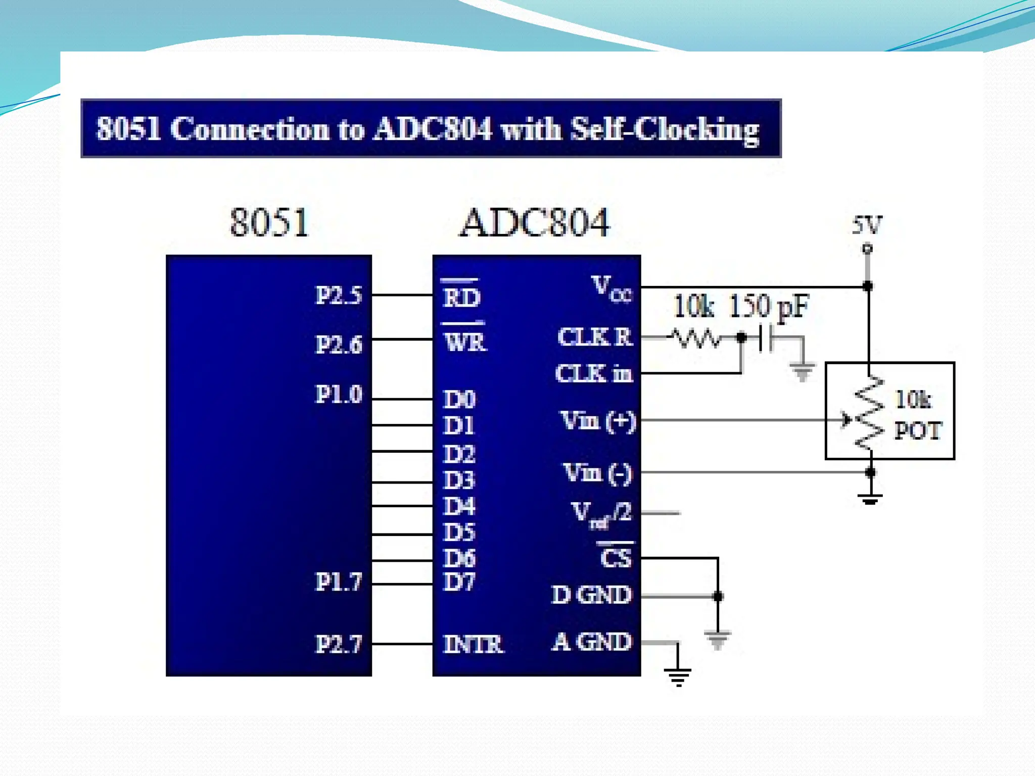
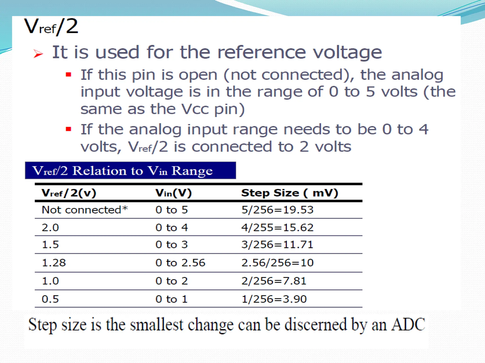
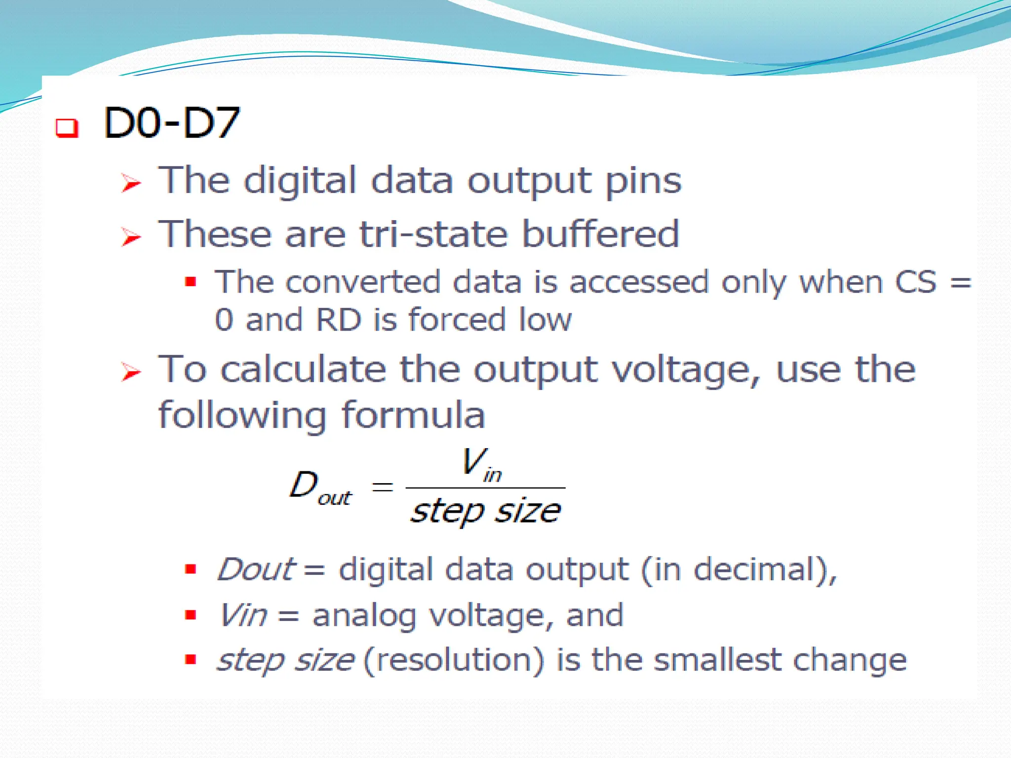
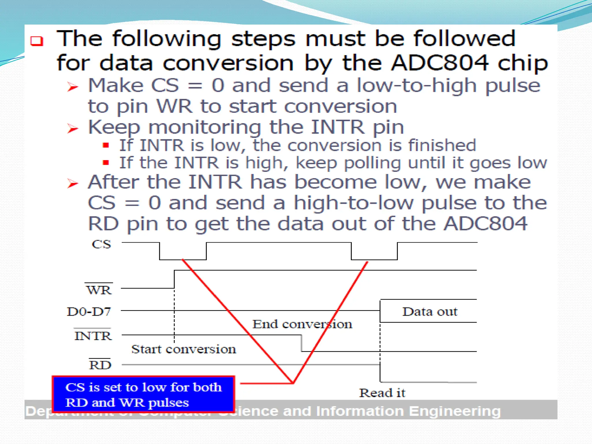
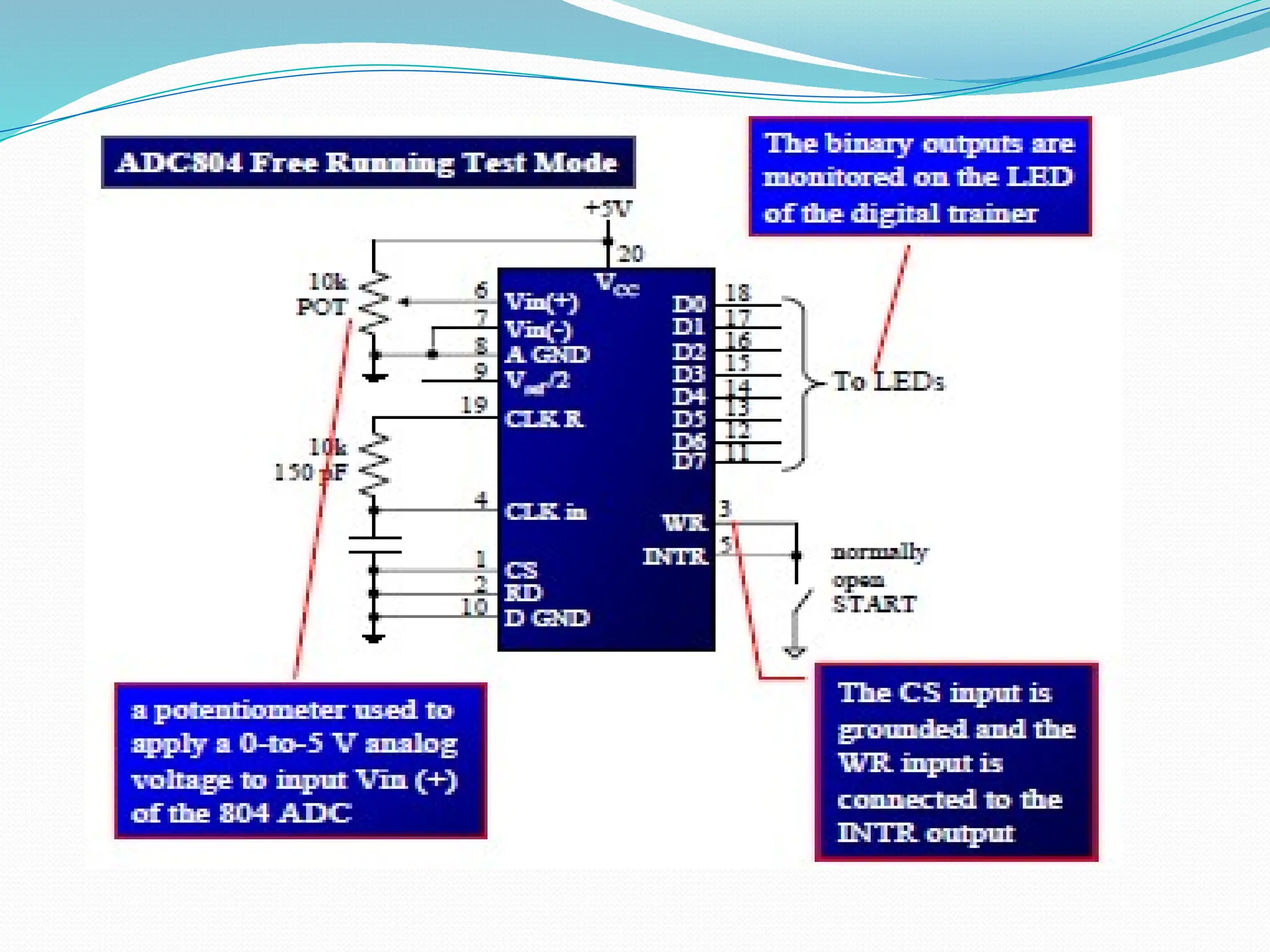
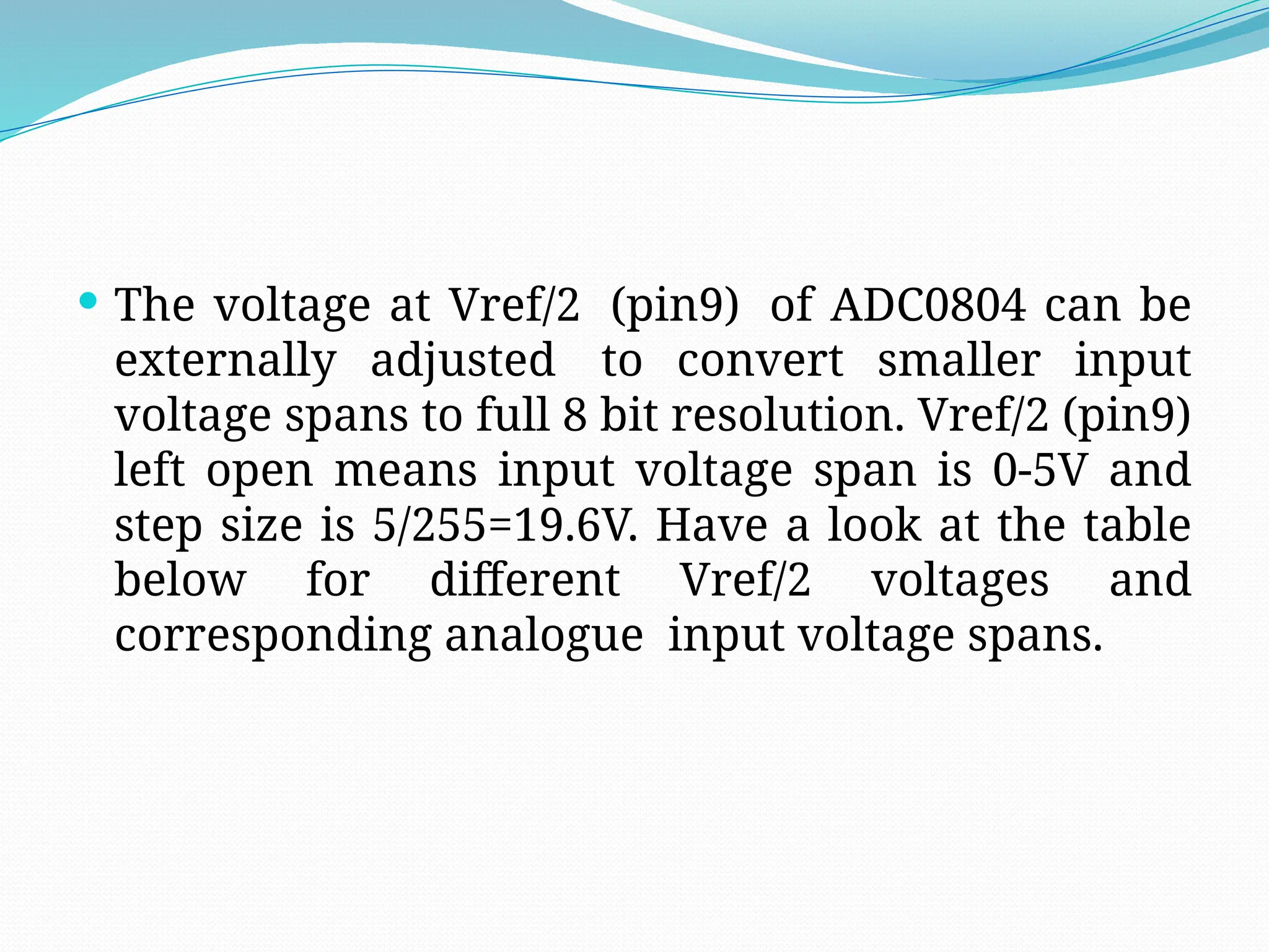
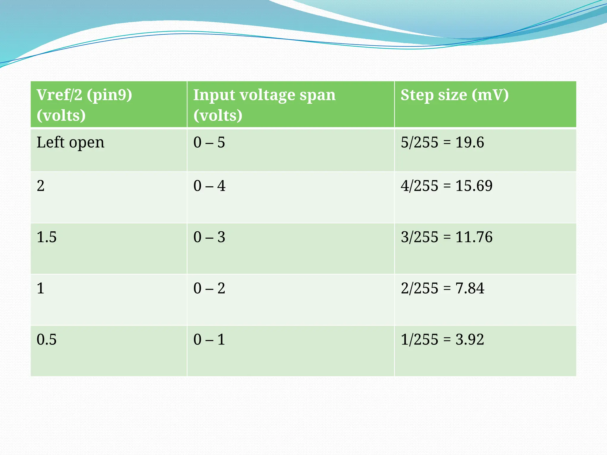
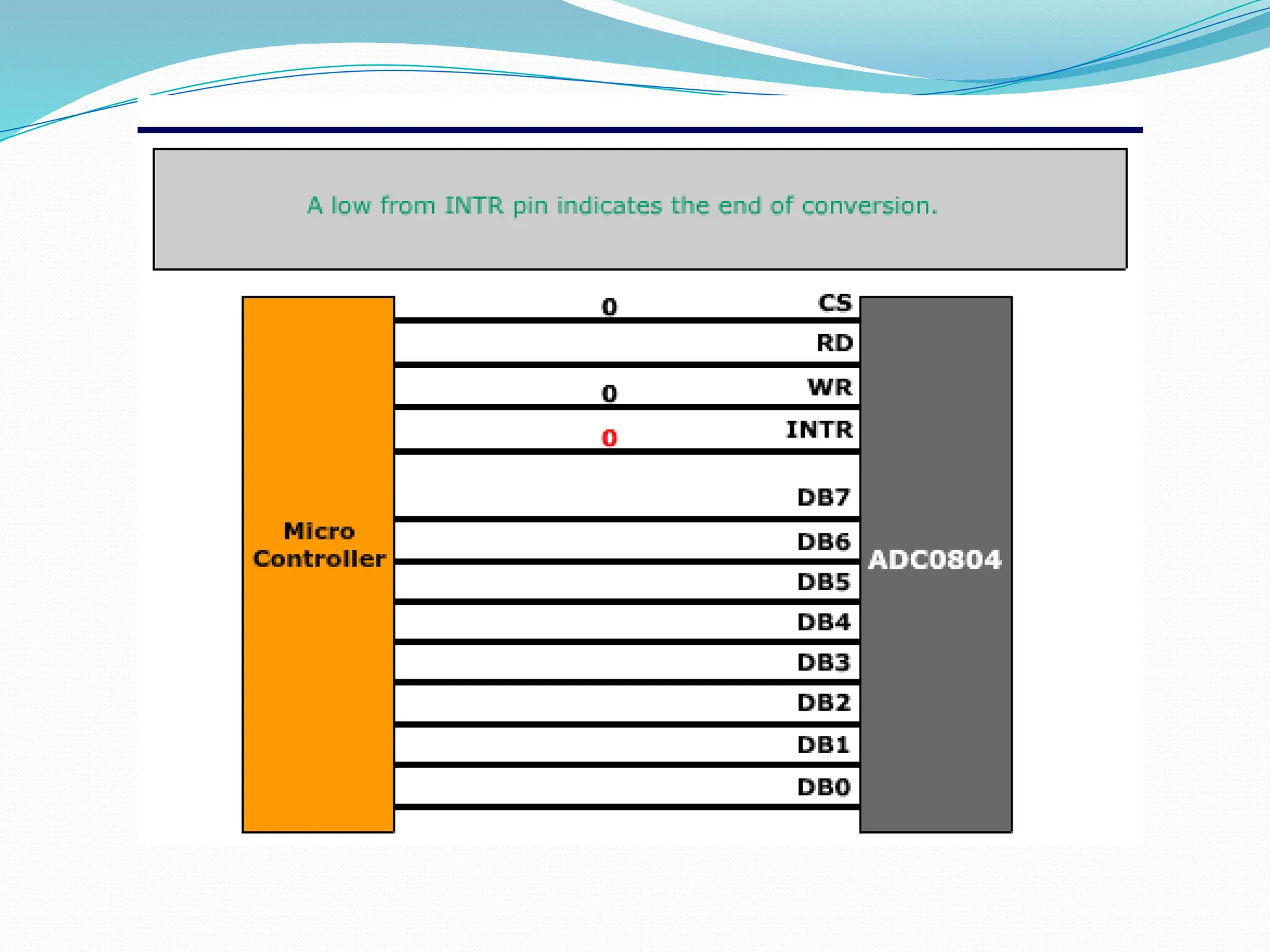
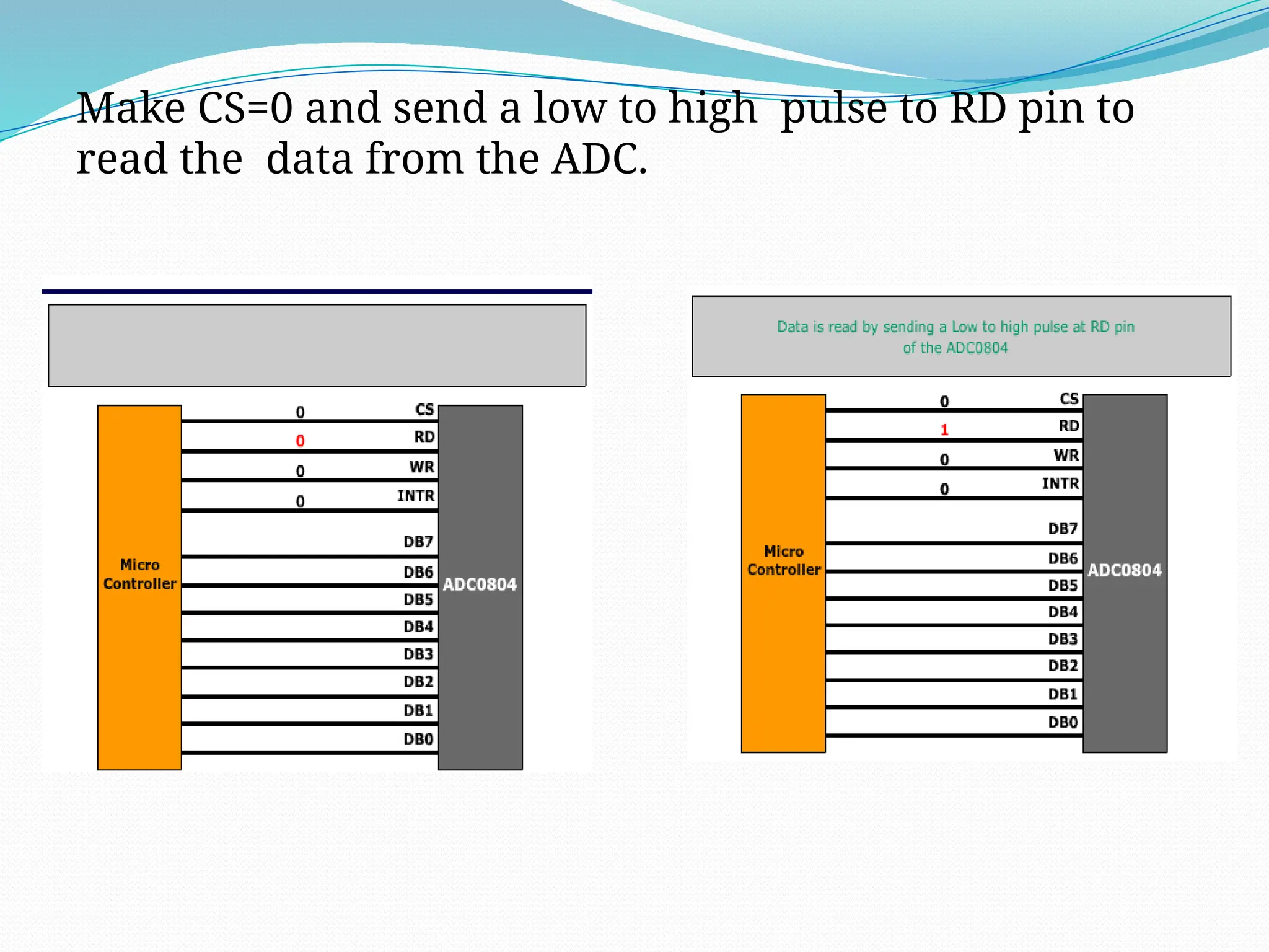
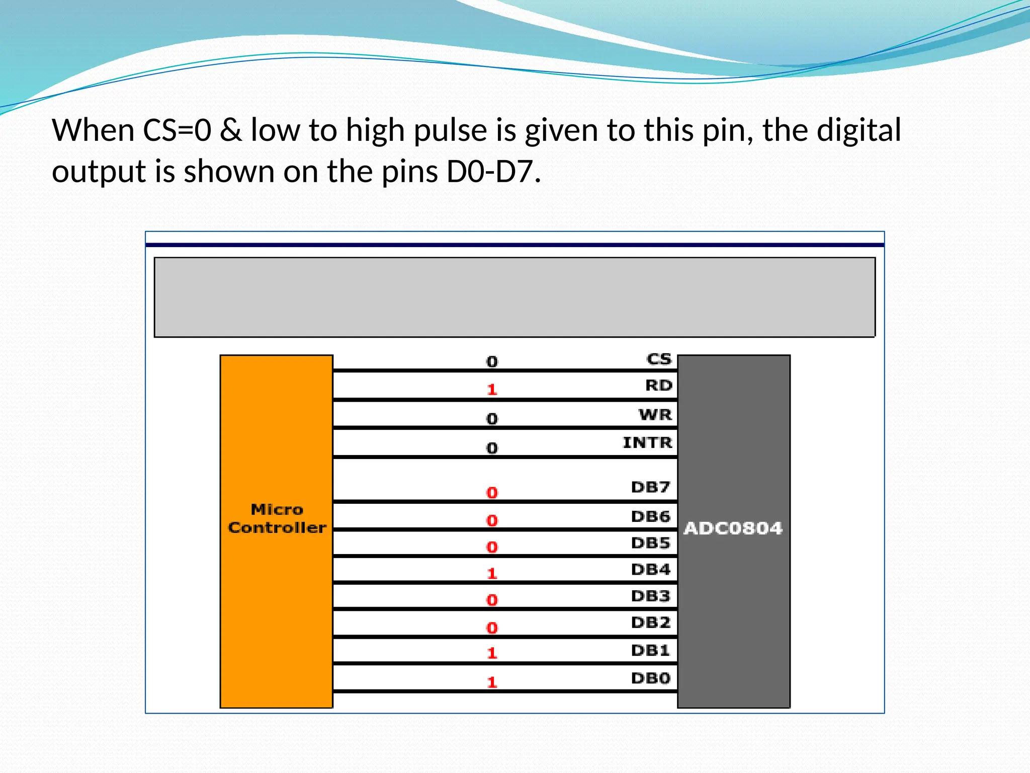
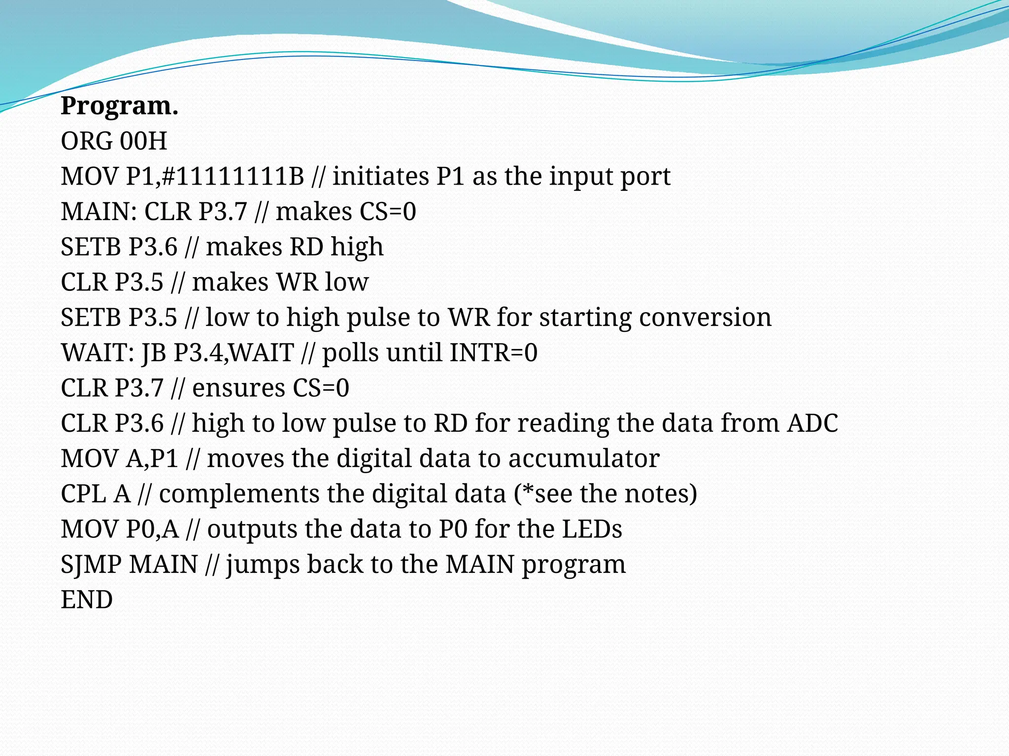
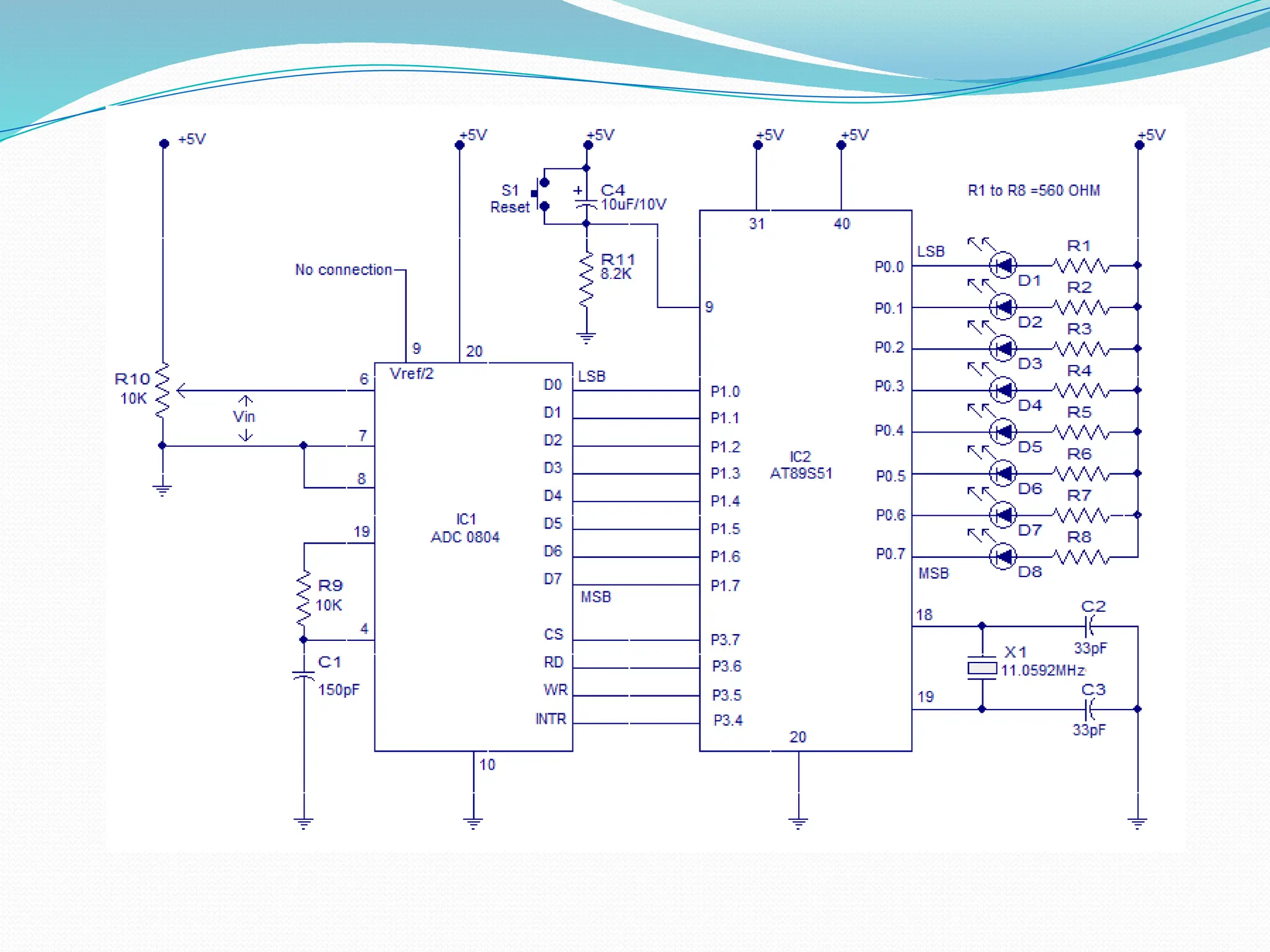
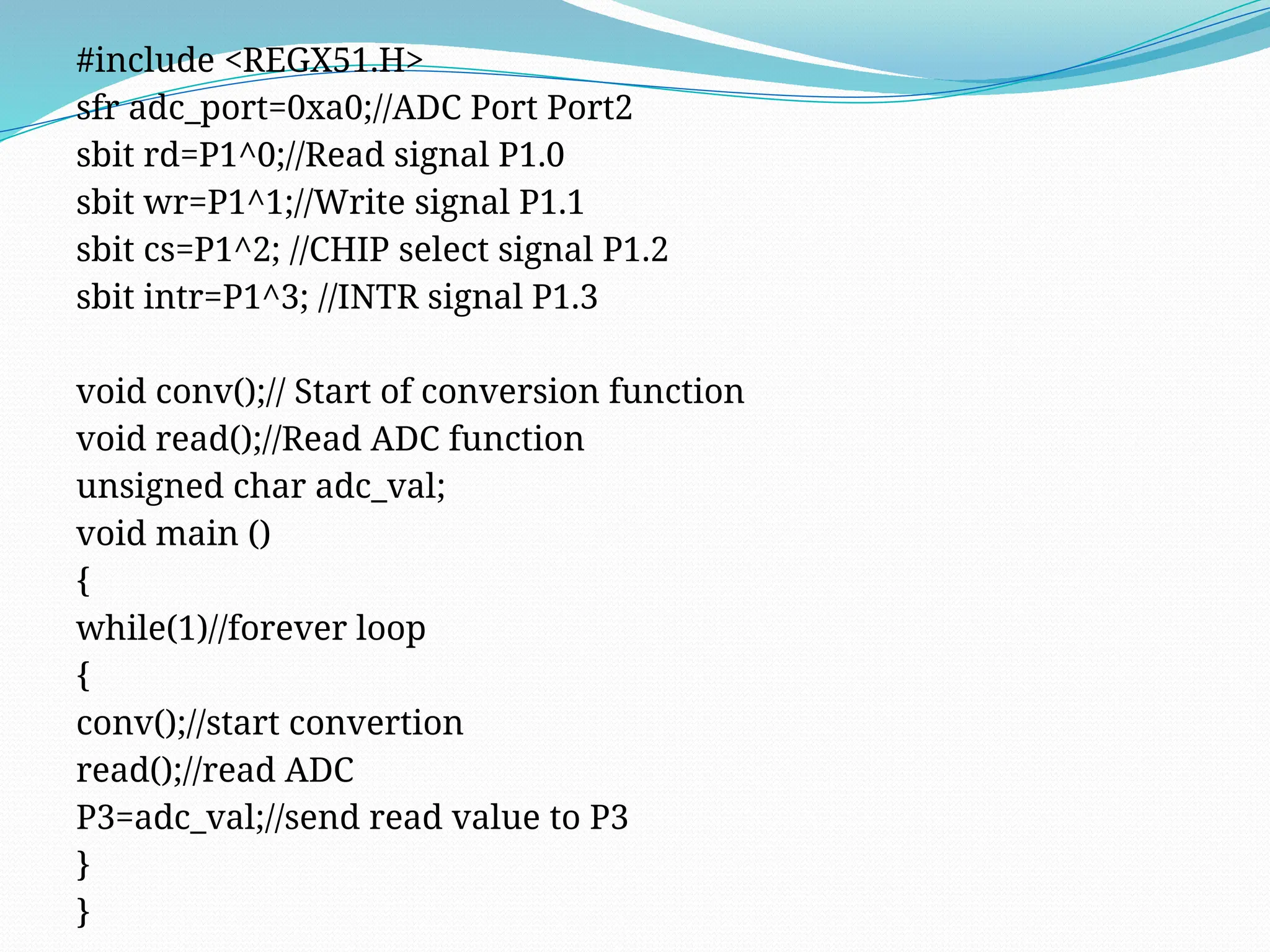
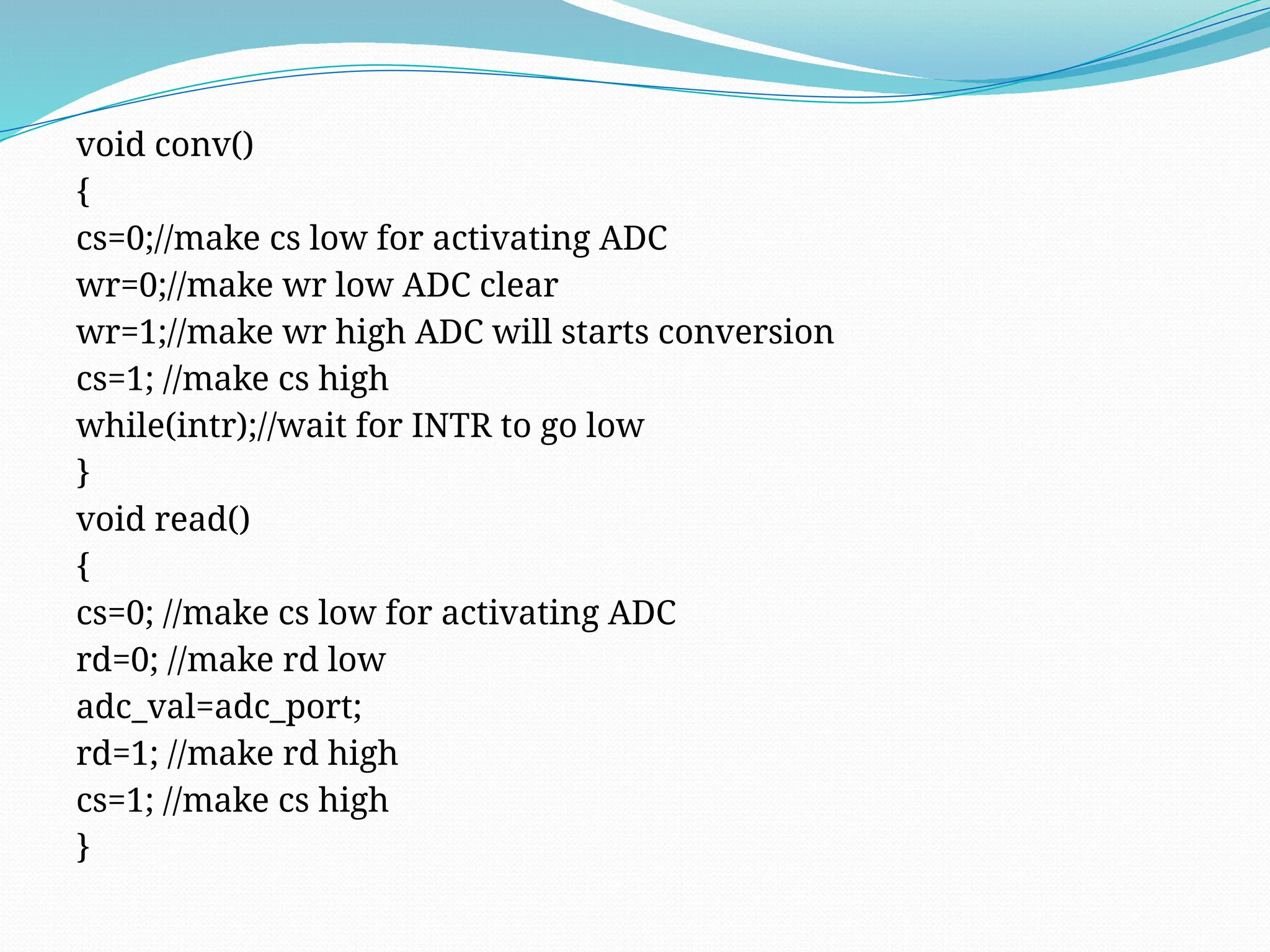
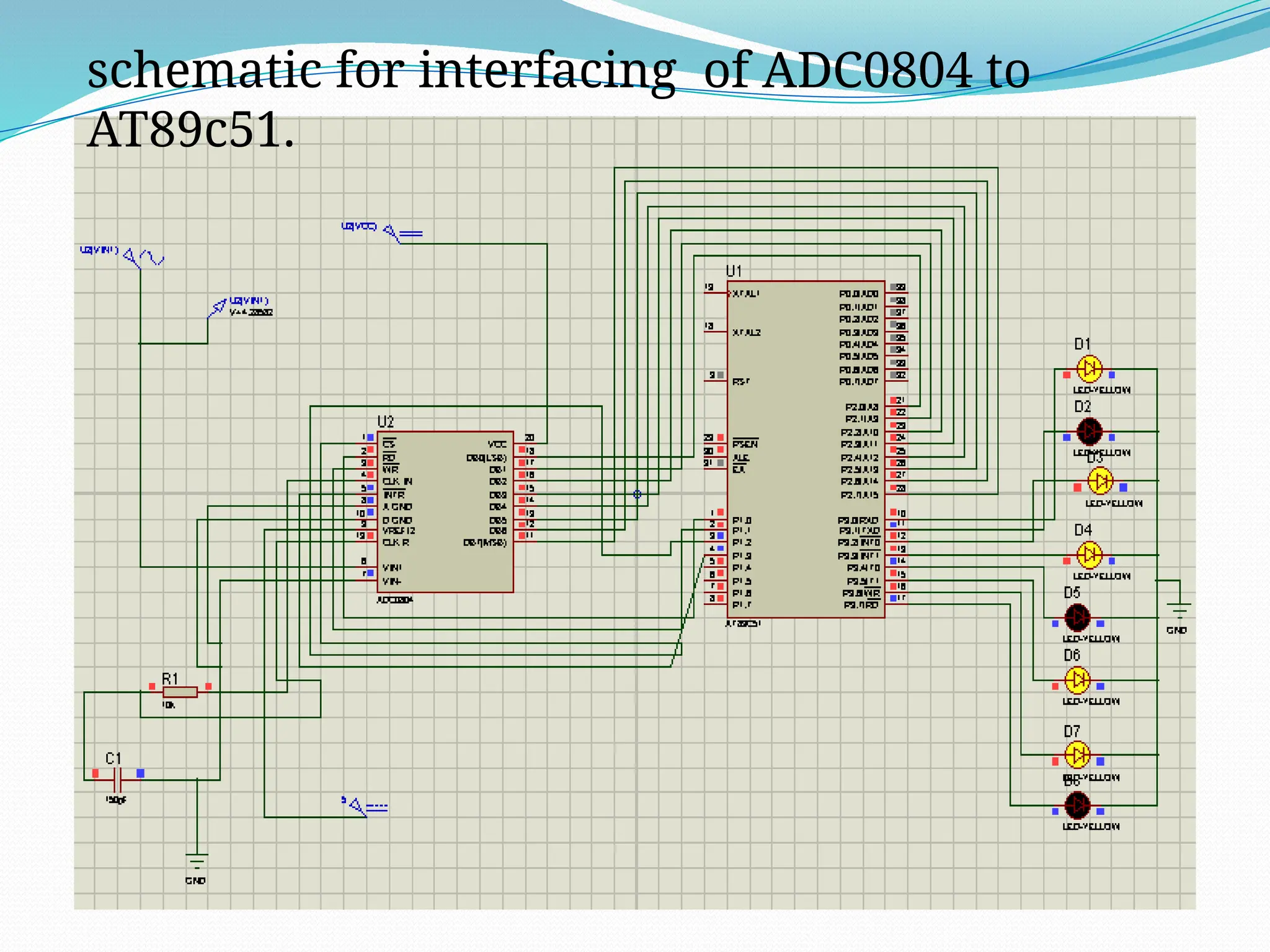
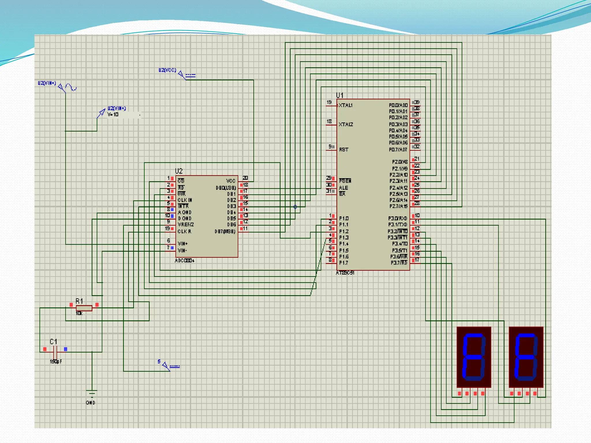
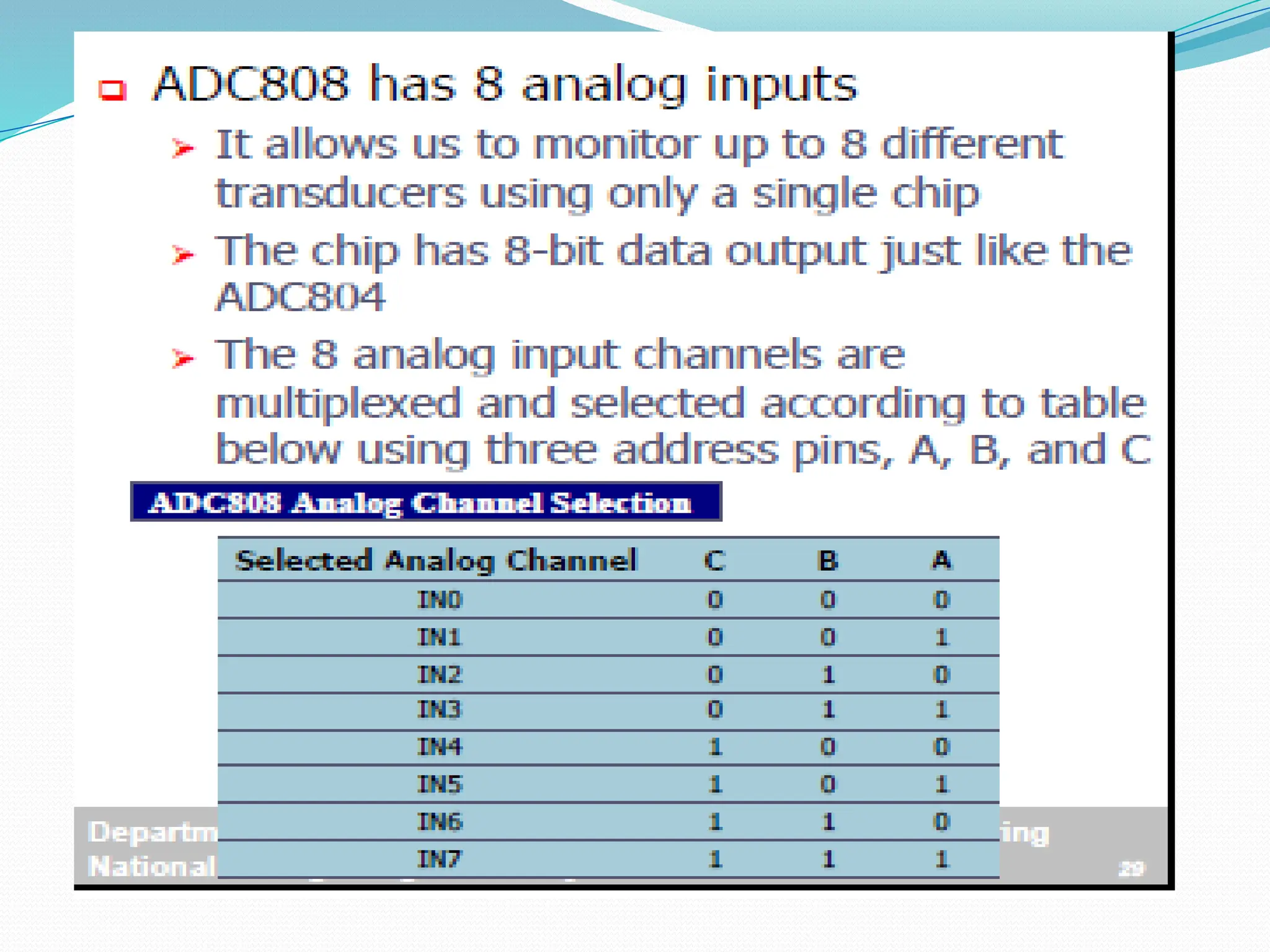
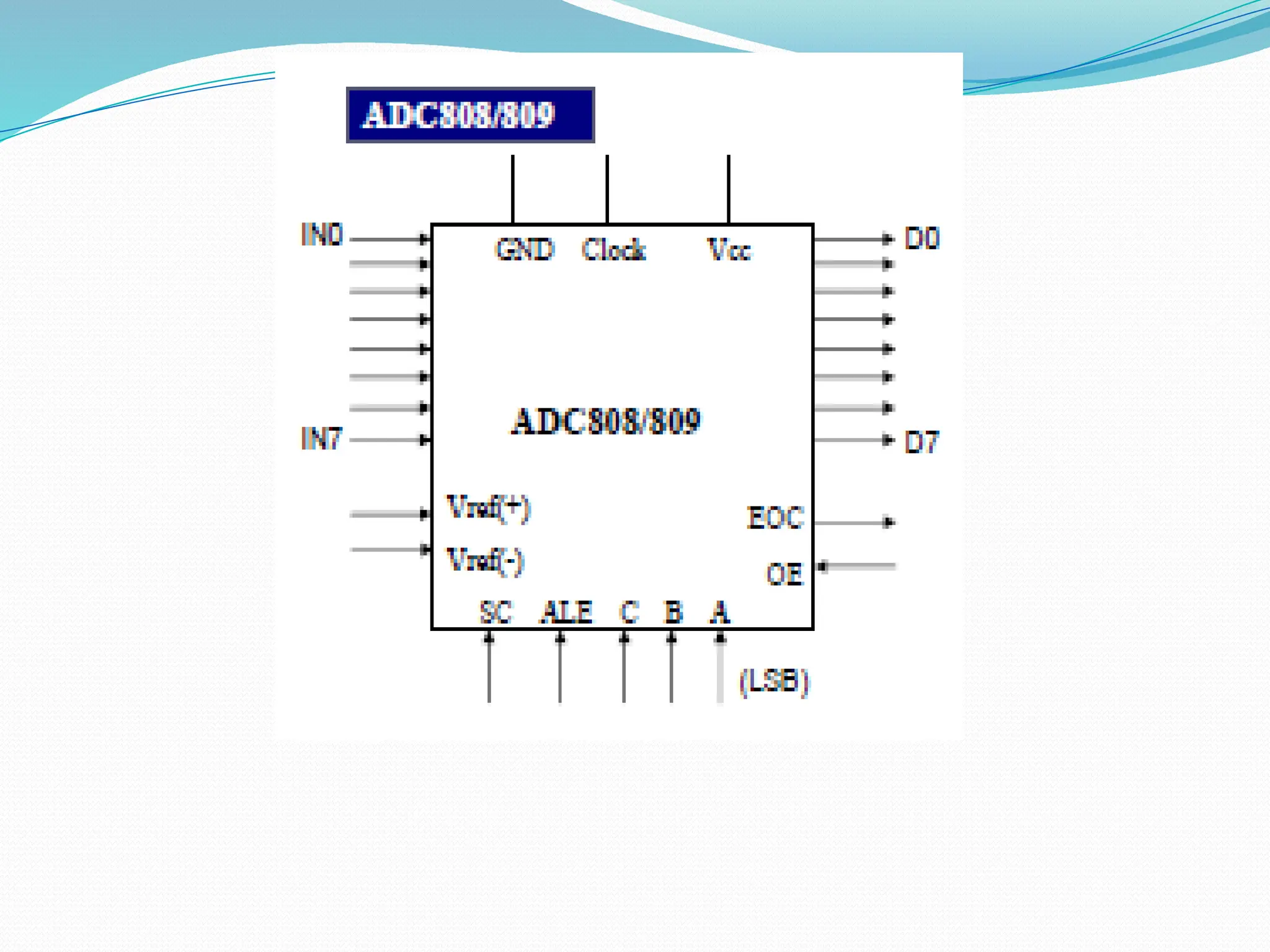
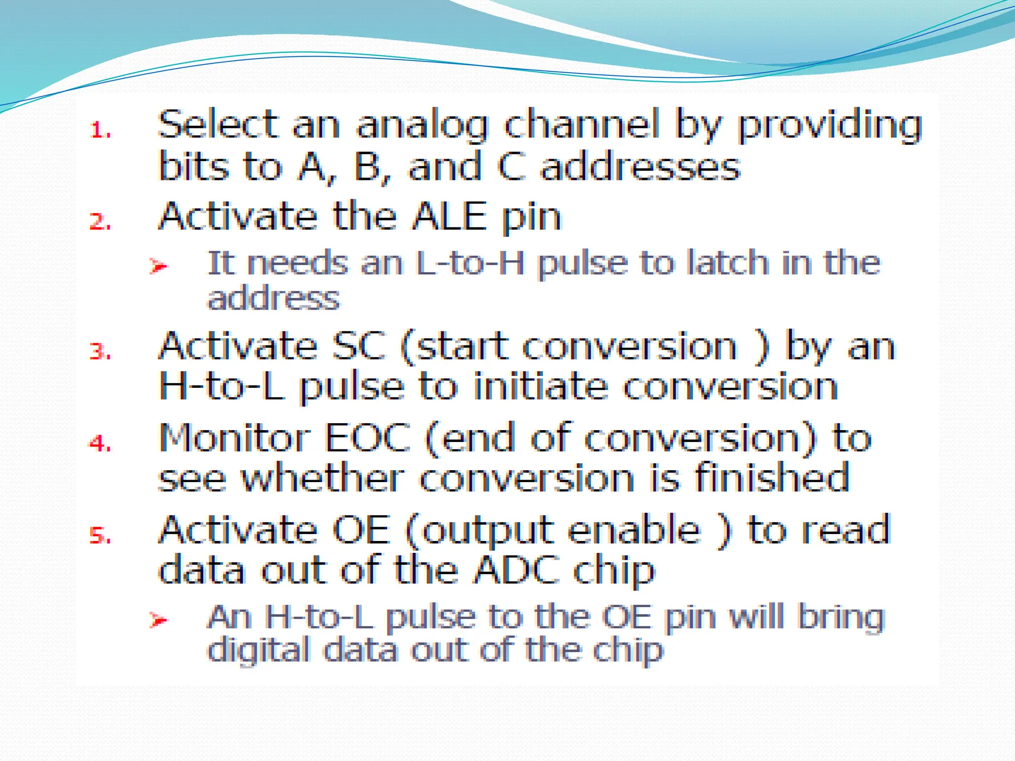
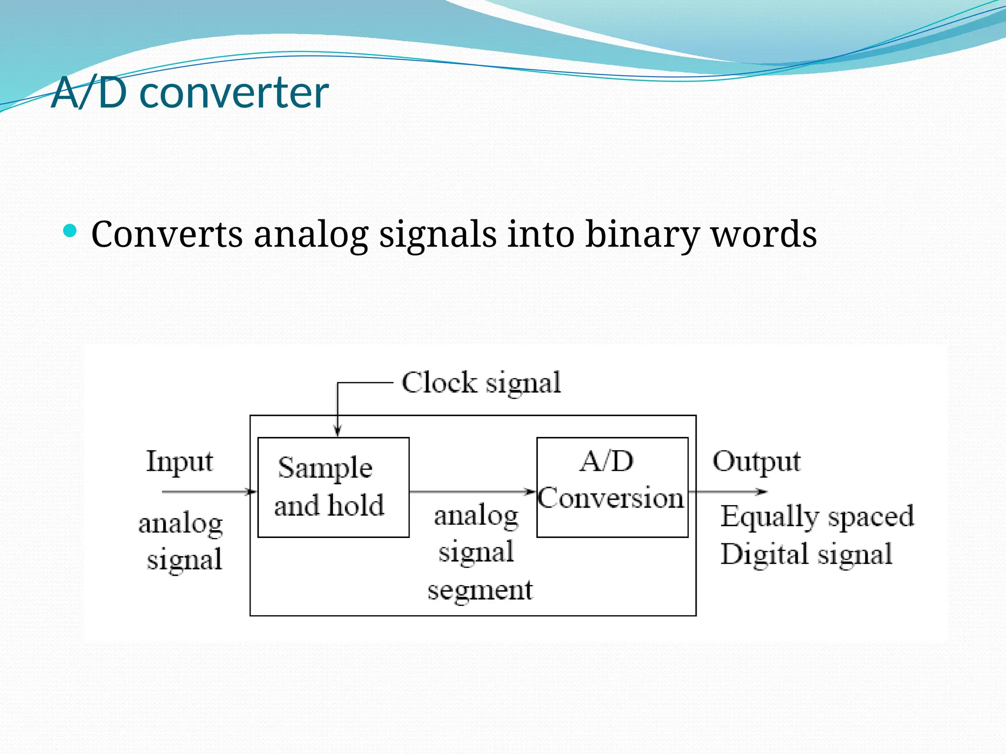
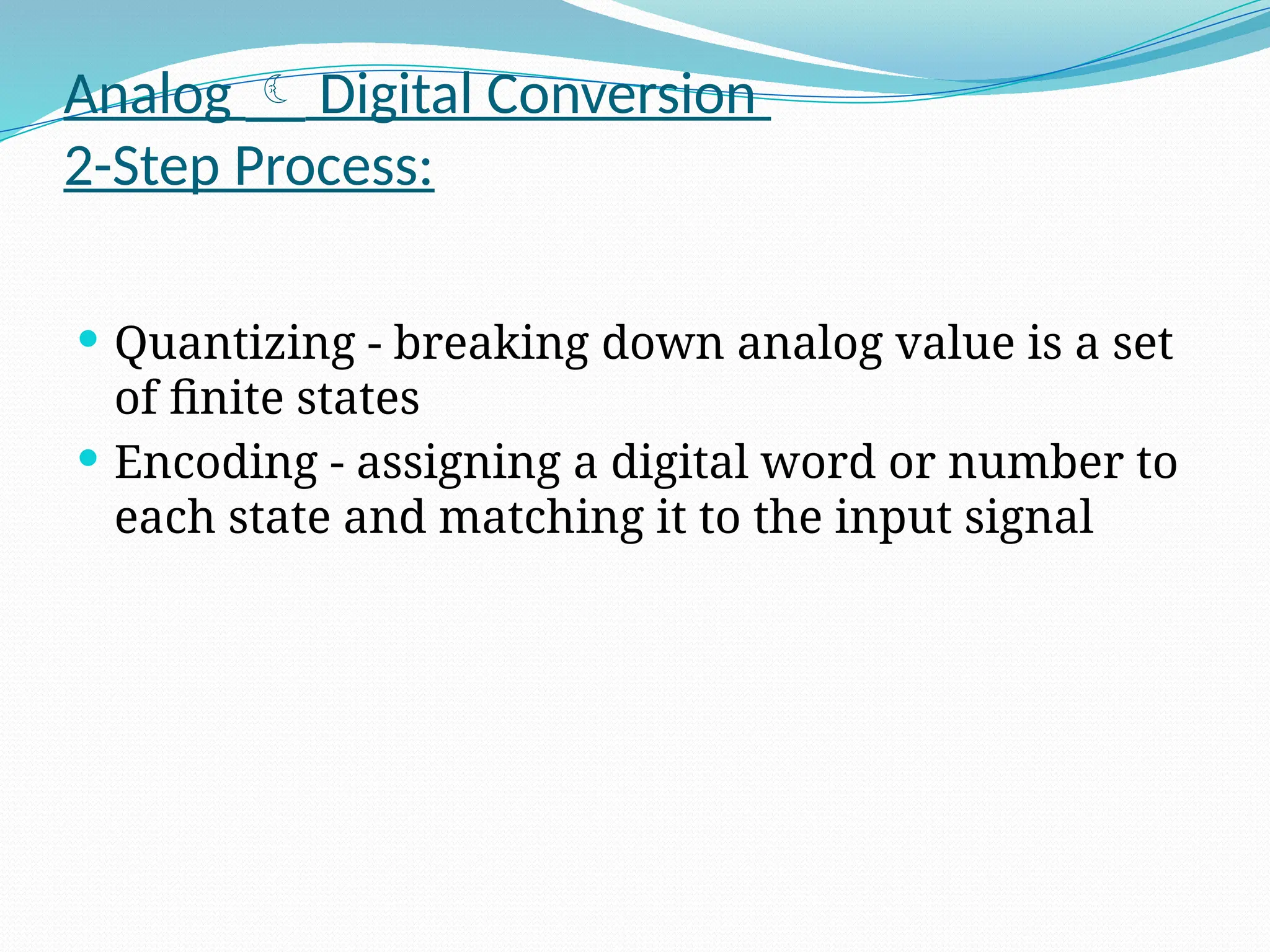
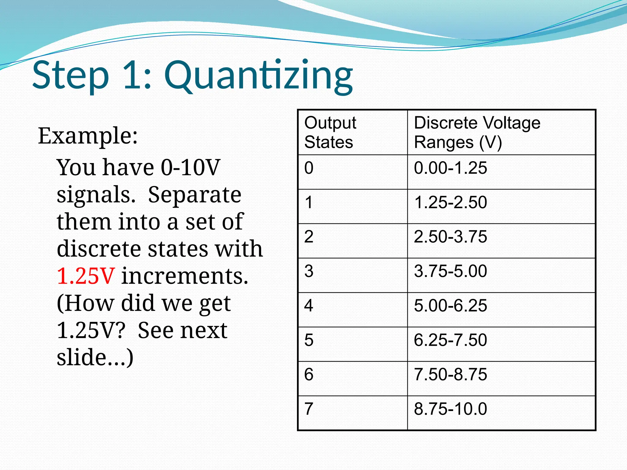
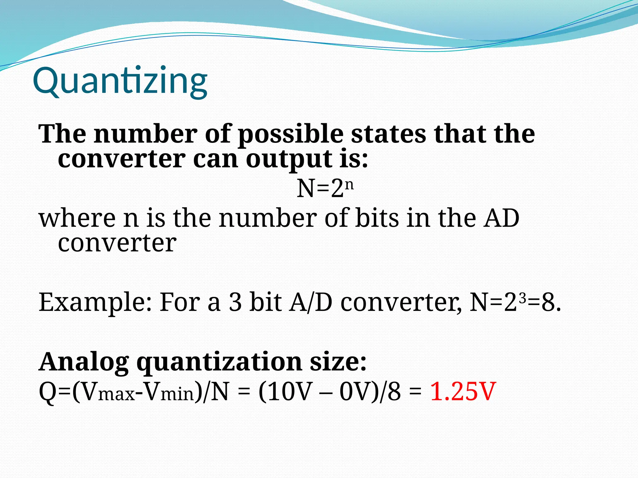
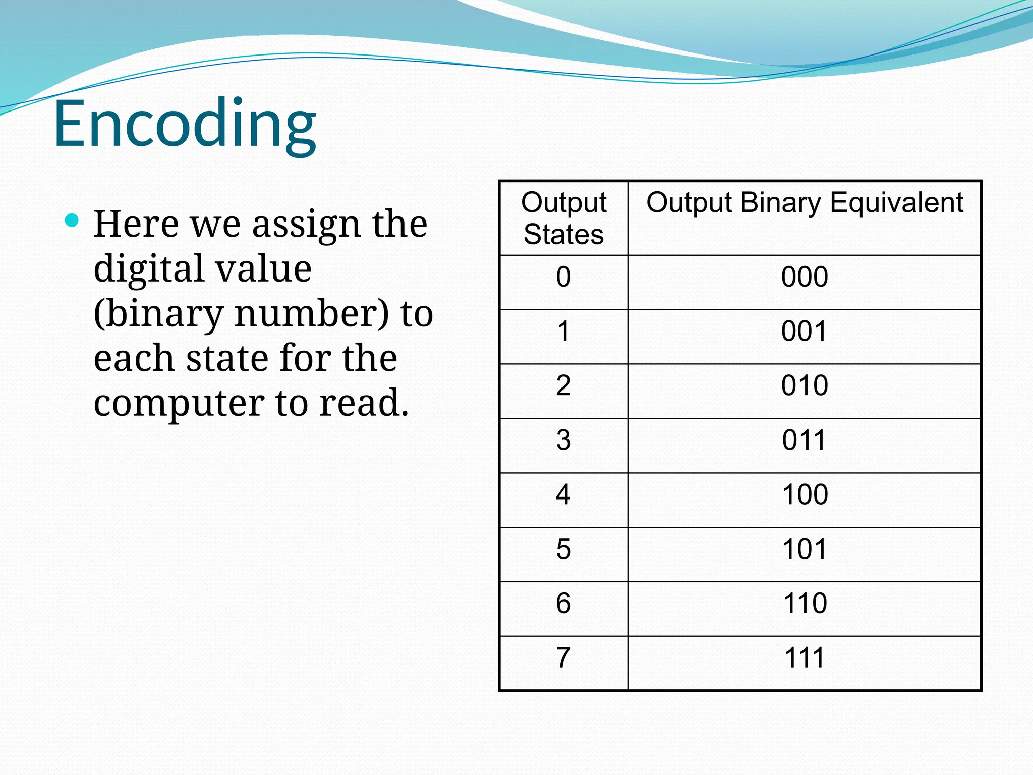
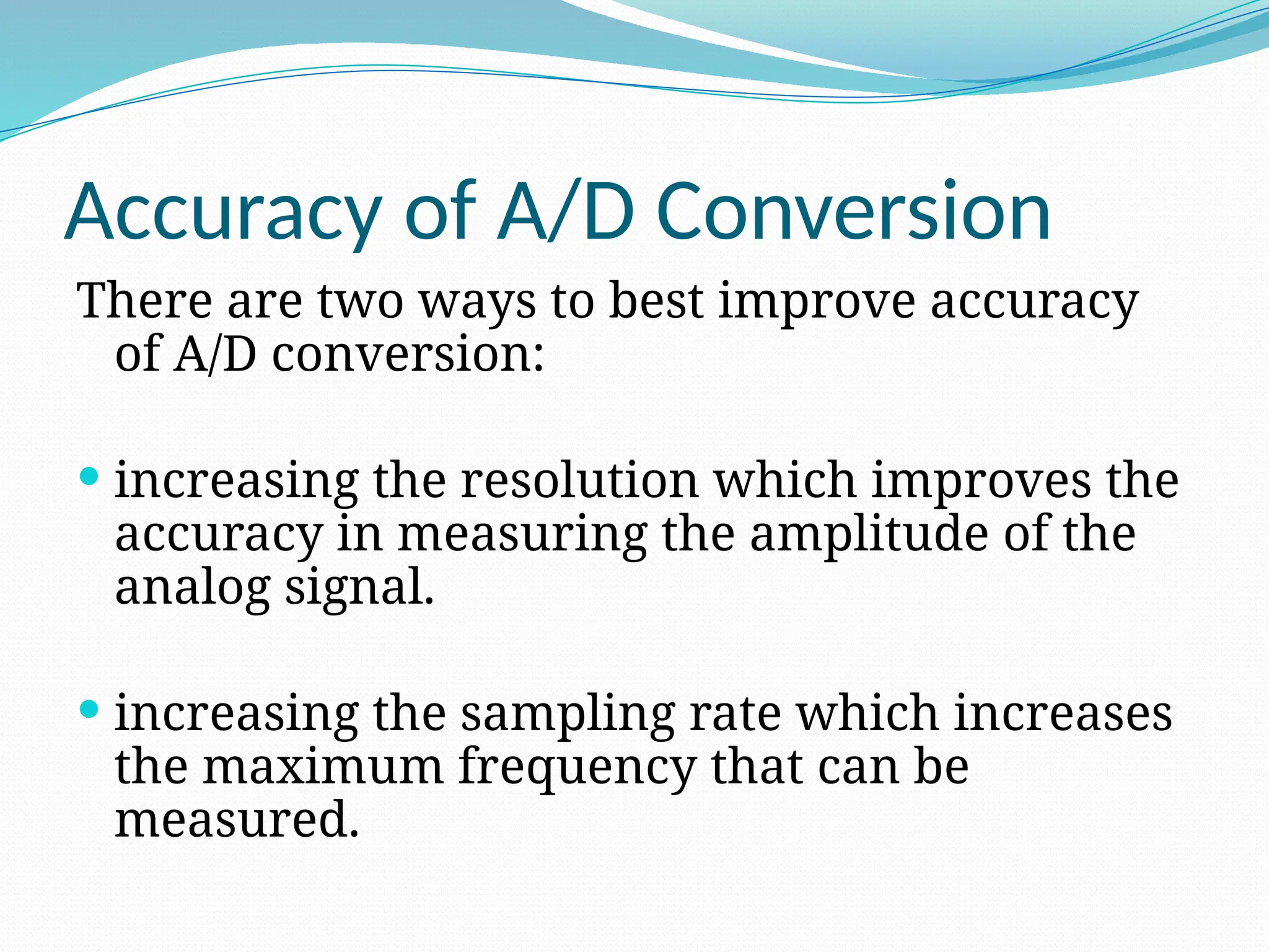
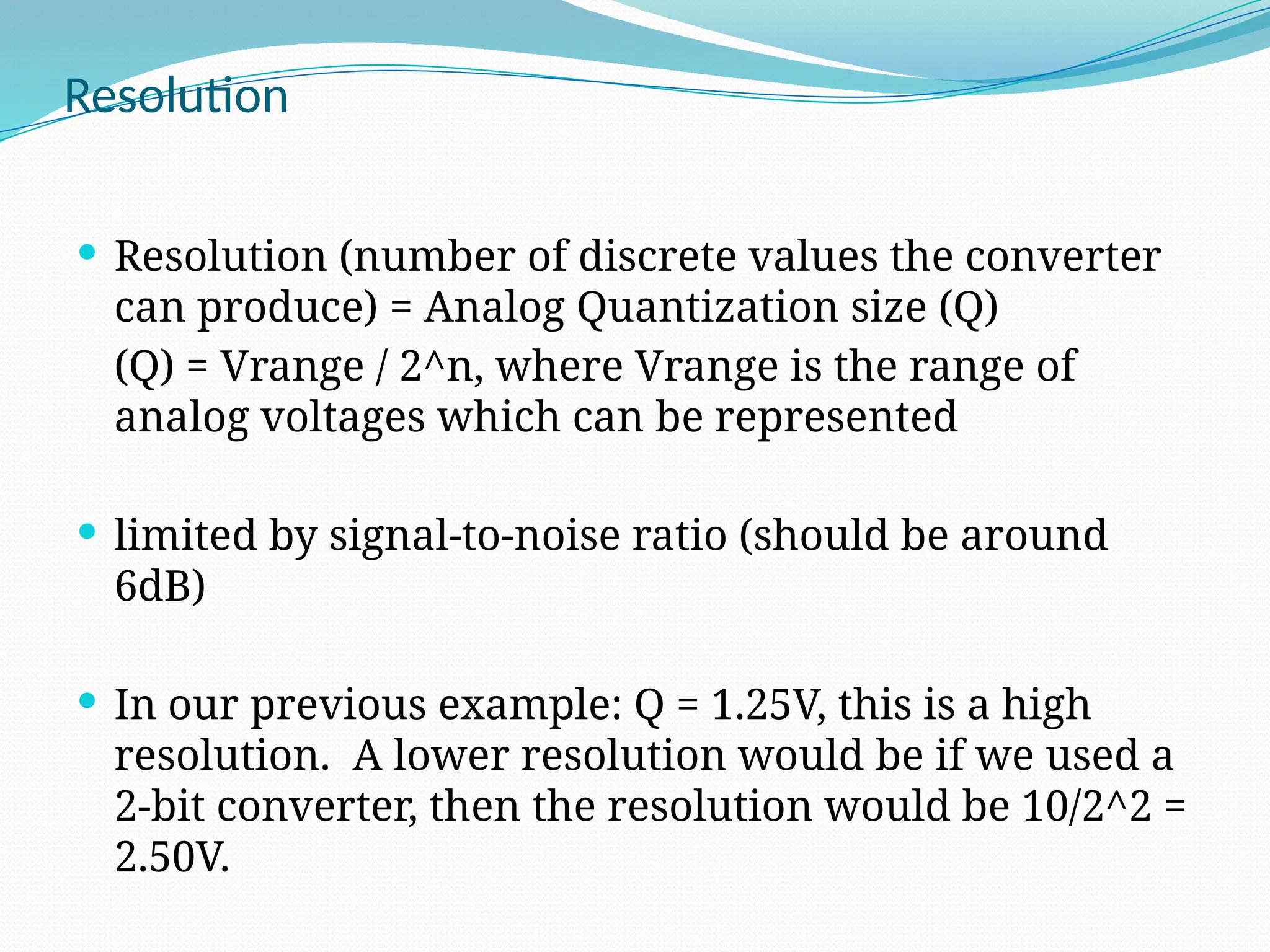
ADC 0804 Interfacing with
Microcontroller AT89C51
Prepared By:-
Akanksha Dixit
Asst. Prof.,EC Dept.
 ADC0804 is one of the most commonly used analog to digital
converter IC. In many applications it is required to convert the
output of the sensor, which is analogue in nature to a digital form.
The data in digital format can then be utilized for further processing
by the digital processors. Typical applications include sound
processing, temperature processing etc. This circuit demonstrates the
principle and operation of interfacing a simple ADC 0804 using 8051
microcontroller (AT89c51).
 ADC 0804.
 ADC0804 is an 8 bit successive approximation analogue to digital
converter from National semiconductors.
 The features of ADC0804 are :-
 Differential analogue voltage inputs,
 Built in clock generator,
 Reference voltage can be externally adjusted to convert smaller
analogue voltage span to 8 bit resolution etc.
ADC0804 is a single channel analog to digital convertor i.e.,
it can take only one analog signal. An ADC has n bit resolution
(binary form) where n can be 8,10,12,16 or even 24 bits. ADC
0804 has 8 bit resolution. The higher resolution ADC gives
smaller step size. Step size is smallest change that can be
measured by an ADC. For an ADC with resolution of 8 bits, the
step size is 19.53mV (5V/255).
The resolution of the converter indicates the number of
discrete values it can produce over the range of analog values
The pin out diagram of ADC0804 is shown in the figure below.
Pin Description:-
1.CS, Chip Select: This is an active low pin and used to activate the ADC0804.
2. RD, Read: This is an input pin and active low. After converting the analog data,
the ADC stores the result in an internal register. This pin is used to get the data
out of the ADC 0804 chip. When CS=0 & high to low pulse is given to this pin, the
digital output is shown on the pins D0-D7.
3.WR, Write: This is an input pin and active low. This is used to instruct the ADC to
start the conversion process. If CS=0 and WR makes a low to high transition, the
ADC starts the conversion process.
4. CLK IN, Clock IN: This is an input pin connected to an external clock source.
5.INTR, Interrupt: This is an active low output pin. This pin goes low when the
conversion is over.
6. Vin+ : Analog Input .
7. Vin- : Analog Input. Connected to ground.
8. AGND: Analog Ground.
9. Vref/2: This pin is used to set the reference voltage. If this is not connected the
default reference voltage is 5V. In some application it is required to reduce the
step size. This can be done by using this pin.
10. DGND: Digital Ground.
11-18. Output Data Bits (D7-D0).
19. CLKR: Clock Reset.
20. Vcc: Positive Supply
Analog and Digital Ground
 Analog ground is connected to the ground of the
analog Vin.
 Digital ground is connected to the ground of the
analog Vcc Pin.
 The voltage at Vref/2 (pin9) of ADC0804 can be
externally adjusted to convert smaller input
voltage spans to full 8 bit resolution. Vref/2 (pin9)
left open means input voltage span is 0-5V and
step size is 5/255=19.6V. Have a look at the table
below for different Vref/2 voltages and
corresponding analogue input voltage spans.
Vref/2 (pin9)
(volts)
Input voltage span
(volts)
Step size (mV)
Left open 0 – 5 5/255 = 19.6
2 0 – 4 4/255 = 15.69
1.5 0 – 3 3/255 = 11.76
1 0 – 2 2/255 = 7.84
0.5 0 – 1 1/255 = 3.92
 Make CS=0 and send a low to high pulse to WR pin to
start the conversion.
 Now keep checking the INTR pin. INTR will be 1 if
conversion is not finished and INTR will be 0 if
conversion is finished.
 If conversion is not finished (INTR=1) , poll until it is
finished.
 If conversion is finished (INTR=0), go to the next step.
 Make CS=0 and send a high to low pulse to RD pin to
read the data from the ADC.
Steps for converting the analogue input and reading the output from ADC0804.
Make CS=0 and send a low to high pulse to WR pin to
start the conversion.
Make CS=0 and send a low to high pulse to RD pin to
read the data from the ADC.
When CS=0 & low to high pulse is given to this pin, the digital
output is shown on the pins D0-D7.
Program.
ORG 00H
MOV P1,#11111111B // initiates P1 as the input port
MAIN: CLR P3.7 // makes CS=0
SETB P3.6 // makes RD high
CLR P3.5 // makes WR low
SETB P3.5 // low to high pulse to WR for starting conversion
WAIT: JB P3.4,WAIT // polls until INTR=0
CLR P3.7 // ensures CS=0
CLR P3.6 // high to low pulse to RD for reading the data from ADC
MOV A,P1 // moves the digital data to accumulator
CPL A // complements the digital data (*see the notes)
MOV P0,A // outputs the data to P0 for the LEDs
SJMP MAIN // jumps back to the MAIN program
END
Note
 The entire circuit can be powered from 5V DC.
 CS is set to low for RD and WR signals.
#include <REGX51.H>
sfr adc_port=0xa0;//ADC Port Port2
sbit rd=P1^0;//Read signal P1.0
sbit wr=P1^1;//Write signal P1.1
sbit cs=P1^2; //CHIP select signal P1.2
sbit intr=P1^3; //INTR signal P1.3
void conv();// Start of conversion function
void read();//Read ADC function
unsigned char adc_val;
void main ()
{
while(1)//forever loop
{
conv();//start convertion
read();//read ADC
P3=adc_val;//send read value to P3
}
}
void conv()
{
cs=0;//make cs low for activating ADC
wr=0;//make wr low ADC clear
wr=1;//make wr high ADC will starts conversion
cs=1; //make cs high
while(intr);//wait for INTR to go low
}
void read()
{
cs=0; //make cs low for activating ADC
rd=0; //make rd low
adc_val=adc_port;
rd=1; //make rd high
cs=1; //make cs high
}
How to interface ADC0804 using 8051
microcontroller (AT89C51)
Components:-
Microcontroller ADC0804 LED
AT890804
 The figure below shows the schematic for interfacing ADC0804
to 8051. The circuit initiates the ADC to convert a given
analogue input , then accepts the corresponding digital data
and displays it on the LED array connected at P3.
 For example, if the analogue input voltage Vin is 5V then all
LEDs will glow indicating 11111111 in binary which is the
equivalent of 255 in decimal.
 AT89s51 is the microcontroller used here.
 Data out pins (D0 to D7) of the ADC0804 are connected to the
port pins P2.0 to P2.7 respectively.
 In simple words P2 of the microcontroller is the input port and
P3 is the output port. Control signals for the ADC (RD, WR, CS
and INTR, ) are available at port pins P1.0 to P1.3 respectively.
 Resistor R1 and capacitor C1 are associated with the internal
clock circuitry of the ADC.
 Here sine pulse is applied as analog input voltage of amplitude
5 v to the ADC. When the input voltage from the preset is varied
the output of ADC varies which can be seen on the LCD. When
the preset is at minimum level, no LED glows and when the
preset is at maximum position all the LEDs starts glowing.
schematic for interfacing of ADC0804 to
AT89c51.
A/D converter
 Converts analog signals into binary words
Analog  Digital Conversion
2-Step Process:
 Quantizing - breaking down analog value is a set
of finite states
 Encoding - assigning a digital word or number to
each state and matching it to the input signal
Step 1: Quantizing
Example:
You have 0-10V
signals. Separate
them into a set of
discrete states with
1.25V increments.
(How did we get
1.25V? See next
slide…)
Output
States
Discrete Voltage
Ranges (V)
0 0.00-1.25
1 1.25-2.50
2 2.50-3.75
3 3.75-5.00
4 5.00-6.25
5 6.25-7.50
6 7.50-8.75
7 8.75-10.0
Quantizing
The number of possible states that the
converter can output is:
N=2n
where n is the number of bits in the AD
converter
Example: For a 3 bit A/D converter, N=23
=8.
Analog quantization size:
Q=(Vmax-Vmin)/N = (10V – 0V)/8 = 1.25V
Encoding
 Here we assign the
digital value
(binary number) to
each state for the
computer to read.
Output
States
Output Binary Equivalent
0 000
1 001
2 010
3 011
4 100
5 101
6 110
7 111
Accuracy of A/D Conversion
There are two ways to best improve accuracy
of A/D conversion:
 increasing the resolution which improves the
accuracy in measuring the amplitude of the
analog signal.
 increasing the sampling rate which increases
the maximum frequency that can be
measured.
Resolution
 Resolution (number of discrete values the converter
can produce) = Analog Quantization size (Q)
(Q) = Vrange / 2^n, where Vrange is the range of
analog voltages which can be represented
 limited by signal-to-noise ratio (should be around
6dB)
 In our previous example: Q = 1.25V, this is a high
resolution. A lower resolution would be if we used a
2-bit converter, then the resolution would be 10/2^2 =
2.50V.
THANKU

adcPresentation for microcontrolling process techniq

  • 1.
    ADC 0804 Interfacingwith Microcontroller AT89C51 Prepared By:- Akanksha Dixit Asst. Prof.,EC Dept.
  • 4.
     ADC0804 isone of the most commonly used analog to digital converter IC. In many applications it is required to convert the output of the sensor, which is analogue in nature to a digital form. The data in digital format can then be utilized for further processing by the digital processors. Typical applications include sound processing, temperature processing etc. This circuit demonstrates the principle and operation of interfacing a simple ADC 0804 using 8051 microcontroller (AT89c51).  ADC 0804.  ADC0804 is an 8 bit successive approximation analogue to digital converter from National semiconductors.  The features of ADC0804 are :-  Differential analogue voltage inputs,  Built in clock generator,  Reference voltage can be externally adjusted to convert smaller analogue voltage span to 8 bit resolution etc.
  • 5.
    ADC0804 is asingle channel analog to digital convertor i.e., it can take only one analog signal. An ADC has n bit resolution (binary form) where n can be 8,10,12,16 or even 24 bits. ADC 0804 has 8 bit resolution. The higher resolution ADC gives smaller step size. Step size is smallest change that can be measured by an ADC. For an ADC with resolution of 8 bits, the step size is 19.53mV (5V/255). The resolution of the converter indicates the number of discrete values it can produce over the range of analog values
  • 7.
    The pin outdiagram of ADC0804 is shown in the figure below.
  • 8.
    Pin Description:- 1.CS, ChipSelect: This is an active low pin and used to activate the ADC0804. 2. RD, Read: This is an input pin and active low. After converting the analog data, the ADC stores the result in an internal register. This pin is used to get the data out of the ADC 0804 chip. When CS=0 & high to low pulse is given to this pin, the digital output is shown on the pins D0-D7. 3.WR, Write: This is an input pin and active low. This is used to instruct the ADC to start the conversion process. If CS=0 and WR makes a low to high transition, the ADC starts the conversion process. 4. CLK IN, Clock IN: This is an input pin connected to an external clock source. 5.INTR, Interrupt: This is an active low output pin. This pin goes low when the conversion is over. 6. Vin+ : Analog Input . 7. Vin- : Analog Input. Connected to ground. 8. AGND: Analog Ground. 9. Vref/2: This pin is used to set the reference voltage. If this is not connected the default reference voltage is 5V. In some application it is required to reduce the step size. This can be done by using this pin. 10. DGND: Digital Ground. 11-18. Output Data Bits (D7-D0). 19. CLKR: Clock Reset. 20. Vcc: Positive Supply
  • 14.
    Analog and DigitalGround  Analog ground is connected to the ground of the analog Vin.  Digital ground is connected to the ground of the analog Vcc Pin.
  • 17.
     The voltageat Vref/2 (pin9) of ADC0804 can be externally adjusted to convert smaller input voltage spans to full 8 bit resolution. Vref/2 (pin9) left open means input voltage span is 0-5V and step size is 5/255=19.6V. Have a look at the table below for different Vref/2 voltages and corresponding analogue input voltage spans.
  • 18.
    Vref/2 (pin9) (volts) Input voltagespan (volts) Step size (mV) Left open 0 – 5 5/255 = 19.6 2 0 – 4 4/255 = 15.69 1.5 0 – 3 3/255 = 11.76 1 0 – 2 2/255 = 7.84 0.5 0 – 1 1/255 = 3.92
  • 19.
     Make CS=0and send a low to high pulse to WR pin to start the conversion.  Now keep checking the INTR pin. INTR will be 1 if conversion is not finished and INTR will be 0 if conversion is finished.  If conversion is not finished (INTR=1) , poll until it is finished.  If conversion is finished (INTR=0), go to the next step.  Make CS=0 and send a high to low pulse to RD pin to read the data from the ADC. Steps for converting the analogue input and reading the output from ADC0804.
  • 22.
    Make CS=0 andsend a low to high pulse to WR pin to start the conversion.
  • 24.
    Make CS=0 andsend a low to high pulse to RD pin to read the data from the ADC.
  • 25.
    When CS=0 &low to high pulse is given to this pin, the digital output is shown on the pins D0-D7.
  • 26.
    Program. ORG 00H MOV P1,#11111111B// initiates P1 as the input port MAIN: CLR P3.7 // makes CS=0 SETB P3.6 // makes RD high CLR P3.5 // makes WR low SETB P3.5 // low to high pulse to WR for starting conversion WAIT: JB P3.4,WAIT // polls until INTR=0 CLR P3.7 // ensures CS=0 CLR P3.6 // high to low pulse to RD for reading the data from ADC MOV A,P1 // moves the digital data to accumulator CPL A // complements the digital data (*see the notes) MOV P0,A // outputs the data to P0 for the LEDs SJMP MAIN // jumps back to the MAIN program END
  • 28.
    Note  The entirecircuit can be powered from 5V DC.  CS is set to low for RD and WR signals.
  • 29.
    #include <REGX51.H> sfr adc_port=0xa0;//ADCPort Port2 sbit rd=P1^0;//Read signal P1.0 sbit wr=P1^1;//Write signal P1.1 sbit cs=P1^2; //CHIP select signal P1.2 sbit intr=P1^3; //INTR signal P1.3 void conv();// Start of conversion function void read();//Read ADC function unsigned char adc_val; void main () { while(1)//forever loop { conv();//start convertion read();//read ADC P3=adc_val;//send read value to P3 } }
  • 30.
    void conv() { cs=0;//make cslow for activating ADC wr=0;//make wr low ADC clear wr=1;//make wr high ADC will starts conversion cs=1; //make cs high while(intr);//wait for INTR to go low } void read() { cs=0; //make cs low for activating ADC rd=0; //make rd low adc_val=adc_port; rd=1; //make rd high cs=1; //make cs high }
  • 31.
    How to interfaceADC0804 using 8051 microcontroller (AT89C51)
  • 32.
  • 33.
     The figurebelow shows the schematic for interfacing ADC0804 to 8051. The circuit initiates the ADC to convert a given analogue input , then accepts the corresponding digital data and displays it on the LED array connected at P3.  For example, if the analogue input voltage Vin is 5V then all LEDs will glow indicating 11111111 in binary which is the equivalent of 255 in decimal.  AT89s51 is the microcontroller used here.  Data out pins (D0 to D7) of the ADC0804 are connected to the port pins P2.0 to P2.7 respectively.  In simple words P2 of the microcontroller is the input port and P3 is the output port. Control signals for the ADC (RD, WR, CS and INTR, ) are available at port pins P1.0 to P1.3 respectively.
  • 34.
     Resistor R1and capacitor C1 are associated with the internal clock circuitry of the ADC.  Here sine pulse is applied as analog input voltage of amplitude 5 v to the ADC. When the input voltage from the preset is varied the output of ADC varies which can be seen on the LCD. When the preset is at minimum level, no LED glows and when the preset is at maximum position all the LEDs starts glowing.
  • 35.
    schematic for interfacingof ADC0804 to AT89c51.
  • 45.
    A/D converter  Convertsanalog signals into binary words
  • 46.
    Analog  DigitalConversion 2-Step Process:  Quantizing - breaking down analog value is a set of finite states  Encoding - assigning a digital word or number to each state and matching it to the input signal
  • 47.
    Step 1: Quantizing Example: Youhave 0-10V signals. Separate them into a set of discrete states with 1.25V increments. (How did we get 1.25V? See next slide…) Output States Discrete Voltage Ranges (V) 0 0.00-1.25 1 1.25-2.50 2 2.50-3.75 3 3.75-5.00 4 5.00-6.25 5 6.25-7.50 6 7.50-8.75 7 8.75-10.0
  • 48.
    Quantizing The number ofpossible states that the converter can output is: N=2n where n is the number of bits in the AD converter Example: For a 3 bit A/D converter, N=23 =8. Analog quantization size: Q=(Vmax-Vmin)/N = (10V – 0V)/8 = 1.25V
  • 49.
    Encoding  Here weassign the digital value (binary number) to each state for the computer to read. Output States Output Binary Equivalent 0 000 1 001 2 010 3 011 4 100 5 101 6 110 7 111
  • 50.
    Accuracy of A/DConversion There are two ways to best improve accuracy of A/D conversion:  increasing the resolution which improves the accuracy in measuring the amplitude of the analog signal.  increasing the sampling rate which increases the maximum frequency that can be measured.
  • 51.
    Resolution  Resolution (numberof discrete values the converter can produce) = Analog Quantization size (Q) (Q) = Vrange / 2^n, where Vrange is the range of analog voltages which can be represented  limited by signal-to-noise ratio (should be around 6dB)  In our previous example: Q = 1.25V, this is a high resolution. A lower resolution would be if we used a 2-bit converter, then the resolution would be 10/2^2 = 2.50V.
  • 52.